I. INTRODUCTION
Many current microsystems require the integration of a number of small components that are made in potentially incompatible fabrication technologies. Furthermore, the recent trend in building systems with unconventional form factors and on unconventional materials such as flexible plastics necessitates the development of methods that can place and interconnect components—of ever decreasing size—onto such substrates.
Currently, robotic assembly is dominantly used for integration of millimeter-scale components down to a few hundred micrometers.Reference Morris, Stauth and Parviz1 Robots perform the assembly task for various components and platforms, with much flexibility in choosing the component geometry or the template material. Robotic assembly has high yield and accuracy in placing the components at the designated sites, but the assembly speed and cost become restricting factors as the component size decreases or the area of assembly increases. Hence, new methods are required to integrate separately fabricated parts and components onto a template at smaller scales (less than a few hundred micrometers).
Self-assembly, the spontaneous formation of structures by properly designed components is a potent candidate to meet the future integration needs. It has been shown that self-assembly is a promising technique for component integration on a template or in the form of three-dimensional structures at micron and sub-micron scales.Reference Mastrangeli, Abbasi, Varel, Hoof, Celis and Bohringer2, Reference Whitesides and Grzybowski3 Self-assembly is a fast and cost-effective method due to its parallel nature and the capability to integrate a large number of components over desired surfaces.Reference Morris, Stauth and Parviz1, Reference Mastrangeli, Abbasi, Varel, Hoof, Celis and Bohringer2, Reference Whitesides and Grzybowski3 One essential requirement for all packaging methods (including self-assembly) is the ability to integrate heterogeneous parts and components to the proper locations. For the self-assembly approach to be effective for heterogeneous integration, means must be devised to control and program the process to be able to guide each component to assemble onto the proper location.
Self-assembly has been programmed in the nanoscale using techniques such as DNA hybridization and peptide surface binding.Reference Keren, Berman, Buchstab, Sivan and Braun5, Reference Mirkin6 Using biomolecular interactions as the driving force for self-assembly provides inherent programmability due to the specificity of these reactions and the capability to suppress them. Strong biotin-avidin binding was used to self-assemble nanorods head to tail or side by side.Reference Salant, Sadovsky and Banin7–Reference Chen, Guo, Ravi and Searson9 Hybridization of ss-DNA attached to nano-objects was used to self-assemble specific components such as carbon nanotubes, nanorods, and silicon islands on templates.Reference Lee, McNally, Guo, Pingle, Bergstrom and Bashir10–Reference Morrow, Li, Kim, Mayer and Keating13
Microscale self-assembly has been programmed using various techniques such as controlling surface hydrophobicity, controlling solder alloy activation, and applying dielectrophoresis forces. Xiong et al.Reference Xiong, Hanein, Fang, Wang, Wang, Schwartz and Böhringer14 used the capillary forces between hydrophobic components and pads on the template as the driving force for self-assembly. They were able to assemble two types of components by changing the hydrophobicity of the pads using electrochemical desorption of a self-assembled monolayer. Liu et al.Reference Liu, Lau and Yang15 used the capillary force between molten alloys on a template and metal pads on the components to drive the self-assembly. They self-assembled two types of components by using alloys with two different melting points. The proper site on the template was activated for each type of component by step heating the fluid environment. Chung et al.Reference Chung, Zheng, Hatch and Jacobs16 used microheaters to locally melt solder alloy and assemble different color light-emitting diodes (LEDs) onto designated locations on a flexible template. SharmaReference Sharma17 used heater elements to form a gel around designated sites on the template and block the self-assembly around those sites. Furthermore, single particle/cell assembly with programmable patterns on photoconductive surfaces has been shown, using an optical image-driven dielectrophoresis technique.Reference Chiou, Ohta and Wu18 Dielectrophoresis force, which requires active participation of the template, was used to manipulate various components such as cells, LEDs, nanorods, and silicon parts to assemble each object in specific locations on a template.Reference Subramanian, Vikramaditya, Nelson, Bell and Dong19–Reference Papadakis, Gu and Gracias22
Many of the programmable self-assembly methods that are discussed here have been able to achieve high yields. However, most of these methods require active participation of the template, which would exert limitations on template material or add to the complexity of the template structure. The programming methods that are based on the surface chemistry of materials (e.g., molten alloys or molecular monolayers) are not extendable to a large number of component types. An ideal self-assembly programming method should be able to integrate a large variety of heterogeneous components in a massively parallel fashion by placing minimal restrictions on template and component materials and structures.
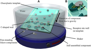
Our group has previously shown a number of applications for micron-scale self-assembly.Reference Morris and Parviz23–Reference Stauth and Parviz25 In our self-assembly method, functional microcomponents are independently microfabricated and released from a carrier wafer to form a collection of free-standing parts suspended within a fluid. These microcomponents are subsequently passed over a template, containing receptor sites that provide locations for the microcomponents to be assembled and complete the system. Figure 1 shows the overview of the self-assembly process. The self-assembly template is held at an angle inside the fluid medium. Gravity exerts a downward force on the components to slide on the template until they reach a receptor site well. In recent designs, we have fabricated a C-shaped trap by each receptor site on the template [Fig. 1(b)] to increase the probability of components being trapped in the receptor sites. Self-assembly occurs as the component hits the C-shaped trap, and falls inside the receptor site well.
Schematic of the self-assembly process. (a) Microcomponents are introduced over the template submerged in liquid. External agitation and gravity help the microcomponents to move toward the bottom of the template and experience random collisions. C-shaped walls trap the components that are passing over a receptor site. (b) Enlarged view of one component (circular 1-notch) entering a receptor site on the template. Self-assembly happens when the component hits the C-shaped wall and falls inside the receptor site well.

We have shown that shape recognition between the microcomponents and complementary shaped receptor site wells on a common template can be used to program the self-assembly process to some extent.Reference Stauth and Parviz25 We were able to self-assemble various functional microcomponents on templates using this method.Reference Saeedi, Kim and Parviz24, Reference Stauth and Parviz25 However, controlling the self-assembly process on the basis of shape recognition was limited due to geometric constraints that were placed on component and receptor site shapes. Furthermore, the method was incapable of assembling two component types that had identical geometries but different functionalities.
Here, we present a more versatile method to optically control the microscale self-assembly process of multibatch components that is compatible with unconventional substrates such as plastic and glass. This method builds on our previous experiments with micron-scale self-assembly and uses widely available optical lithography tools to control the assembly process with light.
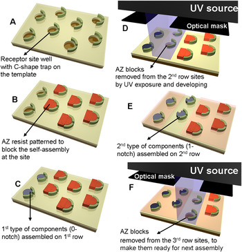
The method to optically control the self-assembly process is schematically shown in Fig. 2. The process starts with preparing a template, complete with electrical connections and receptor sites, and a series of microcomponents. The receptor sites on the template are initially blocked with a photosensitive polymer structure. A particular receptor site may be made available by selectively exposing the light-sensitive blocking polymer in the site to light and its subsequent removal. Once the site becomes available, the method depicted in Fig. 1 can be used to place a microcomponent in its location. The newly assembled microcomponent may be fixed in place with an alloy connection or by coating with another layer of photosensitive polymer. The previous steps may be repeated a number of times to assemble various microcomponents onto different locations on the template.Reference Saeedi, Etzkorn, Deraghi and Parviz26 The method can handle a large number of microcomponents in parallel and accurately place them. The method outlined here enables an arbitrary location to be chosen for the self-assembly of a given component. Hence, using the same template and component set, but a different exposure sequence or pattern, a new system can be created on the substrate. A major advantage of the method is its flexibility. When used in conjunction with a maskless photolithography system, the placement of microcomponents could be easily reprogrammed. Hence, a standard template and a standard set of microcomponents could be used to make a large number of different microsystems.
Overview of the steps for optically controlling the self-assembly process at specific locations on a template. AZ4620 photoresist (AZ) was patterned onto the template to cover the receptor sites and block the self-assembly of components. UV exposure through a mask and development were used to remove the AZ blocks from the designated areas before each step of the self-assembly process. (a) Fabricated template with receptor site wells and C-shaped traps. (b) AZ resist was spin-coated and patterned to cover all the receptor sites, except the sites on the first row. (c) First type of microcomponents (circular 0-notch) was allowed to self-assemble in the available sites. (d) Thin layer of AZ resist was spin-coated on the whole template to fix the assembled components in place. UV exposure through a mask and development remove the AZ blocks from the second row sites on the template. (e) Second type of components (circular 1-notch) was allowed to self-assemble. (f) Similar to part (d), the AZ blocks were removed from the third row to make it ready for assembly of the third type of components. By repeating these steps, one can assemble many types of microcomponents on a common template.

In the following sections, we demonstrate the use of the method to sequentially self-assemble four different mock silicon microcomponent types at specific locations on a template. We describe how the microcomponents and the templates were prepared and how the self-assembly experiments were carried out. We used this system for studying the yield of the optically controllable self-assembly process. We conclude by discussing the self-assembly of two similarly shaped functional microcomponents—red light-emitting diodes and silicon resistors—and a brief section of concluding remarks.
II. MICROCOMPONENTS AND TEMPLATE FABRICATION
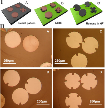
Four different circular silicon microcomponents (having 0, 1, 2, or 3 notches) were fabricated to demonstrate the optically controllable self-assembly process. The fabrication process for the microcomponents is shown in Fig. 3(I). Microcomponents were fabricated on a silicon-on-insulator (SOI) wafer. The boron-doped SOI wafer (~1 Ω.cm resistivity) had a 20-μm device layer on top of a 2-μm oxide layer. The SOI wafer was cleaned [piranha, acetone, and isopropanol (IPA)] and a 6.4-μm layer of AZ4620 positive photoresist was spin-coated and patterned to define the shape of the circular components. A deep reactive ion etcher (DRIE) was then used to etch the silicon down to the buried silicon dioxide layer in the wafer using the AZ resist layer as the mask. The microcomponents were then released by wet etching the silicon dioxide sacrificial layer in HF. The circular silicon components were 20 μm thick and 320 μm in diameter. Components were then collected and cleaned in acetone (to remove the AZ photoresist) and HCl. Finally, the components were stored in deionized (DI) water to be later used for the self-assembly process. Figure 3(II) shows optical microscope images of released microcomponents on a glass slide.
Si microcomponent fabrication. (I) Process flow for fabrication of four types of circular components on a SOI wafer. (II) Microscope image of representative released microcomponents on a glass slide.

We also fabricated two types of functional microcomponents (red-emitting LEDs and silicon resistors) with the same geometries and metal contact configuration to show the use of the described method for self-assembly of seemingly similar components on a template. The AlGaAs LEDs fabrication process and properties are discussed in Ref. 24. The LEDs emit bright red light with a peak wavelength of 689 nm. Silicon resistors were fabricated with a process flow very similar to silicon components shown in Fig. 3(I), with the only addition being metal pads on the components. This was accomplished by a metal deposition and lift-off step prior to the DRIE shape definition. The metal pads for resistors (Cr/Au, 20 nm/250 nm) were deposited with the same shape and size as those used for LEDs.Reference Saeedi, Kim and Parviz24 Released circular resistors had a 320 μm diameter (same as LEDs) and were 20 μm thick. The measured resistance for each silicon component was 424 Ω.
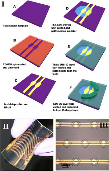
Templates for self-assembly were fabricated on both plastic and glass. We used 175-μm-thick flexible polyethylene terephthalate (PET) sheets for plastic template fabrication. The fabrication process flow is shown in Fig. 4(I). A 6.4-μm layer of positive AZ4620 photoresist was first spin-coated and photolithographically patterned on the plastic/glass template surface to define the shape of the metal contacts. A 217-nm-thick metal (Cr/Ni/Au, 27 nm/90 nm/100 nm) layer was then deposited on the template using electron beam evaporation. Metal was then removed from nonexposed areas on the template by lift-off in acetone. A thin layer (1.4 μm) of negative SU8 photoresist was spin-coated and patterned inside the receptor site wells on the template to isolate each metal contact. The only exposed areas in receptor site wells were two oval-shaped metal pads that later would be connected to the metal pads on the microcomponents. Receptor site wells and C-shaped traps were then patterned using a thick layer of SU8 negative resist. Each binding site on the template consisted of a circular well (16.1 μm deep, 350 μm diameter) under a C-shaped trap (17.3 μm tall). Finally, all the binding sites were “blocked” by photolithographically patterning a thick layer of AZ4620 photoresist (23.2 μm). A completed flexible plastic template containing an array of 640 traps and optical microscope image of a few representative receptor sites (with no blocking resist) are shown in Figs. 4(II) and 4(III), respectively.
Template fabrication. (I) (a–e) Process flow for plastic or glass template fabrication. (II) A complete flexible plastic template. (III) Microscope image of a few circular receptor site wells with C-shaped traps on a plastic template.

Due to the relatively low glass transition temperature of PET (69 °C), some of the microfabrication steps were altered to ensure the integrity of the plastic template, such as baking temperature, baking duration, and metal deposition rates. Photoresist baking was performed below 65 °C, and metal deposition rates were kept below 3 Å/sec. The plastic and the glass templates had similar geometries and a top surface covered by SU8. In our experiments, both substrate types demonstrated the same self-assembly yield.
III. SELF-ASSEMBLY PROCESS AND RESULTS
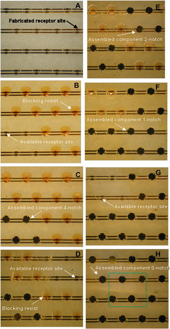
To perform the self-assembly process, the template was kept at a ~30° angle and submerged in water while microcomponents were introduced and flowed over its surface. Gravity, fluid flow forces, and external agitation helped the microcomponents move down the sloped template until they were trapped in a receptor site well [Fig. 1(b)]. Starting with the template with fabricated receptor site wells and traps [Fig. 5(a)], all the receptor sites except the ones that were designated for assembly of 4-notch components were blocked by AZ resist during the first assembly step [Fig. 5(b)]. During the first self-assembly step, 4-notch components were populated in proper receptor site wells with a high yield [Fig. 5(c)]. A thin layer of AZ1512 resist (1.8 μm) was then spin-coated over the template to keep the assembled components in place and also to protect the remaining blocking resist from etching and degrading during subsequent developing steps.
Optical microscope images of a sequence of events during the self-assembly process of four different microcomponent types. (a) Fabricated receptor site wells and C-shaped traps on a plastic template prior to self-assembly. (b) AZ resist was patterned on the template to block all the receptor sites, except the four receptor sites located on the bottom left. (c) The first type of components (circular 4-notch) was assembled within the 2 × 2 parallelogram pattern of available receptor sites. (d) A thin layer of AZ was coated on the whole template to fix the assembled microcomponents. The blocking resist was then removed from the four top right receptor sites designated for the second type of microcomponents. (e) The second type of components (circular 2-notch) was assembled in available receptor sites. (f) The third type of components (circular 1-notch) was assembled in the bottom left corner of the image in a similar fashion. (g) AZ resist was removed from the remaining four receptor sites on the top left. (h) Final type of components (circular 0-notch) was self-assembled. Zoomed-in image of dashed area is shown below in Fig. 6(a).

Before performing the second self-assembly step, the template was exposed to ultraviolet (UV) through a mask for 70 s and then developed for 7 min to remove the blocking resist from the receptor sites designated for the second type of components (2- notch) as shown in Fig. 5(d). The UV source used in all of our experiments had the intensity of 25 mW/cm2 at 405-nm wavelength. Next, the second self-assembly step was performed to integrate 2-notch components on the template [Fig. 5(e)]. We repeated these steps two more times to self-assemble all four component types as shown in Fig. 5(h).
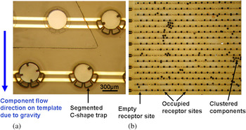
A magnified image of the dashed area in Fig. 5(h) containing all four assembled microcomponent types is shown in Fig. 6(a). The segmented structure for the C-shaped traps facilitated better movement of fluid and components around the receptor sites on the template. A section of the completed array containing 640 receptor sites is shown in Fig. 6(b).Reference Saeedi, Etzkorn, Deraghi and Parviz26
(a) Magnified view of dashed area shown in Fig. 5(h) showing all four microcomponent types assembled in the proper locations. (b) Zoomed-out view of a section of the completed template with 640 receptor sites after self-assembly of all four component types. The figure highlights the high occupancy rate and some of the failure mechanisms of the method.

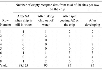
We have performed a large number of successful self-assembly experiments to quantify the yield of the process. Typical yield results for one component type are shown in Table I. The numbers displayed in Table I are for 1-notch microcomponents self-assembly in fluid medium, followed by removing the template from water, and removing the blocking resist to make the chip ready for the next microcomponent type self-assembly step. Yield results for all four component types showed very similar trends within 3% of the numbers reported in Table I. We obtained a high initial yield of accurate component placement on the template (~98% yield) and this was achieved after ~10 min of fluid flow containing three times the number of microcomponents compared to the number of available receptor sites. The yield was reduced to 85% later mainly during the photoresist coating step performed to fix the components in place. A commonly observed defect was the adhesion of the microcomponents onto unwanted locations on the template due to surface forces. Surface forces became much stronger at small scales, due to the large surface-area-to-volume ratio of the component, increasing the chance of microcomponent adhering to each other or the template erroneously. Strong fluid flow helped remove most of the incorrectly bound microcomponents, but some clusters still remained as shown in Fig. 6(b). The agitation from the external shaker further aided the removal of microcomponents stuck to previously assembled components or undesired locations on the surface allowing the dislodged components to flow down the template to available receptor site wells.
Typical yield table for all the steps required to assemble one type of component.

We stopped the self-assembly (SA) after ~10 min, which resulted in an initial 98% yield for filling the receptor sites with microcomponents. The assembly yield reduced to 85% after manual wafer handling and spin coating the AZ fixing layer. This reduction in yield can be avoided by using an automated system.
The yield numbers reported in Table I are based on placement, without any chemical bonding to the template. We have already shown that by using a molten alloy on the template, the self-assembled components will form a mechanical and electrical connection to the template, which is essential for making a functional system. The detailed yield numbers for the electrical connection from molten alloys, and parameters affecting the yield, are explained in previous publications. Reference Morris and Parviz23–Reference Stauth and Parviz25
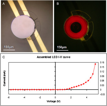
Next, we demonstrated self-assembly of red LEDs and resistors with electrical connections. A small volume of alloy was deposited on exposed oval-shaped metal pads inside each well by dipping the template in a molten alloy bath at 85 °C, immediately before performing the self-assembly process. The molten alloy in the receptor site wells would then wet the metal pads on the microcomponents to form electrical and mechanical bonds. For these experiments we used lead-free solder (elemental composition: In 51%, Bi 32.5%, Sn 16.5%; acquired from Indium Corporation, IL, USA) that had a melting point of 60 °C. Self-assembly was performed in acidic water (pH ~3) by adding hydrogen chloride to DI water. The self-assembly fluid medium temperature was increased to 85 °C to melt the alloy and to form electrical connections between template and the microcomponents. Figure 7 shows microscope images of a functional self-assembled LED with electrical connection on the template. The IV curve of the same LED self-assembled on a plastic template was measured and shown in Fig. 7(c).
Self-assembled circular red LED on the plastic template, with C-shaped traps. (a) Microscope image of an assembled LED. (b) Same LED connected to 5.5 V and emitting bright red light. (c) Measured IV curve of the same LED on the plastic template.

Silicon resistors were also self-assembled on plastic templates of the same design. The template was designed such that all assembled resistors in the same row were connected in parallel [Fig. 4(III)]. We measured a resistance of 99 Ω through one row on the plastic template that had five resistors successfully self-assembled. This number indicates a total contact resistance between microcomponents and template of ~71 Ω (or half this value on average for each connection).
While the orientation of the components was not an issue for mock silicon components, the correct orientation of the self-assembled LEDs and resistors was crucial to be able to make functional devices, because these components had metal contacts on only one side of them. The components trapped in receptor site wells with correct orientation were able to form a permanent mechanical bond to the template by molten alloy. On the other hand, for components trapped in receptor sites with incorrect orientation, the fluid flow may be reversed to remove the component and increase the yield. The yield of electrical connection and parameters affecting the molten alloy is discussed in more detail in previous publications..Reference Morris and Parviz23–Reference Stauth and Parviz25
IV. CONCLUSION
Self-assembly is a promising candidate to meet the demands to integrate a large number of microscale components expediently and cost effectively on various templates. Methods to program the self-assembly process are needed to make the approach flexible and applicable to diverse applications with minimum change to the microcomponent or the template structures. We have demonstrated a method based on light activation of the assembly sites that can readily achieve these goals. An important aspect of the method is that it can be deployed in conjunction with conventional lithography systems.
We detailed how four different silicon microcomponent types can be produced and controllably assembled with yields reaching 85%. The yield can be significantly improved by reducing the manual handling, using automation for motion and fluid flow, and taking advantage of maskless lithography.
We also showed that the method can be used to self-assemble two microcomponents that have the same face geometry but different functionalities. The integration of red LEDs and silicon resistors on plastic verify the versatility of the method for incorporation of high-performance crystalline semiconductor components on unconventional substrates.
ACKNOWLEDGMENTS
We gratefully acknowledge financial support from the National Institute of Health (NHGRI) through Microscale Life Sciences Center at the University of Washington. We also acknowledge support from the University of Washington (UW) Technology Gap Innovation Fund and Washington Research Foundation. We thank the staff of the Microfabrication Laboratory at the Washington Technology Center for providing crucial help with cleanroom microfabrication processes.