Introduction
Over the past few years, a breakthrough has occurred in the photovoltaic (PV) field by using inorganic–organic hybrid layers called perovskites as the light harvester in solar cells. The inorganic layers consist of sheets of corner-sharing metal halide octahedra. The cation (M) is generally a divalent metal that satisfies charge balancing and adopts octahedral anion coordination. The inorganic layers are usually called perovskite sheets, because they are derived from the three-dimensional AMX3 perovskite structure (where A = organic molecule, X = halide, and M = metal). The organic component consists of a bilayer or a monolayer of organic cations.
The inorganic–organic arrangement is self-assembled as alternate layers by a simple, low-cost procedure. These inorganic–organic hybrids promise several benefits that are not provided by the separate constituents, Reference Kojima, Ikegami, Teshima and Miyasaka1–Reference Mitzi, Field, Schlesinger and Laibowitz3 including mechanical rigidity, chemical stability and conductivity of the inorganic sheets, adjustable inter-sheet coupling by the organic part, and large absorption coefficient of the entire hybrid structure. These properties show good potential for the use of these materials as light harvesters in heterojunction solar cells. Due to intensive work on the perovskite structure, the solar-cell structure, and the deposition techniques (one-step/two-step deposition and co-evaporation of perovskite films) of the different active layers, Reference Lee, Teuscher, Miyasaka, Murakami and Snaith4–Reference Chen, Pan, Liu, Cai, Kou, Huo, Fang and Dai18 the efficiency currently achieved is approximately 20.1%. 19
Exceptional properties of the perovskite are the high mobility of charges (mobility refers to how the charge moves through a semiconductor under an electric field) and long diffusion lengths of electrons and holes (diffusion length is the distance a carrier travels between generation and recombination), which are some of the reasons for the high solar-cell efficiency achieved. Reference Stranks, Eperon, Grancini, Menelaou, Alcocer, Leijtens, Herz, Petrozza and Snaith20,Reference Xing, Mathews, Sun, Lim, Lam, Grätzel, Mhaisalkar and Sum21 However, prior to the discovery of these significant properties, pioneering work Reference Etgar, Gao, Xue, Peng, Chandiran, Liu, Nazeeruddin and Graetzel13 was published that reported on the use of HTM-free perovskite heterojunction solar cells. The authors found that a lead halide perovskite can transport holes, in addition to its functionality as a light harvester. Avoiding the use of a HTM in the solar cell has several advantages, including reducing the cost, avoiding oxidation, simplifying fabrication of the solar cell, and providing consistent results. However, it must be noted that when eliminating an important layer in the solar-cell structure (such as the HTM), the PV performance decreased. Nevertheless, recently, perovskite solar cells without a hole conductor achieved a power-conversion efficiency (PCE) of 10.85%. Reference Laben and Etgar22–Reference Aharon, Gamliel, Cohen and Etgar26 In addition, a fully printable mesoscopic perovskite solar cell using a porous carbon film reportedly achieved 12.8% efficiency. Reference Mei, Li, Liu, Ku, Liu, Rong, Xu, Hu, Chen, Yang, Grätzel and Han27
This article presents an overview on perovskite solar-cell structures without a HTM. The following topics are discussed: the mechanism in HTM-free solar cells; the possibility of gaining high voltage even without the HTM in these perovskite-based solar cells; different perovskites that can function simultaneously as a light harvester and a hole conductor; different contacts and their influence on PV performance; and recent demonstration of a panchromatic response combining the perovskite with near-infrared (NIR) quantum dots (QDs) in HTM-free structures.
HTM-free perovskite solar-cell structure
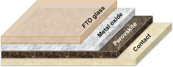
The solar-cell structure of a hole-conductor-free perovskite device is shown in Figure 1 . It consists of a conductive glass coated with a metal oxide (flat or porous) followed by organometal perovskite deposition on top of the metal oxide. A metal contact is then deposited.
The hole-conductor-free perovskite solar-cell structure. Note: FTO, fluorine-doped tin oxide.

Depletion region in HTM-free perovskite solar cell
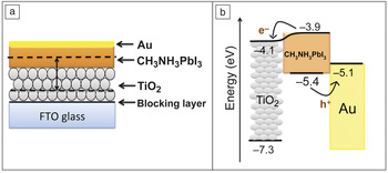
Due to the unique solar-cell structure, questions regarding the mechanism of the solar cell can be raised. Avoiding the HTM affects PV performance, although it also defines more clearly the interfaces at the solar-cell layers—in particular, the metal oxide/perovskite interface, which has a major influence on the PV performance of this solar cell. Capacitance–voltage measurements were carried out in order to observe the doping density and the depletion region width at this interface. Reference Aharon, Gamliel, Cohen and Etgar26 Figure 2 a shows the depleted HTM-free CH3NH3PbI3/TiO2 heterojunction solar cell where the depletion region width is indicated by the arrow in the figure. The energy-level diagram is shown in Figure 2b. Due to charge transfer from the electron accepting contact to the perovskite CH3NH3PbI3 film, a depletion layer might form. On illumination, the perovskite absorbs the light; as a result, electrons are transferred to the TiO2, and holes are transported to the gold contact.
(a) The structure of the hole-conductor-free TiO2/CH3NH3PbI3 perovskite-based solar cells. The vertical arrow indicates the depletion region observed at the TiO2/CH3NH3PbI3 junction. (b) Energy-level diagram of the discussed solar cell, which shows the charge separation process. The position of the energy levels is taken from Reference 13. Reprinted with permission from Reference 26. © 2014 Royal Society of Chemistry. Note: FTO, fluorine-doped tin oxide.

A correlation was found between the depletion layer width at the TiO2/CH3NH3PbI3 junction and the PCE. In the case of the highest efficiency, the total depletion width is at a maximum, suggesting that the depletion region assists in the charge separation and suppresses the back reaction, and, consequently, contributes to the increase in the PCE of the cells. A power conversion efficiency of 10.85% was achieved for these hole-conductor free perovskite solar cells. Reference Aharon, Gamliel, Cohen and Etgar26
High voltage in HTM-free perovskite solar cell
One of the attractive properties of organometal halide perovskites is their ability to gain high open-circuit voltage (V oc) with a high ratio of qV oc/E g (where q is the elementary charge of an electron, and E g is bandgap energy). A V oc of 1.3 V was achieved when using N,N′-dialkylperylenediimide as the HTM, with CH3NH3PbBr3 as the sensitizer/absorber. Reference Edri, Kirmayer, Cahen and Hodes28 Recently, a V oc of 1.5 V was reported when using CH3NH3PbBr3−x Cl x with 4,4′-bis(N-carbazolyl)-1,1′-biphenyl as the hole conductor. Reference Edri, Kirmayer, Kulbak, Hodes and Cahen29 High efficiency (6.7%) and high voltage (1.4 V) were demonstrated with a HTM based on tri-arylamine polymer derivatives containing fluorene and indenofluorene. Reference Ryu, Noh, Jeon, Kim, Yang, Seo and Seok30 Edri et al. Reference Edri, Kirmayer, Cahen and Hodes28,Reference Edri, Kirmayer, Kulbak, Hodes and Cahen29 and Ryu et al. Reference Ryu, Noh, Jeon, Kim, Yang, Seo and Seok30 reported using HTM to tune the voltage of the cell and gain high V oc.
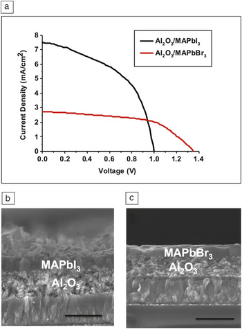
However, other recent reports Reference Noh, Im, Heo, Mandal and Seok12,Reference Etgar, Gao, Xue, Peng, Chandiran, Liu, Nazeeruddin and Graetzel13 show that the voltage in the perovskite solar cells is not determined simply by the difference between the Fermi levels of TiO2 and the HTM. A question can be raised regarding the possibility of gaining high V oc even without a HTM. Indeed, a recent study reported high V oc in HTM-free perovskite solar cells. Reference Dymshits, Rotem and Etgar31 In this work, an open-circuit voltage of 1.35 V was achieved in Al2O3/CH3NH3PbBr3/Au perovskite solar cells with a HTM-free configuration.
Figure 3 a shows the current density–voltage curves of the configuration of the two cells, Al2O3/CH3NH3PbBr3/Au and Al2O3/CH3NH3PbI3/Au, where V oc of 1.35 V and 1 V, respectively, were demonstrated. Reference Dymshits, Rotem and Etgar31 High-resolution scanning electron microscopy (HRSEM) cross-sections of both HTM-free configurations are shown in Figure 3b–c. Surface photovoltage measurements under light show a twofold difference in the contact potential difference between CH3NH3PbBr3 and CH3NH3PbI3, resulting in smaller surface potential for the Al2O3/CH3NH3PbBr3/Au cells.
(a) Current density–voltage curves of Al2O3/CH3NH3PbBr3/Au and Al2O3/CH3NH3PbI3/Au hole-transport material (HTM)-free solar cells show the high open-circuit voltage of the HTM free solar cells. High-resolution scanning electron microscopy image of the cross-section of (b) Al2O3/CH3NH3PbI3 and (c) Al2O3/CH3NH3PbBr3. Reprinted with permission from Reference 31. © 2014 Royal Society of Chemistry. Note: MA, methylammonium. The scale bar is 500 nm.

In addition, incident-modulated photovoltage spectroscopy (an electrochemical method to measure the recombination lifetime of a material at different light intensities) shows a longer recombination lifetime for the Al2O3/CH3NH3PbBr3 cells compared to the other cell configurations, further supporting the high open-circuit voltage. Reference Dymshits, Rotem and Etgar31 The possibility of gaining high open-circuit voltage even without a HTM in perovskite solar cells shows that the perovskite/metal oxide interface has a major effect on the open-circuit voltage in perovskite-based solar cells.
Panchromatic response in HTM-free perovskite solar cell
The CH3NH3PbI3 perovskite has almost an ideal bandgap (1.55 eV), which covers the whole visible range. However, it is known that ∼50% of the sun’s spectrum lies in the NIR region. Therefore, to further increase the PCE of the perovskite-based solar cells, a photovoltaic response in the NIR region is required. To date, little work has been reported on this challenging goal.
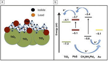
One interesting option could be a combination of NIR QDs with the organometal perovskite to achieve a panchromatic response. Co-sensitization between CH3NH3PbI3 perovskite and PbS QDs in a heterojunction solar cell has been reported Reference Etgar, Gao, Qin, Graetzel and Nazeeruddin32 to obtain a wider wavelength response from the visible to NIR regions. The CH3NH3PbI3 perovskite and the PbS QDs are absorbed on the TiO2 film, when both function simultaneously as light harvester and hole conductor, rendering superfluous the use of an additional HTM.
Figure 4 a shows a scheme for the co-sensitization of CH3NH3PbI3 with PbS QDs on a TiO2 film. Figure 4b shows a schematic energy-level diagram of the hybrid CH3NH3PbI3–PbS QDs heterojunction solar cell. Reference Etgar, Gao, Qin, Graetzel and Nazeeruddin32 The electrons can go into three possible channels upon illumination of this solar-cell structure: (1) electron injection from the PbS QDs to the TiO2, (2) electron transfer from the CH3NH3PbI3 perovskite to the PbS QDs, and (3) electron injection from the CH3NH3PbI3 to the TiO2.
(a) Schematic presentation of the hybrid perovskite—PbS quantum dots heterojunction solar cell. (b) Energy-level diagram of the components involved in the cell. Reprinted with permission from Reference 32. © 2014 Royal Society of Chemistry.

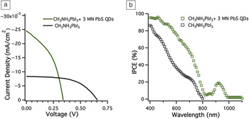
The PV performance shows enhancement of the short-current density (J sc) of the hybrid cell, see Figure 5 a and extended PV response to the NIR region due to the PbS QDs contribution, as shown in the incident photon-to-current efficiency (IPCE) spectra in Figure 5b. Reference Etgar, Gao, Qin, Graetzel and Nazeeruddin32 This hybrid perovskite-QDs solar-cell architecture opens the possibility to take advantage of the high absorption of the perovskite in the visible region and at the same time to get the NIR contribution of the PbS QDs. Future development of the binding between the two light harvesters could result in enhancement of V oc, fill factor, and J sc, expanding possibilities to further increase the efficiency of these solar cells.
(a) Current density–voltage (J–V) measurements of the lead iodide perovskite heterojunction solar cell and the hybrid PbS quantum dots (QDs) lead iodide perovskite heterojunction solar cell. (b) Incident photon to current efficiency (IPCE) of the same heterojunction solar cells. The figure shows the additional contribution of the PbS QDs to the solar-cell current density. Note: MN, monolayer. Reprinted with permission from Reference 32. © 2014 Royal Society of Chemistry.

Chemical modifications of perovskite in HTM-free solar cells
An important property of the organometal perovskite is the ability to tune its optical properties (e.g., bandgap), which is attractive for solar cells. There are two options to change the perovskite bandgap: halide modification and organic cation modification. Although their optical properties are tunable, it is not obvious that these modified perovskites will conduct holes in order to function simultaneously as a light harvester and a hole conductor in HTM-free-based solar cells.
Halide modification
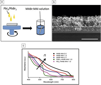
CH3NH3PbI n Br3–n (where 0 ≤ n ≤ 3) was used as a hole conductor and as a light harvester in the solar cell. Reference Aharon, Cohen and Etgar23 CH3NH3PbI n Br3–n was deposited by two-step deposition, as shown in Figure 6 a, separating into two precursors to allow better control of the perovskite composition and efficient tuning of its bandgap. Figure 6b shows a cross-sectional HRSEM figure of the HTM-free CH3NH3PbI n Br3–n solar cell. Various concentrations of methylammonium iodide and methylammonium bromide were studied, revealing that any composition of the hybrid CH3NH3PbI n Br3–n can conduct holes.
(a) Schematic illustration of the two-step deposition technique of the mixed halide perovskite film. (The two-step deposition includes spin coating PbI2 on the electrode followed by dipping in the MAI solution.) MA+ corresponds to CH3NH3 +. (b) High-resolution scanning electron microscopy image of the cross-section of a solar cell discussed in this work. The CH3NH3PbI2Br perovskite can be seen as an overlayer on the TiO2 film. (c) Absorption spectra of the different perovskite compositions. The arrow indicates the increase in n (CH3NH3PbI n Br3–n (where 0 ≤ n ≤ 3)). The absorption of the perovskite can be tuned while changing the I:Br ratio. Reprinted with permission from Reference 23. © 2014 American Chemical Society. Note: FTO, fluorine-doped tin oxide; MAI, methylammonium iodide. The scale bar is 2 μm.

Figure 6c presents the absorption spectra of the various perovskite compositions. The bandgaps are tuned between 1.51 eV (pure CH3NH3PbI3) to 2.12 eV (pure CH3NH3PbBr3). In order to achieve the bandgaps in this region, methylammonium bromine and methylammonium iodine concentrations were changed in the dipping solution. Each of the hybrid perovskites is suitable for hole-conductor-free solar cells, since the conduction band position is higher than the TiO2 conduction band, and the valence band position is lower than the gold work function.
The hybrid iodide/bromide perovskite hole-conductor-free solar cells Reference Aharon, Cohen and Etgar23 show very good stability, with a PCE of 8.54% under 1 sun illumination with a current density of 16.2 mA/cm2. These results suggest the possibility of a graded structure of perovskite solar cells without the need for a hole conductor.
Organic cation modification
Another possibility for chemical modification is to change the organic cation. In particular, by changing the cation from methylammonium (CH3NH3 +, MA+) to a larger formamidinium (NH2CH = NH2 +, FA+) cation, the bandgap of the perovskite decreases, as also supported by the higher Goldschmidt tolerance factor (determines the distortion and the stability of the perovskite structure; expected value of 0.9 to 1 for cubic structure) in the case of the FA+ cation. Reference Lv, Pang, Zhou, Padture, Hu, Wang, Zhou, Zhu, Zhang and Cui33 Formamidinium lead iodide (FAPbI3) and a mixture of methylammonium lead iodide (MAPbI3) and FAPbI3 were studied in hole-conductor-free-based solar cells. Reference Aharon, Dymshits, Rotem and Etgar34 These types of perovskites function both as a light harvester and as a hole conductor in the solar cell.
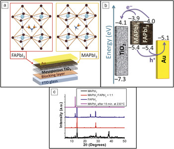
Figure 7 a shows the structure of the hole-conductor-free perovskite solar cell composed of fluorine-doped TiO2 glass/TiO2 compact layer/mesoporous TiO2/perovskite/gold. A schematic illustration of the energy-level diagram is shown in Figure 7b; electron injection and hole transport are possible for the three perovskite compositions: MAPbI3, FAPbI3, and MAPbI3:FAPbI3. During illumination, electrons are injected into the mesoporous TiO2 from the perovskite, whose holes are transported to the metal contact. Figure 7c shows x-ray diffraction (XRD) spectra of the three perovskites. The XRD spectrum of the mixture shows peaks from both MAPbI3 and FAPbI3, indicating that a mixture of the two samples was formed. Reference Aharon, Dymshits, Rotem and Etgar34
The structure of the cell: fluorine-doped tin oxide (FTO) glass/blocking layer (compact TiO2)/mesoporous TiO2/hybrid organic–inorganic perovskite/gold. (a) The layer of perovskite contains MAPbI3, FAPbI3, or a mixture of both. The colors in the crystalline structures represent Pb (light blue), iodide (brown), carbon (dark blue), nitrogen (orange), and hydrogen (white). (b) Energy levels of the different layers of the cell. Reference Kojima, Ikegami, Teshima and Miyasaka1,Reference Dymshits, Rotem and Etgar31 (c) X-ray diffraction (XRD) of the different samples: MAPbI3, MAPbI3:FAPbI3 = 1:1, FAPbI3, and MAPbI3 after 15 min at 230°C. All XRD spectra confirm the crystallographic structure of the different perovskites. Reprinted with permission from Reference 34. © 2015 Royal Society of Chemistry. Note: MA, methylammonium; FA, formamidinium.

Several conclusions can be drawn from this work: (1) Perovskites with different cations can function as a light harvester and as a hole conductor in the solar cell. (2) Surface photovoltage spectroscopy, not shown here, revealed p-type behavior of the different perovskites in the HTM-free solar-cell structure. (3) The PV parameters for the pure MAPbI3 and FAPbI3 solar cells show better stability at high temperature compared to their mixture. (4) The diffusion length is weakly dependent on the light intensity for the different cations (MAPbI3, FAPbI3, and their mixture).
Contacts for HTM-free perovskite solar cells
Since HTM-free perovskite solar cells do not include a HTM, there is direct contact between the perovskite and the back contact. Therefore, this interface has more influence on the PV performance as compared to the HTM. In standard perovskite solar cells (with HTM), the perovskite/contact interface does not exist. Moreover, in most cases when changing the back contact of these standard cells, the PV performance of the solar cell is not affected.
Recently, Mei et al. Reference Mei, Li, Liu, Ku, Liu, Rong, Xu, Hu, Chen, Yang, Grätzel and Han27 fabricated a solar cell that uses a double layer of mesoporous TiO2 and ZrO2 as a scaffold infiltrated with the perovskite and does not require a hole-conducting layer. The perovskite used in this work was (5-AVA) x (MA)1–x PbI3, where 5-AVA corresponds to 5-ammoniumvaleric acid iodide. The researchers drop cast the perovskite through a porous carbon film. This unique type of perovskite results in longer exciton lifetime and higher quantum yield when compared to MAPbI3. A PCE of 12.8% was achieved with stability for over 1000 hours under ambient air. Reference Mei, Li, Liu, Ku, Liu, Rong, Xu, Hu, Chen, Yang, Grätzel and Han27
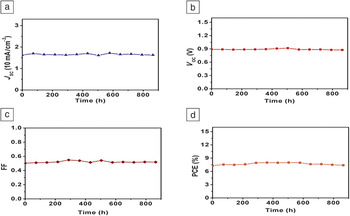
In another work, Reference Zhang, Yang, Wang, Cheng, Zhao and Sun35 a carbon paste was developed and used for the contact in the HTM-free perovskite architecture; a low-temperature process was used, achieving 8.31% efficiency where the carbon electrode was fabricated by a doctor-blading technique. Over 800 hours of stability were demonstrated at ambient atmosphere and room temperature ( Figure 8 ).
Long-term stability of the cell stored in ambient atmosphere at room temperature without encapsulation and measured under 1 sun illumination. (a) The stability of J sc for more than 800 h, (b) the stability of V oc for more than 800 h, (c) the stability of fill factor (FF) for more than 800 h, and (d) the stability of the power conversion efficiency (PCE) for more than 800 h. These graphs show the stability of all the photovoltaic parameters of this solar cell for more than 800 h. Reprinted with permission from Reference 35. © 2014 American Chemical Society. Note: J sc, short-circuit current density; V oc, open-circuit voltage.

Additional work using low-cost carbon electrodes has been reported. Reference Zhou, Shi, Dong, Zhang, Xing, Wang, Du and Ma36 The carbon electrodes in this case were deposited at low temperature on top of the MAPbI3 layer and demonstrated 9% efficiency with over 2000 hours of stability in the dark. The fabrication of HTM-free perovskite solar cells with high stability using carbon electrodes reduces the cost of the solar cell and simplifies its fabrication.
Fully printable mesoscopic perovskite solar cells with a carbon counter electrode using FAPbI3 were introduced into HTM-free solar cells in another study. Reference Hu, Liu, Mei, Yang, Liu and Han37 An efficiency of 11.9% was achieved for the FAPbI3 cells, higher than that for the MAPbI3 cells, with efficiency of 11.4%.
Recently, a gas–solid crystallization process was developed to create pinhole-free perovskite films. Reference Hao, Stoumpos, Liu, Chang and Kanatzidis38 This pinhole-free perovskite film was used in a HTM-free perovskite solar cell demonstrating 10.6% efficiency with good reproducibility. The quality of the pinhole-free perovskite film has an important effect on the interface of the back contact/perovskite or the back contact/metal oxide interface. Consequently, the perovskite film quality improved the PV performance of this solar-cell architecture. These reports demonstrate the importance of the back contact in HTM-free perovskite solar cells and introduce the possibility of further reducing the cost and enhancing the stability of these HTM-free cells.
Summary
This article overviews an unusual solar-cell architecture, in which the active material—organometal perovskite—functions as a light harvester and as a hole conductor, while eliminating the use of a HTM. The elimination of using a HTM could enhance the stability, reduce the cost, and increase the fabrication reproducibility of solar cells. A depletion region was observed in these HTM-free cells, shedding light on its mechanism, and a high open-circuit voltage even without a HTM was demonstrated. Perovskites with chemical modifications were shown to have the duality property required for the HTM-free cells, and a panchromatic response was shown in perovskite QD HTM-free cells. Finally, the role of the back contact in these HTM-free cells was discussed.
The possibility of fabricating a solar cell without the important HTM component and still achieving high PV performance is interesting and important. This needs to be further explored to better understand the material properties and the solar-cell mechanism. To address this, near-term research should focus on the careful design of the metal contact and perovskite interface, which is a key parameter in increasing the PV performance of these unique solar cells. From a technological point of view, this solar-cell structure has an even higher potential impact over the long term than the “standard” configuration involving the HTM.
Acknowledgments
L.E. thanks the Israel Alternative Energy Foundation (I-SAEF) that financed parts of this research, the Ministry of Industry Trade and Labor Office of the Chief Scientist Kamin project N0.50303, and the Tashtiot project of the Office of the Chief Scientist. The author would like to thank the students who worked on these results: S. Aharon, S. Gamliel, A. Dymshits, A. Rotem, B.E Cohen, T. Englman, and M. Koolyk.