1. INTRODUCTION
Nanosecond and subnanosecond diffuse discharges in air and other gases at atmospheric pressure in an inhomogeneous electric field have drawn much attention in recent years (see, e.g., Edited Collection by Tarasenko, Reference Tarasenko2014, and references therein). The diffuse form of discharge in an inhomogeneous electric field at elevated pressures owes to the generation of runaway electrons and X-rays (Tarasova et al., Reference Tarasova, Khudyakova, Loiko and Tsukerman1974; Tarasenko et al., Reference Tarasenko, Orlovskii and Shunailov2003, Reference Tarasenko, Baksht, Burachenko, Kostyrya, Lomaev and Rybka2008a; Baksht et al., Reference Baksht, Burachenko, Kostyrya, Lomaev, Rybka, Shulepov and Tarasenko2009; Levko et al., Reference Levko, Krasik and Tarasenko2012). This type of discharge was given the name a runaway electron preionized diffuse discharge or shortly REP DD (Baksht et al., Reference Baksht, Burachenko, Kostyrya, Lomaev, Rybka, Shulepov and Tarasenko2009). Research in this type of discharge and in the generation of a supershort avalanche electron beam (SAEB), as proposed elsewhere (Tarasenko et al., Reference Tarasenko, Baksht, Burachenko, Kostyrya, Lomaev and Rybka2008a, Reference Tarasenko, Baksht, Burachenko, Kostyrya, Lomaev and Rybkab), gave an unexpected result: A backward beam of fast electrons was detected downstream of a grid cathode (Tarasenko et al., Reference Tarasenko, Baksht, Burachenko, Kostyrya, Lomaev and Rybka2010).
Time-resolved studies, including those with picosecond resolution, show that the current of backward fast electrons downstream of the cathode depends strongly on the anode material (Baksht et al., Reference Baksht, Kozyrev, Kostyrya, Rybka and Tarasenko2013; Kostyrya et al., Reference Kostyrya, Rybka, Tarasenko, Kozyrev and Baksht2013; Tarasenko et al., Reference Tarasenko, Baksht, Burachenko, Kostyrya, Lomaev and Rybka2010, Reference Tarasenko, Baksht, Erofeev, Kostyrya, Rybka and Shutko2013). In the same gas diode design, the amplitude of the backward beam current with a tantalum anode is higher than that with an aluminum anode.
Analysis of the available data shows that fast electrons moving backward through a grid cathode were detected for the first time in helium and neon at low pressure and voltage of several kilovolts applied to the gap (Bokhan & Sorokin, Reference Bokhan and Sorokin1985a, Reference Bokhan and Sorokinb). Two beams of fast electrons were observed in the gap: One beam moved through the grid anode and the other moved backward through the grid cathode. For the gap 0.5 mm, the limiting pressure at which the backward beam was detected was 38 Torr for neon and 90 Torr for helium. The phenomenon was explained by ion injection from the gap through the grid cathode.
At the same time, the generation of a backward runaway electron beam (BRAEB) in atmospheric pressure air was also detected within less than 0.5 ns after applying a voltage pulse of higher amplitude and shorter risetime (Baksht et al., Reference Baksht, Kozyrev, Kostyrya, Rybka and Tarasenko2013; Kostyrya et al., Reference Kostyrya, Rybka, Tarasenko, Kozyrev and Baksht2013; Tarasenko et al., Reference Tarasenko, Baksht, Burachenko, Kostyrya, Lomaev and Rybka2010, Reference Tarasenko, Baksht, Erofeev, Kostyrya, Rybka and Shutko2013). The so short time left almost no chance for ions to move and more so to be injected into the region downstream of the grid cathode. According to research data, the angle of electron beam generation in atmospheric pressure air under similar conditions was higher than 2π (Tarasenko et al., Reference Tarasenko, Baksht, Burachenko, Kostyrya, Lomaev and Rybka2008a, Reference Tarasenko, Baksht, Burachenko, Kostyrya, Lomaev and Rybkab). However, the above data were obtained on pulsers with negative polarity, making impossible the arrangement of a collector downstream of the high-voltage cathodes.
The foregoing suggests that BRAEBs can be generated in helium and neon at a pressure of tens of Torr (Bokhan & Sorokin, Reference Bokhan and Sorokin1985a, Reference Bokhan and Sorokinb) and in air at atmospheric pressure (Baksht et al., Reference Baksht, Kozyrev, Kostyrya, Rybka and Tarasenko2013; Kostyrya et al., Reference Kostyrya, Rybka, Tarasenko, Kozyrev and Baksht2013; Tarasenko et al., Reference Tarasenko, Baksht, Burachenko, Kostyrya, Lomaev and Rybka2010, Reference Tarasenko, Baksht, Erofeev, Kostyrya, Rybka and Shutko2013). However, the conditions for the generation of a backward beam in atmospheric pressure air and its parameters are poorly understood and so is the mechanism of the phenomenon.
The present paper studies the conditions under which a BRAEB is generated in air through a grid cathode for which we use different cathode designs and anodes made of Al, Ta, and stainless steel. The backward beam current and X-ray exposure dose are measured with nanosecond and picosecond resolution. The study continues our research reported elsewhere (Baksht et al., Reference Baksht, Kozyrev, Kostyrya, Rybka and Tarasenko2013; Kostyrya et al., Reference Kostyrya, Rybka, Tarasenko, Kozyrev and Baksht2013; Tarasenko et al., Reference Tarasenko, Baksht, Burachenko, Kostyrya, Lomaev and Rybka2010, Reference Tarasenko, Baksht, Erofeev, Kostyrya, Rybka and Shutko2013). Note that we have not managed to find any other papers which report on the generation of BRAEBs in air and other gases at atmospheric pressure.
2. EXPERIMENTAL SETUP AND MEASURING TECHNIQUE
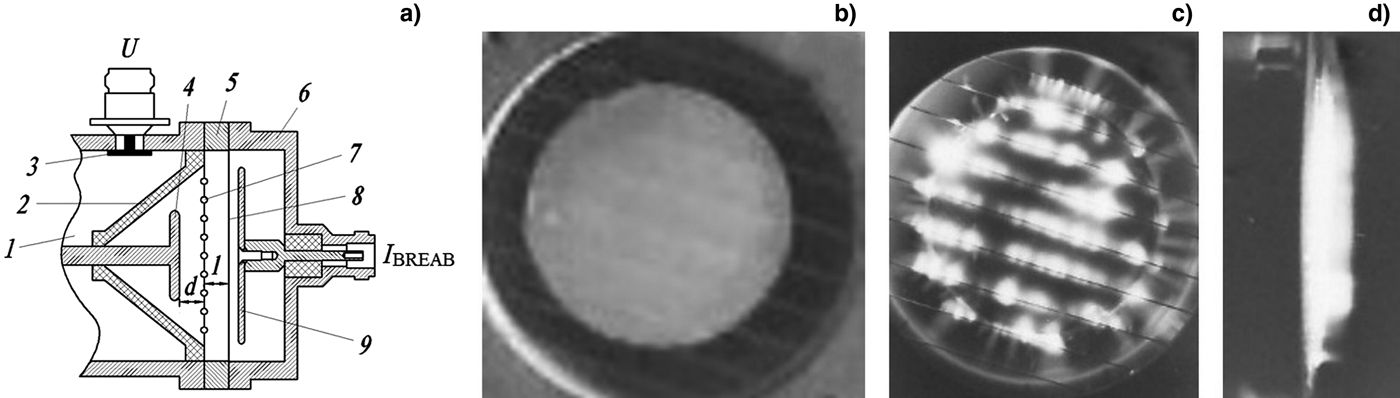
In our experiments, we used a SLEP-150 pulser capable of producing voltage pulses of negative and positive polarity (Tarasenko et al., Reference Tarasenko, Kostyrya, Baksht and Rybka2011; Kostyrya et al., Reference Kostyrya, Rybka and Tarasenko2012) at negative polarity, a SAEB with ~6·1010 electrons was detected in atmospheric pressure air downstream of an Al foil anode 10-µm-thick (Kostyrya et al., Reference Kostyrya, Rybka and Tarasenko2012). For the generation of a BRAEB, a voltage pulse of positive polarity with an amplitude of ≅150 kV and full width at half maximum (FWHM) of ≅1 ns was applied to the high-voltage electrode of a gas diode. The voltage risetime was determined by a peaking switch and was ≅0.3 and ≅0.4 ns at negative and positive polarity, respectively. Figure 1a shows a schematic of the gas diode with a collector for operation with voltage pulses of positive polarity.
Gas diode and measuring system (a): 1 – coaxial line, 2 – insulator, 3 – capacitive voltage divider, 4 – anode, 5 – steel ring, 6 – collector box, 7 – wire grid, 8 – foil, and 9 – collector receiving part of diameter 56 mm. Images of the gas diode in a pulse without the collector, metal ring, and foil: View from the grid cathode (b, c) and side view (d) with no discharge plasma (b) and with (c, d); the anode diameter is 38 mm, the wire separation is 4 mm.

The anode of the gas diode was 38 mm in diameter and represented a flat disk 3 mm thick with rounded edges. The anode side facing the cathode was made of aluminum, stainless steel or tantalum. The cathode (7) was a grid of parallel steel wires of diameter 0.2 or 0.4 mm stretched with a step of 3, 4, 6 or 8 mm on a flat steel ring 3 mm thick. Additionally, we used grid cathodes made of wire of diameter 0.4 mm with square meshes of size 2 × 2 and 1 × 1 mm2, a tube cathode from foil, and a needle cathode. The steel ring (5) had a hole of diameter 62 mm at its center and was fixed to the flange of the gas diode. On the other side of the ring there was an Al foil of thickness 10 µm reinforced with a grid of transparency 90%. For measuring the electron beam, different collectors were placed downstream of the foil (8) which was also fixed to the flange of the gas diode. The grid-cathode (7) and the foil (8) were spaced by 3 mm, but their separation could be changed to 6, 9, and 12 mm by using additional rings.
The total number of electrons was measured using the collector with a receiving part of diameter 56 mm (9) shown in Figure 1a. For measuring the pulse width of the backward beam with picosecond and subnanosecond resolution, a collimator and a diaphragm were used. For picosecond measurements, we used a collector with a receiving part of diameter 3 mm and a collimator with a thickness of 5 mm and hole diameter of 1 mm placed downstream of the foil (8). This made it possible to measure beam current pulses with a FWHM of up to 25 ps (Tarasenko et al., Reference Tarasenko, Rybka, Burachenko, Lomaev and Balzovsky2012). Using a collector with a receiving part diameter of 20 mm and a diaphragm with a hole diameter of 18 mm, the time resolution of the measuring system reached 80 ps (Tarasenko, Reference Tarasenko2011). The electron beam attenuation was measured using Al foil filters of different thickness, and the X-ray attenuation using Cu foil filters of different thickness. The filters were placed close to the Al foil through which the backward beam was extracted and were connected to the gas diode case along the entire perimeter.
The electron beam moving forward (SAEB) was recorded at negative polarity. The cathode was a grid of parallel steel wires of diameter 0.2 mm stretched with a step of 4 mm on a flat steel ring of diameter 40 mm. The anode was an Al foil 10 µm thick reinforced with a grid of transparency 90%.
For registration electrical signals with picosecond and subnanosecond resolution, we used a LeCroy WaveMaster 830Zi-A digital real-time oscilloscope (up to 30 GHz, 80 GS/s). The collimator with a 1-mm hole allowed measurements of the runaway electron beam parameters without additional signal attenuators. The X-ray exposure dose was measured with Arrow-Tech dosimeters (Model 138). The dose per pulse was estimated from 50 pulses for the Ta anode, from 100 pulses for the stainless steel anode, and from 200 pulses for the Al anode. Imprints of the electron beam and X-rays were recorded on RF (radiographic film)-3 film. Images of the discharge were taken with a Zenit film camera as viewed from the grounded grid and from its side at positive polarity. The Al foil (8) located downstream of the grid (7) was removed.
3. MEASUREMENT RESULTS
In the study, we measured the BRAEB current (IBRAEB) and X-ray with tantalum, stainless steel, and aluminum anodes and cathodes of different designs. Moreover, the range and number of measured parameters was greatly extended as compared to our previous studies (Baksht et al., Reference Baksht, Kozyrev, Kostyrya, Rybka and Tarasenko2013; Kostyrya et al., Reference Kostyrya, Rybka, Tarasenko, Kozyrev and Baksht2013; Tarasenko et al., Reference Tarasenko, Baksht, Burachenko, Kostyrya, Lomaev and Rybka2010, Reference Tarasenko, Baksht, Erofeev, Kostyrya, Rybka and Shutko2013). The BRAEB and X-rays were measured at positive polarity, and the SAEB at negative polarity of the SLEP-150 pulser. Before measurements, each fresh electrode was conditioned by several tens of pulses.
Figure 2 shows waveforms of the voltage from the capacitive voltage divider shown in Figure 1 and waveforms of the backward beam for the Ta and Al anodes at picosecond and subnanosecond resolution.
Waveforms of the voltage from the capacitive voltage divider (a, c) and backward beam current at picosecond (b), and subnanosecond (d) resolution for the Ta and Al anodes, grid cathode composed of wires of diameter 0.2 mm spaced by 4 mm, and interelectrode gap 4 mm.
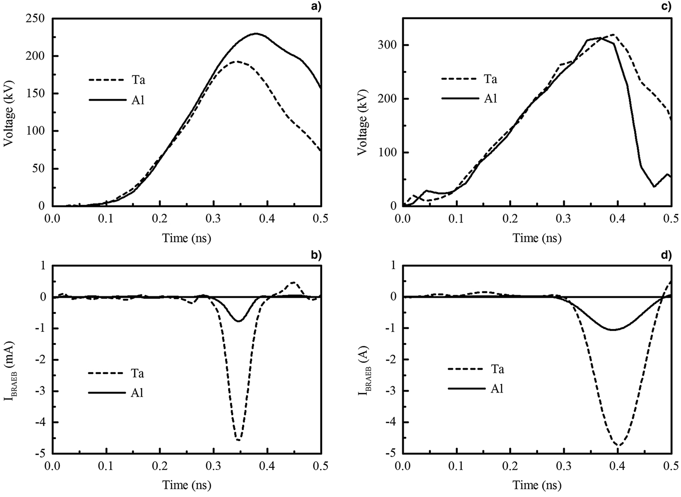
The waveforms of the voltage allow for a 60 ps delay of arrival of the reflected voltage wave at the capacitive voltge divider. The shape and amplitude of voltage pulses varied little with the anode material. The average voltage amplitude in 50 pulses for the Al anode is a mere 10% higher than that for the Ta anode. Note that the amplitude and risetime of the voltage from the capacitive divider at positive polarity were higher than those at negative polarity (SAEB generation), while all other things being equal. This agrees with data on the effect of polarity inversion (Shao et al., Reference Shao, Tarasenko, Zhang, Beloplotov, Yang, Lomaev, Zhou, Sorokin and Yan2014).
At picosecond resolution (Fig. 2b), the BRAEB was measured by the collector with a receiving part diameter of 3 mm through the 1 mm collimator hole. Like in our previous studies (Tarasenko et al., Reference Tarasenko, Baksht, Burachenko, Kostyrya, Lomaev and Rybka2010, Reference Tarasenko, Baksht, Erofeev, Kostyrya, Rybka and Shutko2013; Baksht et al., Reference Baksht, Kozyrev, Kostyrya, Rybka and Tarasenko2013; Kostyrya et al., Reference Kostyrya, Rybka, Tarasenko, Kozyrev and Baksht2013), the amplitude of the backward beam for the Ta anode was much higher than that for the Al anode at the same voltage amplitudes. However, the FWHM of the backward beam with maximum current amplitudes in both cases was about the same, measuring 40–45 ps. Note that the collimator and collector with a receiving part diameter of 3 mm allow one to measure only a small part of the backward beam, and this decreases the current pulse width compared with that from the entire foil surface both for backward beams and for SAEBs (Tarasenko et al., Reference Tarasenko, Skakun, Kostyrya, Alekseev and Orlovskii2004, Reference Tarasenko, Baksht, Burachenko, Kostyrya, Lomaev and Rybka2008a, Reference Tarasenko, Baksht, Erofeev, Kostyrya, Rybka and Shutko2013).
At subnanosecond resolution (Fig. 2d), the backward beam was measured by the collector with a receiving part diameter of 20 mm through the 18 mm diaphragm hole The FWHM of the backward beam for the Ta and Al anodes was ≅95 and ≅115 ps, respectively. The FWHM of the backward beam measured by the collector with a receiving part diameter of 20 mm differed little from the FWHM over the entire surface of the foil (8) in Figure 1, but the number of backward runaway electrons was about two times smaller than their number from the entire foil surface.
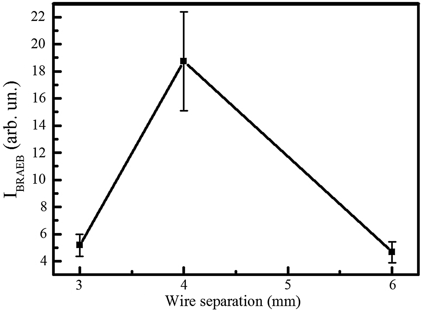
For increasing the backward beam amplitude, the cathode design and the wire separation were optimized (Fig. 3).
Backward beam amplitude versus the wire separation for wires of diameter 0.2 mm.
The highest backward beam amplitude was obtained for the cathode consisting of parallel wires of diameter 0.2 mm spaced by 4 mm. Increasing the wire diameter increased their optimum separation.
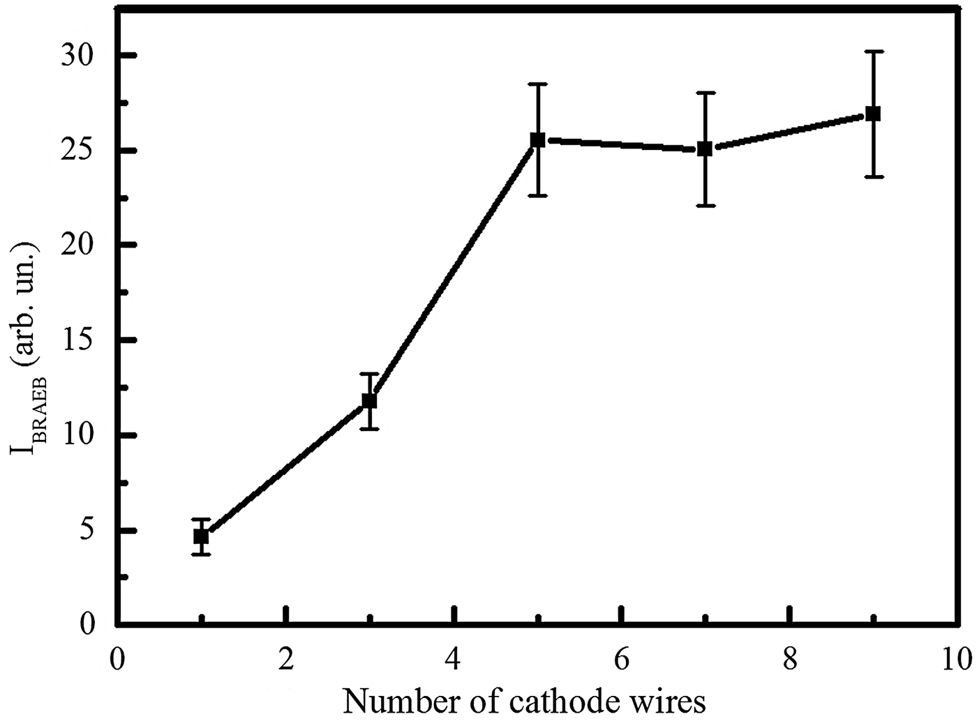
The amplitude of the backward beam depended on the number of parallel wires. Figure 4 shows the beam current amplitude against the number of cathode wires.
Backward beam current versus the number of cathode wires of diameter 0.2 mm.
The first wire was arranged at the center and its length was equal to the diameter of the ring (5) in Figure 1. The next two wires were arranged symmetrically on both sides of the first wire and so were the next two. It is seen from Figure 4 that increasing the number of wires to 5, greatly increased the backward beam amplitude, and further increasing their number caused saturation of the beam amplitude.
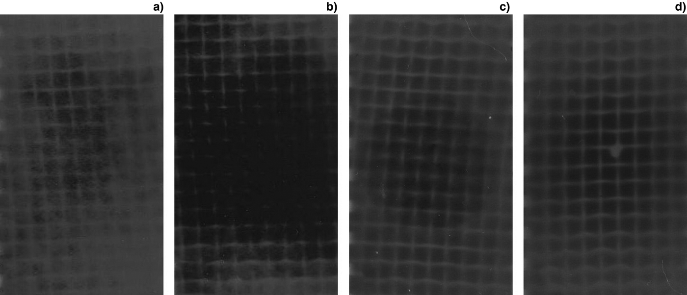
The use of the grid cathode with square meshes and smaller wire separation decreased the backward beam amplitude. For the cathode with a mesh size of 2 × 2 mm2 and wire thickness of 0.4 mm, the number of backward runaway electrons decreased almost ten times. Imprints on the RF-3 film exposed to the backward beam and X-rays for the mesh grid cathode are shown in Figures 5a and 5b.
RF-3 film exposed to the backward beam and X-rays within 5, 10, 50, and 200 pulses for different cathode designs: Grid with a mesh size of 2 × 2 mm2 (a, b); foil ring of diameter 20 mm, height 4 mm, and thickness 100 µm on a grid with a mesh size of 2 × 2 mm2 (c); needle of height 4 mm on a grid with a mesh size of 2 × 2 mm2 (d). The interelectrode distance is 5 (a, b) and 4 mm (c, d).
For all four imprints, the separation between the cathode (7) and foil (8) was l = 3 mm (Fig. 1). The RF-3 film in a black paper envelope of thickness 120 µm was placed downstream of the foil. All imprints reveal a clearly defined grid structure. With the cathode comprising only a grid, several pulses were sufficient for noticeable blackening of the film. At the same number of pulses, the highest degree of blackening was observed when the backward beam amplitude was highest. With the cathode comprising wires of diameter 0.2 mm spaced from each other and from the Ta anode by 4 mm, the blackening of the film was maximal. A single pulse was sufficient for total film exposure. The number of backward runaway electrons, in this case, was ~7·109.
The imprint shown in Figure 5c was obtained with a cathode representing a ring of diameter 20 mm, height 4 mm, and wall thickness 100 µm placed on a grid with a mesh size of 2 × 2 mm2 facing the anode. With this cathode at a ring–anode separation of 4 mm, the amplitude of the backward beam decreased 3.7 times compared with that in Figures 5a and 5b. At the center of the imprint, one can see severe ring-shaped blackening of the film.
The imprint in Figure 5d was obtained with a cathode representing a sewing needle of height 4 mm. With this cathode, the amplitude of the backward runaway beam decreased greatly such that the beam was hardly detectable against the background of electromagnetic noise. In this case, to obtain a clear imprint, the exposure was increased to 200 pulses. At the center of the imprint, one can see a bright spot which shows the position of the needle cathode. It can be supposed that the main film exposure for the ring and needle cathodes owes mostly to bremsstrahlung X-rays from the anode. Earlier studies also revealed a decrease in SAEB amplitude for a needle cathode compared with tubular and spherical cathodes (Tarasenko et al., Reference Tarasenko, Skakun, Kostyrya, Alekseev and Orlovskii2004). Increasing the number of runaway electrons requires a longer sharp edge of the cathode with a small curvature radius (Tarasenko, Reference Tarasenko2011; Kostyrya et al., Reference Kostyrya, Rybka and Tarasenko2012) without any mutual shielding from adjacent wires.
With the grid in which the mesh size was 1 × 1 mm2, no backward electron beam was detected. The same was observed when the foil (8) was brought close to the grid (7). This can be explained by a decrease in electric field strength near the close-spaced grid wires as the grid–foil separation is decreased.
At increasing distance between cathode (wire grid) and collector through both increasing distance between cathode (7) and foil (8) or moving of the collector away from the foil (8) with keeping of distance between cathode (7) and foil (8) at 3 mm, the number of backward runaway electrons decreased.
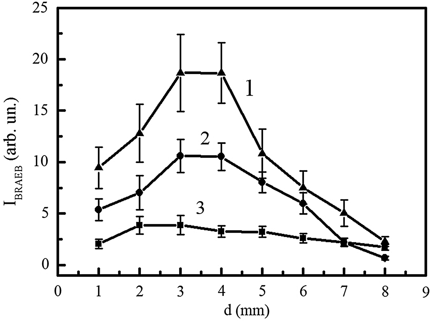
Figure 6 shows dependencies of the number of backward electrons on the interelectrode distance in a discharge in atmospheric pressure air.
Number of backward electrons versus the interelectrode distance in a discharge in atmospheric pressure air with the cathode consisting of wires of diameter 0.2 mm spaced by 4 mm for the anodes made of tantalum – 1, stainless steel – 2, and aluminum – 3.
The dependencies were obtained using the collector with a receiving part diameter of 56 mm. The use of the collector distorted the pulse shape of the beam current but allowed us to determine the number of electrons downstream of the entire foil surface. For all anode materials, there exists an optimum interelectrode distance at which the highest number of runaway electrons is detected downstream of the cathode. The number of backward electrons for the stainless steel anode is higher than that for the Al anode but lower than their number for the Ta anode. This fits the ratio of atomic numbers for these materials. The largest number of backward electrons was detected for the Ta anode and was ~7·109, which agrees with data of our previous studies (Baksht et al., Reference Baksht, Kozyrev, Kostyrya, Rybka and Tarasenko2013; Kostyrya et al., Reference Kostyrya, Rybka, Tarasenko, Kozyrev and Baksht2013; Tarasenko et al., Reference Tarasenko, Baksht, Erofeev, Kostyrya, Rybka and Shutko2013). The number of backward electrons under optimum conditions was an order of magnitude lower than that of SAEB electrons with optimum cathode and gas diode designs at negative polarity; the number of SAEB electrons downstream of the anode was 6.2·1010 in a pulse (Kostyrya et al., Reference Kostyrya, Rybka and Tarasenko2012). The maximum in the energy distribution of the backward runaway beam was lower than that in the SAEB distribution, as was the case in our previous studies (Baksht et al., Reference Baksht, Kozyrev, Kostyrya, Rybka and Tarasenko2013; Kostyrya et al., Reference Kostyrya, Rybka, Tarasenko, Kozyrev and Baksht2013; Tarasenko et al., Reference Tarasenko, Baksht, Erofeev, Kostyrya, Rybka and Shutko2013). The maximum energy of the backward beam was lower than the maximum SAEB energy. The electron energy in gas diodes at voltage pulses of negative polarity was studied in detail elsewhere (Tarasenko et al., Reference Tarasenko, Shpak, Shunailov and Kostyrya2005, Reference Tarasenko, Baksht, Burachenko, Kostyrya, Lomaev and Rybka2008a, Reference Tarasenko, Baksht, Burachenko, Kostyrya, Lomaev and Rybkab, Reference Tarasenko, Kostyrya, Baksht and Rybka2011; Mesyats et al., Reference Mesyats, Reutova, Sharypov, Shpak, Shunailov and Yalandin2011; Alekseev et al., Reference Alekseev, Baksht, Boichenko, Kostyrya, Tarasenko and Tkachev2012; Zhang et al., Reference Zhang, Tarasenko, Shao, Beloplotov, Lomaev, Sorokin and Yan2014; Kozyrev et al., Reference Kozyrev, Kozhevnikov, Vorobyev, Baksht, Burachenko, Koval and Tarasenko2015).
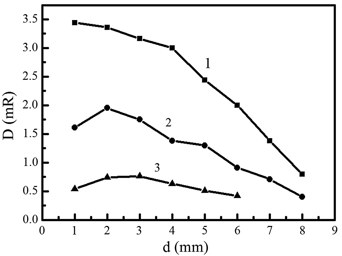
Figure 7 shows dependencies of the X-ray exposure dose on the interelectrode distance in a discharge in atmospheric pressure for different anode materials.
X-ray exposure dose produced by the backward beam versus the interelectrode distance for the Ta anode – 1, stainless steel anode – 2, and Al anode – 3. The cathode consists of wires of diameter 0.2 mm spaced by 4 mm.
As expected, the maximum exposure doses were obtained for the Ta anode. However, the maximum doses were produced with smaller interelectrode distances than those at which the number of backward electrons was maximal. This result differs from data on the interelectrode distance dependence of SAEB and X-rays produced at negative polarity of the SLEP-150 pulser (Alekseev et al., Reference Alekseev, Baksht, Boichenko, Kostyrya, Tarasenko and Tkachev2012). When the SLEP-150 pulser operates at negative polarity, the X-rays are produced due to electron bombardment of a foil anode made of metal with a high atomic number and are extracted through the same foil anode. This causes substantial attenuation of low-energy X-ray quanta. When the SLEP-150 pulser operates at positive polarity, the X-rays are also produced on deceleration of fast electrons at a metal anode with a high atomic number but their extraction from the gas diode is through a thin Al foil. This reduces the absorption of soft X-rays. The decrease in X-ray absorption together with an increase in gap voltage at positive polarity made it possible to increase the X-ray dose in a pulse several times (to 3.5 mR).
4. DISCUSSION
The reported research results confirm the possibility of generation of a BRAEB and the main trends of this interesting phenomenon detected in atmospheric pressure air (Baksht et al., Reference Baksht, Kozyrev, Kostyrya, Rybka and Tarasenko2013; Kostyrya et al., Reference Kostyrya, Rybka, Tarasenko, Kozyrev and Baksht2013; Tarasenko et al., Reference Tarasenko, Baksht, Burachenko, Kostyrya, Lomaev and Rybka2010, Reference Tarasenko, Baksht, Erofeev, Kostyrya, Rybka and Shutko2013). By optimizing the cathode design and interelectrode gap we have managed to increase the X-ray dose at positive polarity to 3.5 mR. It is found that the generation of backward beams with highest amplitudes requires cathodes composed of wires spaced by ≥4 mm.
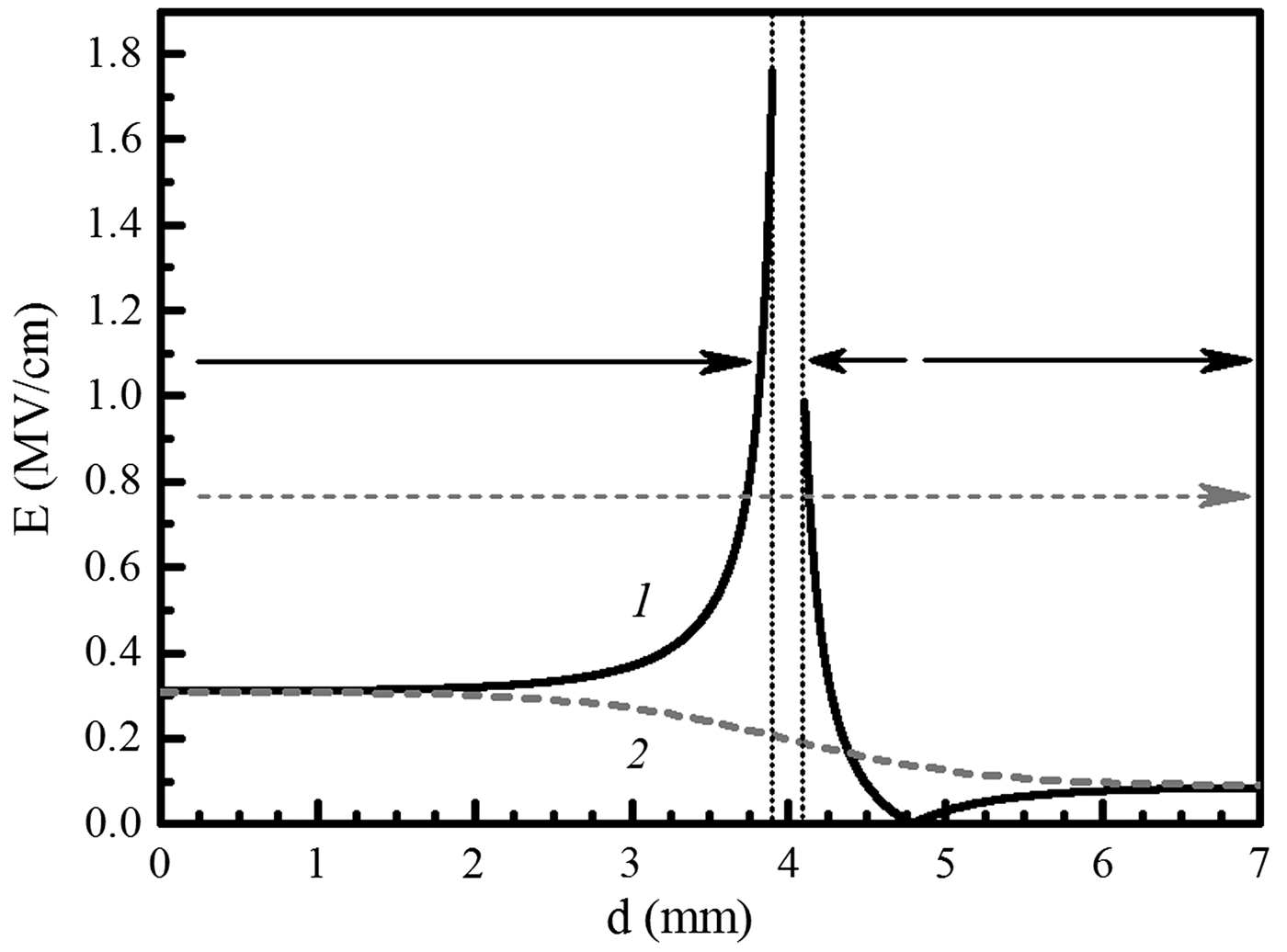
The main question to be answered is the cause of appearance of runaway electrons downstream of the cathode. Reasoning from the fact that the electric field penetrates into this cathode region (Baksht et al., Reference Baksht, Kozyrev, Kostyrya, Rybka and Tarasenko2013; Kostyrya et al., Reference Kostyrya, Rybka, Tarasenko, Kozyrev and Baksht2013; Tarasenko et al., Reference Tarasenko, Baksht, Erofeev, Kostyrya, Rybka and Shutko2013), let us elucidate whether its value is high enough for electron runaway. For this purpose, we calculated the distribution of the electric field strength in the gap along the line near its symmetry axis. The simulation was performed using an ELCUT 5.1 Professional program (http://elcut.ru/allnews/elcut51_r.htm). The calculation results are presented in Figure 8.
Electric field strength distribution between the anode (at the left) and grounded foil (at the right) along the line passing through the wire – 1 and between the wires – 2 near the gap symmetry axis. The wire boundaries are marked by vertical dotted lines; the direction of the field vector is indicated by arrows. The interelectrode distance and the wire separation is 4 mm.
From the calculations it follows that the maximum electric field strength is observed on the region near the wire surface and its value under these conditions is higher than 1 MV cm−1. The so high electric field explains the appearance of first electrons at the cathode, including the wire side opposite the anode (between the grid and the foil) and the transition of part of the electrons to the runaway mode. However, this is insufficient for the number of backward electrons to be large. The high electric field between the grid and foil provides the generation of first runaway electrons. The generation of a considerable number of electrons (~7·109 for the Ta anode) requires an ionization wave front moving from the wire cathode backward to its downstream region as well as toward the anode.
Figure 1 shows images of the gas diode without the collector, metal ring, and foil as viewed from the grid cathode (Figs. 1b and 1c) and from its side (Fig. 1d) with no discharge plasma (Fig. 1b) and with the plasma in a pulse at positive polarity (Figs. 1c and 1d). It is seen that the dense plasma glows at the cathode wires (Fig. 1c) and that the radiation is detected downstream of the cathode at a distance of about 10 mm from the ring to which the cathode wires are attached (Fig. 1d). These images confirm the backward ionization wave propagation. Most of the runaway electrons are generated at the ionization wave front (Tarasenko et al., Reference Tarasenko, Orlovskii and Shunailov2003, Reference Tarasenko, Baksht, Burachenko, Kostyrya, Lomaev and Rybka2008a, Reference Tarasenko, Baksht, Burachenko, Kostyrya, Lomaev and Rybkab, Reference Tarasenko, Baksht, Burachenko, Kostyrya, Lomaev and Rybka2010; Baksht et al., Reference Baksht, Burachenko, Kostyrya, Lomaev, Rybka, Shulepov and Tarasenko2009; Tarasenko, Reference Tarasenko2011; Kostyrya et al., Reference Kostyrya, Rybka and Tarasenko2012; Shao et al., Reference Shao, Tarasenko, Zhang, Baksht, Yan and Shut'ko2012, Reference Shao, Tarasenko, Zhang, Burachenko, Rybka, Kostyrya, Lomaev, Baksht and Yan2013; Zhang et al., Reference Zhang, Tarasenko, Shao, Baksht, Burachenko, Yan and Kostyray2013, Reference Zhang, Tarasenko, Shao, Beloplotov, Lomaev, Sorokin and Yan2014).
Surely, the radiation from the dense plasma is more intense mostly in the gap between the grid cathode and plane anode. Hence, the number of runaway electrons in the gap is much larger and their energy is higher than that of backward electrons. When the potential electrode is the anode, it is very difficult to detect a SAEB. The generation of a SAEB with a large number of runaway electrons can be judged from intense (up to 3.5 mR) X-rays from the anode. However, when the pulser polarity is reversed with replacement of the plane potential anode by the grid cathode and also the mesh cathode by the Al foil of thickness 10 µm, which becomes the anode, stable SAEB generation is observed. The SAEB amplitude in atmospheric pressure air reaches 100 A at a FWHM of ~100 ps which corresponds to 6.2·1010 fast electrons in a pulse (Kostyrya et al., Reference Kostyrya, Rybka and Tarasenko2012).
As it follows from Figures 6 and 7, the number of backward runaway electrons and X-ray exposure doses depend largely on the anode material. The use of a metal anode with a large atomic number increases the number of backward electrons and the X-ray exposure dose. The increase in the exposure dose owes to an increase in bremsstrahlung X-ray intensity generated by runaway electrons accelerated between the grid cathode and anode with a large atomic number. We suppose that the increase in the number of backward runaway electrons, in this case, is due to participation of bremsstrahlung X-rays from the anode in the formation of an ionization wave whose front moves backward and to additional electron emission from the cathode wires. Apparently, the X-rays from the anode are significant in early stage of the formation of dense plasma at the cathode when the number of backward runaway electrons is small. According to the data of our studies, it can be stated that most of the runaway electrons at a subnanosecond voltage pulse risetime is generated due to electric field strength amplification near the polarized ionization wave front (Tarasenko et al., Reference Tarasenko, Orlovskii and Shunailov2003, Reference Tarasenko, Baksht, Burachenko, Kostyrya, Lomaev and Rybka2008a, Reference Tarasenko, Baksht, Burachenko, Kostyrya, Lomaev and Rybkab, Reference Tarasenko, Baksht, Burachenko, Kostyrya, Lomaev and Rybka2010, Baksht et al., Reference Baksht, Burachenko, Kostyrya, Lomaev, Rybka, Shulepov and Tarasenko2009; Tarasenko, Reference Tarasenko2011; Kostyrya et al., Reference Kostyrya, Rybka and Tarasenko2012; Shao et al., Reference Shao, Tarasenko, Zhang, Baksht, Yan and Shut'ko2012, Reference Shao, Tarasenko, Zhang, Burachenko, Rybka, Kostyrya, Lomaev, Baksht and Yan2013; Zhang et al., Reference Zhang, Tarasenko, Shao, Baksht, Burachenko, Yan and Kostyray2013, Reference Zhang, Tarasenko, Shao, Beloplotov, Lomaev, Sorokin and Yan2014).
5. CONCLUSION
The results reported in the paper confirm the possibility of generation of a backward runaway electron beam. It is found that the highest amplitudes of the backward beam are attained using a plane anode made of metal with a high atomic number, in our experiments, tantalum. It is shown that the optimum interelectrode distance for the generation of backward beams are larger than those for the generation of maximum exposure doses. The generation of backward runaway electrons owes to electric field penetration through the widely spaced grid and backward propagation of the dense plasma due to electric field amplification near the grid cathode with a small curvature radius. It is supposed that preionization of the region ahead of the backward dense plasma front by bremsstrahlung X-rays from the anode influences the amplitude of the backward beam.
ACKNOWLEDGEMENT
The work is performed in the framework of the Russian Science Foundation (the project #14-29-00052).