Introduction: Metrics of ion source performance
Focused ion beam (FIB) instruments serve a variety of distinct applications, and their capabilities depend very much upon their underlying ion source technology. Ion source technologies are characterized by the available ion species, emission stability, the beam current that can be attained within a given focused probe, and the size of the focused probe. The latter two characteristics rely critically upon the ion source’s reduced brightness (measured in Am–2sr–1V–1) and the energy spread (measured in eV). For each of the ion sources reviewed in this article, these characteristics will be presented. For reference and comparison, the most widely used FIB source, the gallium liquid metal ion source (LMIS), is characterized as follows: The ion species available with the LMIS is principally gallium, and through active control schemes, such an ion source can be relatively steady for periods up to several days—depending on the usage. The reduced brightness of the gallium LMIS is usually cited as 106 Am–2sr–1V–1, and the energy spread is about 5 eV. Reference Forbes, Mair and Orloff1 Conventionally, a gallium FIB system can achieve a small focused probe size of 5 nm or less when small currents of 1 pA are required. Focused beams with higher currents of 1 nA can be achieved with a larger probe size of 40 nm. The gallium LMIS is a mature technology with a variety of well-established FIB applications; whereas the three technologies reviewed in the following three sections are less mature and are just now gaining commercial acceptance.
Inductively coupled plasma ion sources
Theory of operation
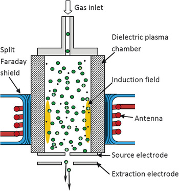
A cross-sectional schematic view of an inductively coupled plasma (ICP) ion source is shown in Figure 1 .The cylindrical plasma chamber has a solenoid antenna wrapped around its outside, and a Faraday shield is positioned between the antenna and the plasma chamber.
Schematic of an inductively coupled plasma source.

A radio frequency (RF) current is passed through the antenna in order to create an azimuthal induction field in the outer skin of the plasma that causes plasma electrons to be accelerated. The RF is significantly below the plasma’s electron resonant frequency (a few gigahertz) and usually above the plasma’s ion resonant frequency (a few megahertz) so as to cause the electron population to be heated while the ions remain close to room temperature.
The Faraday shield has a multitude of longitudinal cuts designed to minimize Eddy currents and power loss in the shield while serving to terminate the time-varying electric field created by the voltage that exists on the antenna. Hence, the arrangement minimizes capacitive coupling from the antenna to the plasma while maximizing inductive power coupling.
The induction field accelerates electrons in the outer “skin” of the plasma to a sufficient kinetic energy to cause ionization of the resident gas. This process of creating a plasma can be used for a broad range of plasma gases and has proven able to create plasma densities as high as 1 × 1013 cm–3 (Xe+), resulting in a reduced brightness (energy normalized brightness) for the ion source of 1 × 10⁴ Am–2sr–1V–1. Reference Smith, Tesch, Martin and Kinion2,Reference Smith, Tesch, Martin and Boswell3 The source can operate continuously (provided the gas supply is maintained) due to negligible aging effects in the plasma chamber, providing beam current stability of less than ±0.5% h–1, an axial energy spread of 5 eV (Xe+), and lifetimes in excess of two years.
Applications
Up until the introduction of ICPs, the duoplasmatron had been the brightest and most commonly employed oxygen ion source used for ultralow energy (100 eV) SIMS applications. However, the duoplasmatron has lower brightness, larger energy spread, and a significantly shorter lifetime than the new commercial ICP sources, such that many duoplasmatrons are now being phased out and replaced with ICPs. The enhanced level of performance with ICP O2 + FIBs has provided more than an order of magnitude increase in current density in 100 eV focused O2 + beams, resulting in viable sub-nm depth resolution SIMS analysis of electropositive dopant species used in the semiconductor industry. Reference Merkulov, Peres, Choi, Horreard, Ehrke, Loibl and Schumacher4
For many SIMS applications, negatively charged oxygen ions (O–) are preferred. Reference Hoppe, Cohen and Meibom5 The significantly enhanced brightness and reduced energy spread of the ICP source when compared to the duoplasmatron has reduced the minimum O– spot size from 200 nm to 50 nm, with 1pA at 15 keV.
ICPs are commonly used to create inert gas ions, such as helium, neon, argon, and xenon. These inert gas ion sources are now being used in conjunction with low energy ion scattering spectrometers to deliver helium, neon, and argon beams with sub-5 µm spatial resolution with greater than 1 nA, and 3 keV to 8 keV beam energies. Reference Druce6 For large volume ion beam machining, ICP-produced xenon ions offer the highest sputter yields and the highest current densities.
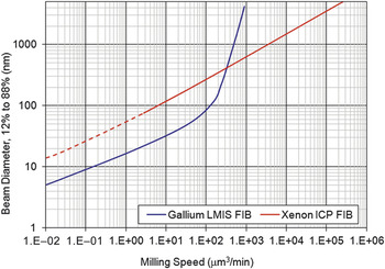
Figure 2 shows the optimum spot size as a function of the milling speed (um Reference Smith, Tesch, Martin and Boswell3 /minute), comparing LMIS (Ga+) and ICP (Xe+) 30 keV focused beams sputtering a silicon substrate at normal beam incidence. At Ga+ beam currents above 6 nA (100 µm3/min in Figure 2), the effective beam brightness (measured at the target) drops precipitously due to the relatively low angular intensity (≈15 μA/sr) of the gallium LMIS, compared to that of the ICP source (≈10 mA/sr).
Spot diameter versus milling speed, while sputtering at normal incidence on silicon. LMIS, liquid metal ion source; FIB, focused ion beam; ICP, inductively coupled plasma.

Current applications for the higher milling speeds provided by the xenon ICP FIB include:
-
1. Large-area cross-sections for failure analysis of semiconductor devices such as bonded wafers, through silicon vias (TSVs), solder balls, and microelectromechanical systems devices. Large-scale cross-sectional analysis of metal samples and geological materials is also possible. Reference Altmann, Klengel, Schischka and Petzold7,Reference Tesch, Smith, Martin and Kinion8
-
2. Micromachining of various micrometer to millimeter scale structures, such as apertures and slits for charged particle beams. In fact, a broad range of machining applications is now possible in situations where laser and/or micro-electric discharge machining are not viable.
-
3. The high beam current that can be achieved with 1–2 μm spot sizes has also proven to be beneficial for some circuit editing applications (e.g., isolating surface antennas on RF chips and cutting trenches to sever sub-surface metal lines), where relatively large volumes of material need to be removed to edit sub-surface features. When micrometer scale editing is required, a xenon ICP FIB can be significantly faster than a low current Ga+ FIB, and offers the additional benefit of not leaving implanted gallium at the near surface of the sputtered crater.
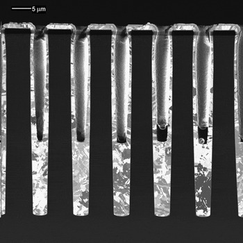
Figure 3 depicts an example from the first application listed (i.e., failure analysis of TSVs). The figure shows a row of 5 × 50 μm TSVs that are partially filled with electrodeposited copper. A 600 × 100 × 50 μm3 volume of silicon was milled from the edge of the sample, with a 1 μA 25 keV Xe+ beam, in a little under one hour. The FIB milled from the underside of the sample to avoid curtaining of the partially filled vias.
Xenon plasma focus ion beam milled cross-section of a row of 5 μm × 50 μm through silicon vias. Sample courtesy of TEL Nexx Inc.

Status and prospects for ICP ion source performance
ICP ion sources are proving to be beneficial for oxygen beam SIMS and large volume FIB milling. However, there is still a great deal of scope for increasing the source brightness and lowering the axial energy spread of this type of ion source, with the prospect of achieving <10 nm spot sizes at 30 keV and 1 pA.
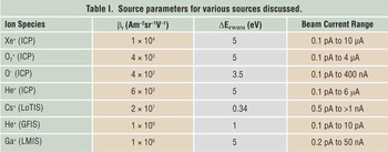
Table I shows the reduced brightness and energy spread for common ion beam species used today. Reference Forbes, Mair and Orloff1–Reference Smith, Tesch, Martin and Boswell3,Reference Hill, Notte and Ward9,Reference Knuffman, Steele and McClelland10 The critical plasma parameters that determine the source brightness are the plasma density and the thermal ion energy distribution, according to Equation 1, where n i is the plasma ion density and E⊥ is the mean thermal ion energy.
 $${\rm{\beta }}_r \propto {\raise0.7ex\hbox{${n_i }$} \!\mathord{\left/ {\vphantom {{n_i } {{\rm{E}}_ \bot }}}\right.\kern-\nulldelimiterspace}\!\lower0.7ex\hbox{${{\rm{E}}_ \bot }$}}$$
Source parameters for various sources discussed.

ICP, inductively coupled plasma; LoTIS, low-temperature ion source; GFIS, gas field ionization source. Reference Forbes, Mair and Orloff1-Reference Smith, Tesch, Martin and Boswell3,Reference Hill, Notte and Ward9,Reference Knuffman, Steele and McClelland10
Hence, the challenge is to maximize n i while minimizing the heating of plasma ions. Today, ICPs are achieving xenon plasma densities of up to 1 × 1013 cm–3 and mean thermal ion energies of ≈0.05 eV, but it is clear that this is not the upper limit to the attainable performance. Pulsed power experiments have shown that the density can be increased by a factor of 10, and continuous power operation is now being pursued. However, it remains to be seen if E⊥ will begin to increase at higher plasma densities, due to phenomena such as RF heating, electron collision heating, and scattering in the plasma sheath.
Currently, the energy spread for positive ion extraction is nominally 5 eV currently for most ion species. Reference Forbes, Mair and Orloff1,Reference Smith, Tesch, Martin and Kinion2 This net energy distribution is due to ions being created at various locations along a field gradient within the plasma (i.e., the plasma pre-sheath), coupled with a temporal modulation of the of the plasma potential that is synchronous with the RF waveform. By sampling the ion energy spread at a fixed RF phase angle, the temporal modulation can be eliminated from the measured energy spread. Using this measurement method, it has been determined at Oregon Physics that temporal modulations are contributing at least 2 eV to the net 5 eV energy distribution. If this temporal modulation of the plasma potential can be eliminated, an energy spread of less than 3 eV is expected.
Advancements in ICP performance will continue to be seen in the coming years, with the possibility of achieving <10 nm beam diameters with oxygen, helium, and xenon ions. Today, if a FIB milling experiment can tolerate a spot size greater than 400 nm, then the ICP Xe+ FIB can provide greater milling speeds than the LMIS Ga+ FIB. However, if the Xe+ ICP brightness could be increased to 2 × 10⁵ Am–2sr–1V–1 and the energy spread reduced to 2.5 eV, then this source will provide FIB milling speed versus resolution that is equivalent to the Ga+ FIB at beam currents less than 6 nA, but also be able to provide several microamp beams focused into a sub-micrometer spot.
Gas field ionization source
Theory of operation
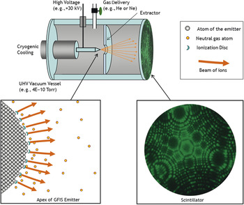
The underlying principle of the gas field ionization source (GFIS) is simple: a sufficiently large electric field can rip an electron from a neutral gas atom, leaving it as a positive ion. This process, field ionization, is explained quantum mechanically as the tunneling of an electron out of a neutral atom under the influence of a large electric field. Reference Muller and Tsong11 For the helium atom, the ionization probability becomes appreciable when the electric field strength approaches 44 V/nm. Reference Muller and Tsong11 Such extremely large electric fields can be attained near the apex of a pointed needle that has been biased positively relative to a nearby extraction electrode. If the needle is sufficiently sharp (100 nm radius of curvature), then only a modest voltage (+20 kV) is needed to create the required electric field. When a small quantity of gas is admitted to this region, the field ionization process can proceed, and ions are created at a typical rate of about 108 s–1. Each newly created ion finds itself in a very strong electric field and is quickly accelerated away from the needle and toward the extractor electrode. For the purpose of visualization, the emission pattern can be observed by introducing a scintillator after the extraction ( Figure 4 ).
The gas field ion source produces an ion emission pattern that corresponds to the atomic arrangement at the apex of the emitter. Under the proper conditions, each of the most protruding atoms generates a steady beam of helium ions. GFIS, gas field ionization source. Reference Muller and Tsong11

Commercialization
As simple as this concept seems, GFIS was not commercialized as an ion source until 2005, 50 years after its first experimental observation. Reference Economou, Notte and Thompson12,Reference Melmed13 Some key advances included control of the emitter shape and precise control of the applied voltage so that only a very small volume experiences the necessary electric field strength. Under the right conditions, the necessary electric field exists solely in disc shaped volumes above the most protruding three atoms (the “trimer”) on the emitter. These ionization discs are estimated to be just a few cubic angstroms in volume, yet produce ions at a rate of about 108 per second—a combination that is critical to producing a beam of high brightness. The small ionization volume also means that all the ions are created at nearly the same electrostatic potential, thereby producing a beam with a narrow energy distribution. Other key enabling features are the ability to maintain atomic arrangement of the emitter for the long periods of time needed for a stable ion beam. These requirements are achieved by a combination of cryogenic cooling, ultrahigh vacuum, and ultrahigh gas purity.
Performance characteristics
The characteristics of the gas field ion source are well suited to produce extremely small focused probe sizes. The reduced brightness is measured to be about 109Am–2sr–1V–1, with a 30 kV extraction voltage. Reference Hill, Notte and Ward9 This remarkably high value is attributed mostly to the very small region from which the ions are produced. We estimate the energy spread of the GFIS beam to be about 1 eV full width at half maximum, small enough to limit the potential issues of chromatic aberration. And like most ion beams, the diffraction effects contribute only a small amount to the overall focused probe size. For these reasons, a relatively simple column consisting of two electrostatic lenses and deflectors allows the GFIS to produce a focused probe size as small as 0.35 nm for helium and 1.9 nm for neon. Reference Hill, Notte, Scipioni and Hawkes14 Such a small beam is well suited to high resolution imaging and fabrication at the nanometer scale. The total emitted current however is limited; the total emission current from the trimer is typically just 100 pA, and only a small portion of one emission site is selected with an aperture, typically allowing less than 5 pA to reach the sample. To achieve the highest resolution cited previously, the probe current must be limited to 0.5 pA or less. Reference Hill, Notte, Scipioni and Hawkes14
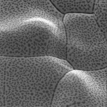
Clearly, this technology is not suited to milling tasks requiring high removal rates; it is better suited to applications where the smallest probe size is required such as imaging and nanofabrication. The available species for the GFIS technique ion beam is somewhat limited. At present, helium is well established for imaging samples with high contrast and surface specificity, as shown in Figure 5 . The contrast here is a combination of topographic contrast and the varying chemical composition of the surface. A new instrument with additional neon capability is also available and affords high sputter rates for nanofabrication. Reference Notte15 Other gas species, however, are not well suited to the GFIS technology because they compromise the emission stability through either chemical attack or condensation at the required cryogenic temperatures.
Chemical vapor deposited nickel after annealing, as imaged with the helium ion microscope using gas field ion source technology. The mottled appearance of the surface likely arises from the rejection of solute during the annealing stage. Sample courtesy of Fibics, Incorporated, Ottawa, Canada.

Low temperature ion source
Theory of operation
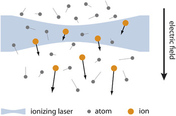
Recently, a new ion source has been developed that generates a Cs+ beam by the photoionization of laser-cooled Reference Metcalf and van der Straten16 gaseous cesium. This is referred to herein as a low-temperature ion source (LoTIS). The development of LoTIS is built upon other conceptually similar systems that employed laser-cooling. Reference Knuffman, Steele, Orloff and McClelland17,Reference Debernardi, Reijnders, Engelen, Clevis, Mutsaers, Luiten and Vredenbregt18 In a LoTIS, gaseous atoms are photoionized by photons from one or more laser beams and then accelerated by an applied electric field to form an ion beam. A schematic of the basic LoTIS concept is shown in Figure 6 . Reference Steele, Knuffman and McClelland19 Once a beam is formed, electrostatic deflectors and lenses may be used to focus it onto a target in a similar fashion to any other FIB system. In this section, the requirements for achieving high performance will be reviewed.
In a low-temperature ion source, gaseous atoms are photoionized from a cold, dense atomic ensemble prepared through the techniques of laser-cooling. Reference Steele, Knuffman and McClelland19

Unlike ICP and GFIS, LoTIS-based systems have yet to be deployed to end-users as part of a complete FIB tool. Therefore, an evaluation of their potential has relied on measurements performed on the ion source itself; knowledge of LoTIS (normalized) brightness and chromatic energy spread enables projections of anticipated focal spot sizes at any given current and beam energy.
The fundamental equation for brightness in a LoTIS is20
 $${\rm{B}} = {J \over {{\rm{\pi }}k_{\rm{B}} T}},$$
where J is the cross-sectional current density of the ion beam generated by the source, k B is Boltzmann’s constant, and T is the temperature of the ions along the directions transverse to the beam. It is helpful to consider the simplest implementation of such a system to get a sense of the values for J and T required to achieve source brightness significantly larger than that of the LMIS value of 106 Am–2sr–1V–1. The current density J is determined by the density of neutral atoms and the efficiency of the laser in ionizing them.
Consider a simplified system where atoms at a given pressure are ionized if they pass through a thin sheet of laser light. A simple estimate of J in this case can be written as Reference Reif21
 $$J = {{\sqrt 2 eP} \over {\sqrt {{\rm{\pi }}mk_{\rm{B}} T} }},$$
where P is the pressure of the gas, and m is the atomic mass. For a pressure of 7 × 10⁻⁴ Pa (5 × 10⁻⁶ Torr) at room temperature, this implies a brightness of less than 40 Am–2sr–1V–1, many orders worse than the LMIS. High brightness operation therefore requires either a large increase in current density or a large reduction in temperature. Laser cooling enables a dramatic reduction in the temperature required to achieve high brightness. The key idea that enables this is that if the photoionization lasers are properly tuned near the threshold for ionization, then the velocity distribution of the ions they create will be nearly identical to that of the neutral atoms.
In the Cs+ LoTIS, atoms are first captured from a low pressure background vapor and formed into a high-flux atomic beam and then compressed using magneto-optical trapping. The beam is cooled using optical molasses Reference Notte15 and then finally photoionized. In one of its simplest forms, an optical molasses is comprised of a pair of oppositely oriented, overlapping laser beams; one pair for each dimension to be cooled. The beams are tuned to a frequency slightly lower than an atomic resonance. An optical molasses creates a viscous-like, velocity-dependent force that brings the atoms to near rest. These atomic collection, compression, and cooling techniques allow for the creation of a cold, dense (above 1017 m–3) atomic ensemble while maintaining background pressures below 10–6 Pa (10–8 Torr) in the part of the source where ions are created. Recently, a system was demonstrated Reference Knuffman, Steele and McClelland10 with J = 0.16 Am–2 and T = 30 µK, giving rise to a Cs+ source with a brightness greater than107 Am–2sr–1V–1.
Not all atomic species are usable with LoTIS because not all are amenable to laser cooling; the alkalis may all be cooled, as may the noble gases and several other metals such as chromium and erbium. Reference Metcalf and van der Straten16 Reductions in temperature to below 100 µK are achievable with a few of these atomic species. However, switching between atoms in the same system presents significant challenges, since each atom requires its own set of lasers for cooling and photoionization. Additionally, densities and temperatures achievable vary greatly between elements, so it is not presently clear which of these species (besides cesium) may be used to create a LoTIS with a brightness larger than that of the LMIS.
The effects of Coulomb interactions are an important consideration in a LoTIS; these interactions will broaden the ion velocity distributions along the directions transverse to the beam, leading to an effective increase in temperature. Because LoTIS has a lower current density at its origin than point emitters such as the LMIS or GFIS, maintaining a low temperature is vital to maintaining high brightness. It was shown, however, Reference Knuffman, Steele and McClelland10,Reference Steele, Knuffman and McClelland19,Reference van der Geer, Reijnders, deLoos, Vredenbregt, Mutsaers and Luiten22 that with a high electric field (105 Vm–1 or greater), by quickly accelerating the ions away from the source as they are created, the heating will be small enough so as to not substantially impact performance, especially in the lower current modes of operation.
The LoTIS has a smaller energy spread than most other ion sources, and this contributes to enhanced performance, especially at lower beam energies and beam currents. As in other FIB systems employing electrostatic lenses, chromatic aberrations must be minimized in order to achieve an optimal focal spot size; these aberrations are proportional to the spread in energies in the ion beam. In a LoTIS, the energy spread is equal to the electric field used to accelerate the ions multiplied by the physical extent of the source along the direction of the field. This size is determined by the size of the ionizing laser(s), typically focused to a couple microns. With an electric field of order 105 Vm–1, this implies an energy spread of a few tenths of an eV, substantially better than the LMIS and similar to the GFIS.
LoTIS developments to date
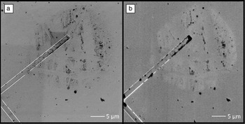
LoTIS-based systems have not been deployed in commercial devices yet. Previous ion source technology that also employed laser-cooling has been incorporated into focused beam prototypes of lithium Reference Knuffman, Steele, Orloff and McClelland17 and chromium. Reference Steele, Knuffman, McClelland and Orloff23 Lithium was selected for an initial test platform because its light mass and high backscatter probability make it well suited to FIB imaging applications. The lithium system fully integrates a laser-cooling-based ion source with a commercial FIB platform from which the LMIS was removed. These test systems demonstrate the feasibility of LoTIS/FIB integration. Additionally, early test systems have shown unique capabilities that will be delivered through the use of new primary ion beams; Figure 7 illustrates the differing image contrast observed in the lithium system when compared with an SEM. Although the overall image resolution is lower than the 1 kV SEM image shown in Figure 7a, the 2 kV Li+ image (Figure 7b) provides complementary imaging mechanisms, including both topographic and material contrast.
Secondary electron images of a contaminated silicon sample (a) using a primary 1 kV electron beam and (b) using a primary beam of 2 kV Li+ ions from low-temperature ion source (LoTIS) focused ion beam technology. Reference Knuffman, Steele, Orloff and McClelland17

The most recent LoTIS development work Reference Knuffman, Steele and McClelland10 shows that these sources can produce Cs+ beams with a brightness greater than 107 Am–2sr–1V–1 and with an energy spread below 0.4 eV. One reason cesium was chosen for this work is that it is the heaviest of the easily laser-coolable atomic species. When fully integrated into an FIB tool, such a system would have numerous advantages. Sub-nm focal spots at 1 pA beam current with a heavy ion would enable nanomachining processes on the finest scales combined with even finer milling and imaging than would occur with a lighter ion. The system’s low energy spread means it should offer enhanced performance at lower accelerating voltages, when compared with other ion sources, as illustrated by the excellent imaging performance at 2 kV shown in Figure 7b. It should offer great flexibility as well. With the capability to output beams with a current of several nA, albeit at reduced brightness, the Cs+ LoTIS will be able to address both fine and medium-scale milling tasks. Additionally, the use of cesium suggests the possibility for development of a tool that can perform secondary ion mass spectrometry tasks as well. The potential of LoTIS-based FIBs may be realized subsequent to further development.
Summary
The ion source technologies presented here extend the capabilities of the conventional gallium LMIS in one aspect or another. These improvements include higher brightness, lower energy spread, and the ability to operate with alternative ion species—or some combination of these. The capabilities of, and applications for, these new technologies are still being explored. In particular, the nest step for LoTIS will include integration with a FIB column and demonstration of its anticipated high performance milling. For GFIS, improvements to the available beam current and alternative ion species are under investigation. When employed in an FIB system, these new ion sources can extend its usefulness to new applications or improve upon the performance of the more well-established ones. These advantages, relative to the gallium LMIS, are anticipated to bring about their commercial acceptance in specific applications.
Acknowledgments
The authors would like to acknowledge Brenton Knuffman and Jabez McClelland for helpful discussions regarding development of the low-temperature ion source.
Disclaimer
Commercial materials identified in this article are not intended to imply recommendation or endorsement by the National Institute of Standards and Technology, nor is it intended to imply that the materials identified are necessarily the best available for the purpose.