Introduction
Two-dimensional (2D) materials, including graphene, Reference Hashimoto, Suenaga, Gloter, Urita and Iijima1–Reference Xia, Mueller, Lin, Valdes-Garcia and Avouris4 hexagonal boron nitride (h-BN), Reference Jin, Lin, Suenaga and Iijima5,Reference Kotakoski, Jin, Lehtinen, Suenaga and Krasheninnikov6 phosphorene, Reference Vierima, Krasheninnikov and Komsa7–Reference Li, Yu, Ye, Ge, Ou, Wu, Feng, Chen and Zhang9 and transition-metal dichalcogenides (TMDCs) Reference Zhou, Zou, Najmaei, Liu, Shi, Kong, Lou, Ajayan, Yakobson and Idrobo10–Reference Radisavljevic, Radenovic, Brivio, Giacometti and Kis12 have been among the most extensively studied materials due to their attractive mechanical, optical, electronic, and chemical properties. Understanding the structure–property relationships in these atomically thin 2D materials requires characterization techniques with atomic resolution and single-atom sensitivity. Aberration-corrected transmission electron microscopy is well suited for such studies. With advances in electron optics and aberration-correction techniques, both conventional transmission electron microscopy (TEM) and scanning TEM (STEM) under low accelerating voltage can now achieve structural analysis at the single-atom level. Reference Krivanek, Chisholm, Nicolosi, Pennycook, Corbin, Dellby, Murfitt, Own, Szilagyi, Oxley, Pantelides and Pennycook13–Reference Suenaga, Wakabayashi, Koshino, Sato, Urita and Iijima17
Even at low voltages, the energy transferred from the e-beam to 2D materials can be high enough to generate local structural distortions or atomic defects Reference Krasheninnikov and Nordlund18,Reference Banhart, Kotakoski and Krasheninnikov19 through knock-on damage associated with the ballistic energy transfer from the impinging electron to the recoil atom, electronic excitations, or beam-induced chemical etching. The key challenge is to control the formation and evolution of structural defects during atomic-resolution (S)TEM experiments. Reference Jin, Lin, Suenaga and Iijima5,Reference Krasheninnikov and Nordlund18,Reference Alem, Erni, Kisielowski, Rossell, Hartel, Jiang, Gannett and Zettl20,Reference Algara-Siller, Kurasch, Sedighi, Lehtinen and Kaiser21 Notably, structural defects considerably impact material properties and can greatly diversify the physical phenomena in 2D materials. While some defects can deteriorate the mechanical and electronic properties, Reference Najmaei, Amani, Chin, Liu, Birdwell, O’Regan, Ajayan, Dubey and Lou22 some are known to introduce enhanced catalytic and magnetic characteristics. Reference Hong, Hu, Probert, Li, Lv, Yang, Gu, Mao, Feng, Xie, Zhang, Wu, Zhang, Jin, Ji, Zhang, Yuan and Zhang11,Reference Li, Tsai, Koh, Cai, Contryman, Fragapane, Zhao, Han, Manoharan, Abild-Pedersen, Norskov and Zheng23 Controlling the formation and distribution of specific types of defects using an e-beam with atomic precision provides a powerful approach for structural modification in 2D materials and tuning of properties.
This article illustrates how engineering 2D materials using an e-beam with atomic precision, while being challenging, is feasible and promising. The formation of structural defects, ranging from zero-dimensional point defects to 2D domains, under e-beam irradiation is discussed. Specifically, point defects can be introduced when the energy transferred from the e-beam to the target atom is higher than the knock-on displacement threshold. Reference Borner, Kaiser and Lehtinen3,Reference Komsa, Kotakoski, Kurasch, Lehtinen, Kaiser and Krasheninnikov24–Reference Lehnert, Lehtinen, Algara-Siller and Kaiser26 Further e-beam bombardment can induce migration or reconstruction of the atomic network at point defects if the imparted energy is comparable to the atom binding energy. Reference Kotakoski, Eder and Meyer27,Reference Komsa, Kurasch, Lehtinen, Kaiser and Krasheninnikov28 Such migration of point defects can be viewed as letting the system explore thermodynamically (meta)stable states in selected regions under energy supplied from the e-beam. It is shown that anion vacancies in TMDC monolayers tend to agglomerate and form one-dimensional (1D) defects Reference Komsa, Kurasch, Lehtinen, Kaiser and Krasheninnikov28,Reference Lin, Pantelides and Zhou29 (e.g., line defects and grain boundaries), which are expected to have a substantial impact on the electronic transport properties. Reference Li, Long, Cui, Yang, Zhang, Ding and Xu30,Reference Zhang, Zou, Crespi and Yakobson31 By manipulating the formation and evolution of defects via e-beam irradiation, the defect landscape in 2D materials can be controlled.
We also illustrate that extensive e-beam irradiation can trigger phase transformation in 2D materials, especially when combined with in situ heating. Reference Sutter, Huang, Komsa, Ghorbani-Asl, Krasheninnikov and Sutter32 In addition, novel nanostructures, which might not be grown by conventional methods, can be controllably fabricated under e-beam irradiation. Examples include the selective sculpting of 1D atomic chains Reference Xiao, Qiao, Lu, Ye, Chen, Zhang, Ji, Li and Jin8,Reference Chuvilin, Meyer, Algara-Siller and Kaiser33–Reference Cretu, Komsa, Lehtinen, Algara-Siller, Kaiser, Suenaga and Krasheninnikov36 and subnanometer nanowires Reference Liu, Xu, Wu, Zhang, Yu, Qiu, Hong, Jin, Li, Wang, Sun and Guo37–Reference Koh, Wang, Ataca, Grossman, Sinclair and Warner41 in a monolayer matrix using a focused e-beam and the formation of new atomically thin 2D materials (monolayer Fe Reference Zhao, Deng, Bachmatiuk, Sandeep, Popov, Eckert and Rümmeli42 and monolayer copper oxide Reference Yin, Zhang, Zhou, Sun, Chisholm, Pantelides and Zhou43,Reference Kano, Kvashnin, Sakai, Chernozatonskii, Sorokin, Hashimoto and Takeguchi44 ) via self-assembly of adatoms on a graphene surface (or in graphene nanopores) under e-beam irradiation.
Atomic-point defects in 2D materials
The formation of intrinsic-point defects in 2D materials is inevitable as dictated by the laws of thermodynamics. Reference Banhart, Kotakoski and Krasheninnikov19 The atomic structure of point defects has been widely investigated in graphene using electron microscopy imaging, Reference Hashimoto, Suenaga, Gloter, Urita and Iijima1 and several typical point defects, including the Stone–Wales defect in graphene, Reference Meyer, Kisielowski, Erni, Rossell, Crommie and Zettl2,Reference Suenaga, Wakabayashi, Koshino, Sato, Urita and Iijima17 single vacancies (SVs), Reference Meyer, Kisielowski, Erni, Rossell, Crommie and Zettl2 double vacancies (DVs), Reference Algara-Siller, Kurasch, Sedighi, Lehtinen and Kaiser21 and dislocation cores Reference Lehtinen, Kurasch, Krasheninnikov and Kaiser14,Reference Warner, Margine, Mukai, Robertson, Giustino and Kirkland16 have been successfully imaged and identified. In monolayer h-BN, where electron-induced damage is hard to avoid during atomic-resolution imaging, the lower knock-on displacement threshold of B, as compared to N atoms, Reference Jin, Lin, Suenaga and Iijima5,Reference Kotakoski, Jin, Lehtinen, Suenaga and Krasheninnikov6 has led to boron vacancies (VB) being the dominant point defects observed in this material, and triangular holes formed in h-BN are predominantly terminated by nitrogen. Reference Jin, Lin, Suenaga and Iijima5,Reference Meyer, Chuvilin, Algara-Siller, Biskupek and Kaiser45,Reference Pham, Gibb, Li, Gilbert, Song, Louie and Zett46
In the case of monolayer MoS2, a representative three-atom-thick semiconducting TMDC material, a rich variety of point defect structures, was observed. Reference Zhou, Zou, Najmaei, Liu, Shi, Kong, Lou, Ajayan, Yakobson and Idrobo10 Six different types of prevailing point defects were identified in monolayer MoS2, namely ( Figure 1a) a monosulfur vacancy (VS), (Figure 1b) a disulfur vacancy (VS2), (Figure 1c) an antisite defect in which a Mo atom substitutes a S2 column (MoS2), (Figure 1d) a vacancy complex of Mo with three nearby sulfur atoms (VMoS3), (Figure 1e) a vacancy complex of Mo with three nearby disulfur pairs (VMoS6), and (Figure 1f) an antisite defect in which a S2 column replaces a Mo atom (S2Mo). Reference Zhou, Zou, Najmaei, Liu, Shi, Kong, Lou, Ajayan, Yakobson and Idrobo10,Reference Komsa and Krasheninnikov25 Various adatoms and interstitial atoms in chemical vapor deposition (CVD) grown monolayer MoS2 have also been observed using low-voltage STEM annular dark-field (ADF) imaging. Reference Zhou, Zou, Najmaei, Liu, Shi, Kong, Lou, Ajayan, Yakobson and Idrobo10
Point defects in 2D materials. (a–f) Scanning transmission electron microscope annular dark-field images of VS, VS2, MoS2, VMoS3, VMoS6, and S2Mo type of point defects in a MoS2 monolayer, respectively. Reference Zhou, Zou, Najmaei, Liu, Shi, Kong, Lou, Ajayan, Yakobson and Idrobo10 Scale bars are 0.5 nm. (g) Formation energies of different point defects in a MoS2 monolayer as a function of the chemical potential of sulfur (μS). Reference Komsa and Krasheninnikov25 (h) Histograms of the densities of various point defects in MoS2 monolayers prepared by physical vapor deposition (PVD), chemical vapor deposition (CVD), and mechanical exfoliation (ME). Reprinted with permission from Reference Hong, Hu, Probert, Li, Lv, Yang, Gu, Mao, Feng, Xie, Zhang, Wu, Zhang, Jin, Ji, Zhang, Yuan and ZhangReference 11. © 2015 Macmillan Publishers Ltd.

The diverse atomic arrangements endow each type of atomic-point defect with different electronic structure and functionality. The most common point defects in CVD grown MoS2 are sulfur vacancies (VS and VS2), Reference Zhou, Zou, Najmaei, Liu, Shi, Kong, Lou, Ajayan, Yakobson and Idrobo10 which are believed to be responsible for the n-type conductivity Reference Zhou, Zou, Najmaei, Liu, Shi, Kong, Lou, Ajayan, Yakobson and Idrobo10,Reference Komsa and Krasheninnikov25 observed in this material. Theoretical calculations reveal that antisite defects (Mo replacing a S atom) have a local magnetic moment. Reference Hong, Hu, Probert, Li, Lv, Yang, Gu, Mao, Feng, Xie, Zhang, Wu, Zhang, Jin, Ji, Zhang, Yuan and Zhang11 Therefore, controlling the relative population of various point defects in MoS2, either during growth or via e-beam irradiation, serves as an effective way to tune the properties of this material.
Density functional theory (DFT) calculations Reference Zhou, Zou, Najmaei, Liu, Shi, Kong, Lou, Ajayan, Yakobson and Idrobo10,Reference Komsa and Krasheninnikov25 show that the formation energy of various point defects in a MoS2 monolayer is highly dependent on the chemical potential of sulfur (Figure 1g). Sulfur vacancies (VS) exhibit the lowest formation energy among all point defects observed experimentally, except for interstitial sulfur atoms (SI) under S-rich conditions, which is consistent with experimental observations. Reference Zhou, Zou, Najmaei, Liu, Shi, Kong, Lou, Ajayan, Yakobson and Idrobo10,Reference Hong, Hu, Probert, Li, Lv, Yang, Gu, Mao, Feng, Xie, Zhang, Wu, Zhang, Jin, Ji, Zhang, Yuan and Zhang11 Another important implication from the DFT results is that a distinct growth environment can change the predominant type of point defects (Figure 1h), and consequently, the intrinsic properties of monolayer MoS2 can be manipulated via growth engineering.
Point defects can also be further introduced via e-beam irradiation. Komsa et al. successfully demonstrated the creation of point defects, predominantly anion vacancies in monolayer MoS2 triggered by e-beam irradiation. Reference Komsa, Kotakoski, Kurasch, Lehtinen, Kaiser and Krasheninnikov24 Although the calculated knock-on damage threshold is 80 kV or higher, Reference Komsa, Kotakoski, Kurasch, Lehtinen, Kaiser and Krasheninnikov24 VS and VSe defects were still generated in monolayer TMDCs under prolonged e-beam irradiation even at a lower voltage of 60 kV. Reference Lin, Pantelides and Zhou29 This is clearly different from graphene, where knock-on damage prevails Reference Borner, Kaiser and Lehtinen3,Reference Meyer, Eder, Kurasch, Skakalova, Kotakoski, Park, Roth, Chuvilin, Eyhusen, Benner, Krasheninnikov and Kaiser47 (i.e., a sputtering event only occurs when the energy transferred from an energetic electron to the target atom is higher than the displacement threshold). The experimental results indicate that defect generation in semiconducting TMDCs monolayers under e-beam irradiation most likely proceeds via ionization damage or is catalyzed by hydrocarbon surface contaminants. Reference Zhou, Zou, Najmaei, Liu, Shi, Kong, Lou, Ajayan, Yakobson and Idrobo10,Reference Lin, Pantelides and Zhou29 Whatever the mechanism of defect production, electron-beam irradiation provides a simple way to generate additional anion vacancies in selected regions in monolayer TMDCs, which can then be driven to form other functional defects (as discussed later).
Structural dynamics of atomic defects under an e-beam
Apart from defect creation via atom sputtering, elastic collisions that transfer energy comparable to the binding energy of the atoms are perhaps even more interesting from the perspective of atomic-level manipulation of materials—they can lead to atom-number-conserving rearrangements that can be stochastically induced by controlling the electron dose and the energy. Such processes have the potential to create specific atomic arrangements within 2D materials, without a net loss of atoms or the formation of holes.
A characteristic example of such a process is the formation and annihilation of the so-called Reference Monthioux and Charlier48 Stone–Wales defect in graphene Reference Meyer, Kisielowski, Erni, Rossell, Crommie and Zettl2,Reference Suenaga, Wakabayashi, Koshino, Sato, Urita and Iijima17 that occurs due to a 90° rotation of one of the C–C bonds, initiated by an electron impact on one of the involved carbon atoms. Reference Kotakoski, Meyer, Kurasch, Santos-Cottin, Kaiser and Krasheninnikov49 Similar bond-rotation-type transformations have also been observed at other graphene defects, such as divacancies, Reference Borner, Kaiser and Lehtinen3,Reference Kotakoski, Mangler and Meyer15,Reference Kotakoski, Krasheninnikov, Kaiser and Meyer50,Reference Robertson, Montanari, He, Allen, Wu, Harrison, Kirkland and Warner51 grain boundaries, Reference Kurasch, Kotakoski, Lehtinen, Skakalova, Smet, Krill, Krasheninnikov and Kaiser52 atomic configurations involving implanted carbon atoms, Reference Lehtinen, Vats, Algara-Siller, Knyrim and Kaiser53 dislocation cores, Reference Lehtinen, Kurasch, Krasheninnikov and Kaiser14,Reference Warner, Margine, Mukai, Robertson, Giustino and Kirkland16 and graphene edges. Reference Gong, He, Robertson, Yoon, Lee and Warner54,Reference He, Robertson, Fan, Allen, Lin, Suenaga, Kirkland and Warner55 This process can also heal graphene defects, or even small grains, such as the so-called “flower defect” that can be formed by rotating six carbon–carbon bonds in sequence. Reference Kurasch, Kotakoski, Lehtinen, Skakalova, Smet, Krill, Krasheninnikov and Kaiser52 E-beam induced bond rotations can also lead to migration of defects through the lattice, as highlighted by the observations of a random walk of a divancy Reference Kotakoski, Mangler and Meyer15 and dislocation glide. Reference Lehtinen, Kurasch, Krasheninnikov and Kaiser14,Reference Warner, Margine, Mukai, Robertson, Giustino and Kirkland16
E-beam induced structural changes that do not involve removal of atoms can also occur at impurity sites. In the case of a Si atom in a threefold configuration embedded within the graphene lattice, this process leads to place-exchange between the Si atom and one of its carbon neighbors (a bond inversion). Reference Susi, Kotakoski, Kepaptsoglou, Mangler, Lovejoy, Krivanek, Zan, Bangert, Ayala, Meyer and Ramasse56 Here, an electron impacts the carbon neighbor and sends it off to a trajectory above the graphene sheet. Due to the attractive interaction with the silicon atom, the displaced carbon atom travels on a curved path toward the Si. However, while the C is above the structure, the Si atom moves into the newly created vacancy. Hence, when the C returns to the lattice, it must take the previous place of the Si atom. Because this process has a strong directional component (Si moves to the location of the impacted C), it can be used to systematically move impurity atoms in the graphene lattice. The possibility for controlled relocation of a Si impurity in graphene based on this mechanism was predicted, Reference Susi, Kotakoski, Kepaptsoglou, Mangler, Lovejoy, Krivanek, Zan, Bangert, Ayala, Meyer and Ramasse56 and recently, controlled displacement over several atomic steps was experimentally demonstrated Reference Susi, Meyer and Kotakoski57 ( Figure 2 ). Other impurity atoms that have shown similar behavior include nitrogen in a pyridinic configuration in graphene (in which the nitrogen atom replaces exactly one carbon atom with one of the neighbors missing) that has been observed to jump repeatedly over its associated vacancy. Reference Lin, Teng, Yeh, Koshino, Chiu and Suenaga58
Scanning transmission electron microscope annular dark-field images showing controlled relocation of a Si impurity in graphene. In each step, the e-beam is parked on the position marked by the white dot, until the Si (appearing in panels with bright contrast within the graphene lattice) and the C atom exchange places (dashed lines show where the impurity has moved further than intended). Scale bar = 0.5 nm. Reference Susi, Meyer and Kotakoski57

In other 2D materials, most observed dynamics involve sputtered atoms. However, heavier adatoms have been observed to migrate on top of MoS2, Reference Lin, Dumcenco, Komsa, Niimi, Krasheninnikov, Huang and Suenaga59 possibly driven by the e-beam. Curiously, even bond-rotation-type events have been observed at least in WSe2, where, combined with vacancies, they lead to the creation of threefold rotational defects. Reference Lin, Bjorkman, Komsa, Teng, Yeh, Huang, Lin, Jadczak, Huang, Chiu, Krasheninnikov and Suenaga60
One-dimensional defects and their dynamics
Upon longer e-beam irradiation with energy transfer comparable to the binding energy of the atoms, atomic defects can migrate over longer distances and agglomerate with other atomic defects. Reference Komsa, Kurasch, Lehtinen, Kaiser and Krasheninnikov28,Reference Lin, Pantelides and Zhou29 Ultimately, 1D defects (e.g., vacancy line defects Reference Wang, Lee, Lee, Yoon and Warner61 or grain boundaries) Reference Lin, Pantelides and Zhou29 evolve in this way from abundant point defects.
Line defects, among the most important extended defects, govern the properties of any crystalline material and have been investigated in many representative 2D systems. The evolution of line defects in graphene was observed Reference Lehtinen, Kurasch, Krasheninnikov and Kaiser14 using impinging energetic electrons both to image and stimulate atomic-scale changes in the material structure. The transformations were followed in situ, atom-by-atom in a TEM, showing the full life cycle of a dislocation from birth to annihilation.
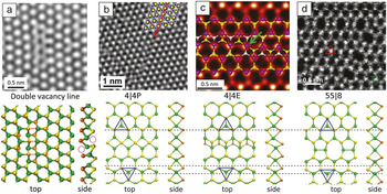
It was revealed that the evolution of dislocations in 2D systems is governed by markedly long-range out-of-plane buckling. Moreover, several in situ TEM experiments Reference Komsa, Kurasch, Lehtinen, Kaiser and Krasheninnikov28,Reference Lin, Pantelides and Zhou29,Reference Lehtinen, Komsa, Pulkin, Whitwick, Chen, Lehnert, Mohn, Yazyev, Kis, Kaiser and Krasheninnikov40,Reference Lin, Bjorkman, Komsa, Teng, Yeh, Huang, Lin, Jadczak, Huang, Chiu, Krasheninnikov and Suenaga60 showed that agglomeration of vacancies in TMDCs gives rise to the formation of line defects and development of grains embedded in larger grains with 60° relative rotation in crystal orientation. An interesting and somewhat unexpected observation was that depending on the chemical content of TMDCs, line defects with different morphologies are formed. For example, agglomeration of vacancies in MoS2 under e-beam gives rise to straight vacancy lines without any substantial local transformations of the atomic structure ( Figure 3a), Reference Komsa, Kurasch, Lehtinen, Kaiser and Krasheninnikov28 while the sputtering of chalcogen atoms in WSe2 or WS2 (Figure 3d) results in rotational defects and mirror grains with the boundaries consisting of five- and eight-member rings. Reference Lin, Bjorkman, Komsa, Teng, Yeh, Huang, Lin, Jadczak, Huang, Chiu, Krasheninnikov and Suenaga60 The appearance of different line structures in MoSe2 was also reported Reference Lin, Pantelides and Zhou29,Reference Lehtinen, Komsa, Pulkin, Whitwick, Chen, Lehnert, Mohn, Yazyev, Kis, Kaiser and Krasheninnikov40 under similar conditions. Reference Komsa and Krasheninnikov62
Examples of line defects in 2D transition-metal dichalcogenides. Top panels show the high-resolution or scanning transmission electron microscope (HRTEM or STEM) images, and the lower panels represent the corresponding atomic structures (Mo/W, green; S/Se, yellow or brown). (a) HRTEM image of monolayer MoS2 with a staggered double vacancy line (top panel) and the corresponding atomic structure (bottom panel). Reference Komsa, Kurasch, Lehtinen, Kaiser and Krasheninnikov28 (b–d) Three types of mirror twin-boundary (MTB) structures. (b) 4|4P MTB in MoSe2 (HRTEM image, Mo is blue in the overlaid structure), Reference Lehtinen, Komsa, Pulkin, Whitwick, Chen, Lehnert, Mohn, Yazyev, Kis, Kaiser and Krasheninnikov40 (c) 4|4E MTB in MoS2 (STEM annular dark-field [ADF] image, overlaid structure shows Mo, purple, and a lower layer of S, white), Reference Zhou, Zou, Najmaei, Liu, Shi, Kong, Lou, Ajayan, Yakobson and Idrobo10 (d) 55|8 MTB in WSe2 (STEM ADF image). Reference Lin, Bjorkman, Komsa, Teng, Yeh, Huang, Lin, Jadczak, Huang, Chiu, Krasheninnikov and Suenaga60 The triangles in the lower panels highlight the registry of the lattice at the two sides of the MTB. The dashed horizontal lines highlight strain in the perpendicular direction when the lattices are aligned at the top.

Grain boundaries are particularly important for understanding the mechanical and electronic properties of polycrystalline 2D materials synthesized by CVD and related techniques. Grain boundaries normally appear during the growth when islands of the emerging material with different crystal orientations coalesce. Depending on the misorientation angle and growth conditions, the morphology of the boundaries can be quite different. For instance, grain boundaries in graphene consist mostly of nonhexagonal rings, including pentagons, heptagons, and octagons, and they can be straight or serpentine Reference Kurasch, Kotakoski, Lehtinen, Skakalova, Smet, Krill, Krasheninnikov and Kaiser52,Reference Huang, Ruiz-Vargas, van der Zande, Whitney, Levendorf, Kevek, Garg, Alden, Hustedt, Zhu, Park, McEuen and Muller63 depending on the misorientation angle between the grains. The evolution of grain boundaries in graphene under e-beam irradiation was followed in situ in a TEM, Reference Kurasch, Kotakoski, Lehtinen, Skakalova, Smet, Krill, Krasheninnikov and Kaiser52 revealing configurational fluctuations that take on a time-averaged preferential direction only in the presence of significant boundary curvature, as confirmed by Monte Carlo simulations. Remarkably, in the extreme case of a small graphene grain enclosed within a larger one, its shrinkage to the point of complete disappearance was observed.
The structure of grain boundaries Reference Zhou, Zou, Najmaei, Liu, Shi, Kong, Lou, Ajayan, Yakobson and Idrobo10,Reference Azizi, Zou, Ercius, Zhang, Elias, Perea-Lopez, Stone, Terrones, Yakobson and Alem64–Reference van der Zande, Huang, Chenet, Berkelbach, You, Lee, Heinz, Reichman, Muller and Hone66 in TMDCs can also vary (Figure 3). While tilt and mirror twin boundaries (MTBs) in MoS2 (Figure 3c) were reported to consist of eight- and/or four-membered rings, Reference Zhou, Zou, Najmaei, Liu, Shi, Kong, Lou, Ajayan, Yakobson and Idrobo10,Reference Lin, Pantelides and Zhou29,Reference van der Zande, Huang, Chenet, Berkelbach, You, Lee, Heinz, Reichman, Muller and Hone66 another study pointed to the existence of five- and seven-membered rings. Reference Najmaei, Liu, Zhou, Zou, Shi, Lei, Yakobson, Idrobo, Ajayan and Lou65 MTBs have been reported in MoSe2 (Figure 3b) because of chalcogen atom deficiency during growth. Reference Lehtinen, Komsa, Pulkin, Whitwick, Chen, Lehnert, Mohn, Yazyev, Kis, Kaiser and Krasheninnikov40 In semiconducting TMDCs, grain boundaries and other 1D defects can be conducting channels, Reference Zhou, Zou, Najmaei, Liu, Shi, Kong, Lou, Ajayan, Yakobson and Idrobo10,Reference Lin, Pantelides and Zhou29,Reference Lehtinen, Komsa, Pulkin, Whitwick, Chen, Lehnert, Mohn, Yazyev, Kis, Kaiser and Krasheninnikov40,Reference Wang, Lee, Lee, Yoon and Warner61,Reference van der Zande, Huang, Chenet, Berkelbach, You, Lee, Heinz, Reichman, Muller and Hone66–Reference Barja, Wickenburg, Liu, Zhang, Ryu, Ugeda, Hussain, Shen, Mo, Wong, Salmeron, Wang, Crommie, Ogletree, Neaton and Weber-Bargioni68 while electronic transport in the direction perpendicular to the boundaries is normally suppressed. First-principles calculations indicate that some line defects in TMDCs exhibit magnetism, Reference Zhang, Zou, Crespi and Yakobson31,Reference Lehtinen, Komsa, Pulkin, Whitwick, Chen, Lehnert, Mohn, Yazyev, Kis, Kaiser and Krasheninnikov40,Reference Le and Rahman67 thus adding new functionalities to the system. Grain boundaries have been demonstrated to exhibit fascinating charge-density wave behavior Reference Barja, Wickenburg, Liu, Zhang, Ryu, Ugeda, Hussain, Shen, Mo, Wong, Salmeron, Wang, Crommie, Ogletree, Neaton and Weber-Bargioni68 as quasi-1D metallic channels embedded in the semiconducting matrix. Controlling the generation and annihilation of 1D defects using an electron beam thus provides new possibilities to tune the functionalities of 2D materials.
Phase transformation under e-beam irradiation
High-energy electrons can induce controlled structural transformations by knock-on collisions that can break bonds, displace atoms, and induce point defects, or by other mechanisms such as local charge buildup. Hence, complete phase transitions of 2D materials can be accomplished via controlled e-beam irradiation.
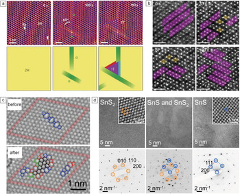
In graphene, electron irradiation near the knock-on threshold was shown to drive the transformation from crystalline to an amorphous 2D membrane of sp Reference Meyer, Kisielowski, Erni, Rossell, Crommie and Zettl2 -hybridized carbon atoms. Reference Kotakoski, Krasheninnikov, Kaiser and Meyer50 Irradiation creates carbon vacancies and provides activation energy to drive the system between local energy minima via reversible-bond rotations. Continued irradiation and C loss produces clusters of 30°-rotated hexagons surrounded by alternating pentagons and heptagons ( Figure 4c), which cancel negative and positive curvature so that the overall structure remains planar. At later stages, real-time imaging and reciprocal-space analysis show a sharp drop in overall crystallinity with defects growing into a vitreous network separating shrinking honeycomb crystallites Reference Eder, Kotakoski, Kaiser and Meyer69 (i.e., a transition from a nanocrystalline structure [similar to 2D silica glass]70 to a final state approaching a random network). A related glassy (“Zachariasen”) Reference Zachariasen71 sp 2 carbon monolayer was synthesized by CVD. Reference Joo, Lee, Jang, Kang, Kwon, Chung, Lee, Kim, Kim, Yang, Kim, Choi, Whang and Hwang72 The transformation of hydrocarbon adsorbates on graphene into amorphous C monolayers followed by crystallization has been imaged at high temperatures, Reference Westenfelder, Meyer, Biskupek, Kurasch, Scholz, Krill and Kaiser73 demonstrating the ability to probe both beam-induced and thermally driven structural transformations at the atomic scale.
Electron-beam-induced transformations of 2D and layered crystals. (a) Scanning transmission electron microscope annular dark-field (STEM ADF) images of reversible conversion between 2H and 1T phases of MoS2 via an intermediate α phase (white arrows indicate Re dopant atoms). Reprinted with permission from Reference Lin, Dumcenco, Huang and SuenagaReference 82. © 2014 Macmillan Publishers Ltd. (b) STEM ADF images of reorientation of W-atom zigzag chains in the distorted 1T phase of WS2 (ZT phase, highlighted in purple; DT phase, highlighted in yellow). Scale bars = 1 nm. Reprinted with permission from Reference Amara, Chen, Lin, Kumar, Okunishi, Suenaga, Quek and EdaReference 83. © 2016 American Chemical Society. (c) High-resolution transmission electron microscope (HRTEM) images showing conversion of crystalline graphene to an amorphous sp 2 carbon membrane. Reference Kotakoski, Krasheninnikov, Kaiser and Meyer50 (d) HRTEM images showing knock-on-induced transformation from few-layer SnS2 to SnS. Reference Sutter, Huang, Komsa, Ghorbani-Asl, Krasheninnikov and Sutter32 Inset shows enlarged images. Corresponding diffraction images are shown in lower panel.

Beyond graphene, monolayer TMDC materials offer new opportunities for driving and imaging phase changes. TMDCs such as MoS2 crystallize in different polymorphs. In addition to the ground-state semiconducting trigonal prismatic (2H) phase with S(A)-Mo(b)-S′(A) stacking, MoS2 can crystallize in higher-energy octahedral 1T (S(A)-Mo(b)-S′(C)) or distorted 1T (ZT—displaying a 2 × 1 superstructure, or DT—a 2 × 2 superstructure) phases, which are metallic. Reference Chhowalla, Shin, Eda, Li, Loh and Zhang74 Conversion between these phases, important for realizing low-resistance contacts for devices Reference Kappera, Voiry, Yalcin, Branch, Gupta, Mohite and Chhowalla75 or in electrocatalysis, Reference Lukowski, Daniel, Meng, Forticaux, Li and Jin76,Reference Wang, Lu, Kong, Sun, Hymel and Cui77 can be achieved by electron donation (e.g., via alkali metal intercalation Reference Py and Haering78–Reference Xiong, Wang, Liu, Sun, Brongersma, Pop and Cui80 or doping Reference Kappera, Voiry, Yalcin, Branch, Gupta, Mohite and Chhowalla75,Reference Enyashin, Yadgarov, Houben, Popov, Weidenbach, Tenne, Bar-Sadan and Seifert81 ). Electron-beam irradiation in STEM accumulates sufficient charge to trigger the transformation, and can thus probe the atomistic steps that accompany the S-plane gliding in the 2H to 1T transition. Reference Wang, Xu, Wang and Bai79,Reference Lin, Dumcenco, Huang and Suenaga82 In situ STEM observations at high temperatures show in detail the processes that ultimately lead to the lattice-plane glide underlying the transformation (Figure 4a). The process is initiated by the creation of narrow bands of a α-phase precursor in the starting (2H) phase. Strain buildup between emerging α-phase bands triggers an S′-plane (or Mo-S) glide to form a triangular nucleus of the new (1T) phase, which further expands via secondary (β, γ) boundary structures into the 2H MoS2 host crystal.
E-beam irradiation also affects the distorted 1T structure of MoS2 (and WS2). Reference Amara, Chen, Lin, Kumar, Okunishi, Suenaga, Quek and Eda83 Charge buildup during STEM imaging, which weakens the metal–chalcogen bond, causes reorientation of the metal-atom zigzag chains via the local formation of tetramer clusters (Figure 4b), adding to the growing library of approaches for 2D TMDC phase engineering.
While some TMDCs have multiple competing phases with the same composition, other 2D or layered chalcogenides can access stable phases with different stoichiometry. Tin-based materials can exist as dichalcogenides (e.g., SnS2), “2–3” compounds (Sn2S3), and monochalcogenides (SnS) with different lattice structures, Reference Gomes and Carvalho84 as well as optoelectronic Reference Sutter, Huang, Komsa, Ghorbani-Asl, Krasheninnikov and Sutter32,Reference George and Joseph85,Reference Huang, Sutter, Sadowski, Cotlet, Monti, Racke, Neupane, Wickramaratne, Lake, Parkinson and Sutter86 and device properties. Reference Huang, Sutter, Sadowski, Cotlet, Monti, Racke, Neupane, Wickramaratne, Lake, Parkinson and Sutter86–Reference Zhao, Lo, Zhang, Sun, Tan, Uher, Wolverton, Dravid and Kanatzidis90 Knock-on collisions during electron irradiation primarily affect the chalcogen atoms (i.e., generate S [Se] vacancies and can ultimately transform dichalcogenides into monochalcogenides), Reference Sutter, Huang, Komsa, Ghorbani-Asl, Krasheninnikov and Sutter32 either as nanoscale domains or uniformly across large areas at elevated temperatures (200–400°C). Few-layer SnS2 transforms into tilted (21° off-axis) SnS (Figure 4d). Calculations explain this by a pathway involving the formation of S-vacancy lines followed by rotational realignment of the intervening crystal segments to a local Sn2S3 structure that defines the tilt of the final SnS phase. For ultrathin SnS2, this pathway is geometrically inaccessible and the product is basal-plane-oriented SnS. This effect can be used to select chemically inert or reactive (open-edge) configurations of SnS.
An emerging possibility in transforming layered materials is the conversion to a structure having different dimensionality (e.g., from a 2D to a 1D system). The Sn2S3 intermediate in the SnS2 to SnS transformation, for example, would comprise bundles of narrow SnS2 nanowires if realized over large areas (up to several hundred nanometers). Reference Sutter, Huang, Komsa, Ghorbani-Asl, Krasheninnikov and Sutter32 For 2H-MoTe2, thermally activated Te desorption at elevated temperatures (400–500°C) drives local conversion to an array of 1D Mo6Te6 nanowires, Reference Zhu, Wang, Zhang, Addou, Cho, Wallace and Kim91 crystallographically aligned with the few-layer 2H-MoTe2 host and predicted to be metallic. Such sub-nm metallic MX (M = Mo or W, X = S or Se) nanowires can also be produced individually in the 2D TMDCs matrix using e-beam sculpting.
Creating new nanostructures under an e-beam
One of the advantages of using the electron beam in STEM to modify the atomic structure of the material is that the irradiation region can be controlled with high precision. In particular, in aberration-corrected STEM, a focused e-beam with sub-angstrom size can be precisely controlled to interact locally with specific target atoms (as demonstrated in Figure 2), so that sculpting novel nanostructures with atomic precision becomes possible. For example, 1D atomic chains and three-atom-wide nanowires can be created in situ within 2D monolayers. Reference Chuvilin, Meyer, Algara-Siller and Kaiser33,Reference Jin, Lan, Peng, Suenaga and Iijima34,Reference Cretu, Komsa, Lehtinen, Algara-Siller, Kaiser, Suenaga and Krasheninnikov36–Reference Lin, Cretu, Zhou, Suenaga, Prasai, Bolotin, Cuong, Otani, Okada, Lupini, Idrobo, Caudel, Burger, Ghimire, Yan, Mandrus, Pennycook and Pantelides38,Reference Lehtinen, Komsa, Pulkin, Whitwick, Chen, Lehnert, Mohn, Yazyev, Kis, Kaiser and Krasheninnikov40 In addition, when the right amount of energy is imparted from the e-beam to drive the system between local energy minima, metastable structures that cannot be obtained via conventional synthesis may be accessed and explored. New 2D materials, such as monolayer Fe Reference Zhao, Deng, Bachmatiuk, Sandeep, Popov, Eckert and Rümmeli42 and one-atom-thick copper oxide monolayers, Reference Yin, Zhang, Zhou, Sun, Chisholm, Pantelides and Zhou43,Reference Kano, Kvashnin, Sakai, Chernozatonskii, Sorokin, Hashimoto and Takeguchi44 have been created and discovered in STEM.
Atomic chains were first created in graphene via e-beam sputtering of carbon atoms. Reference Chuvilin, Meyer, Algara-Siller and Kaiser33,Reference Jin, Lan, Peng, Suenaga and Iijima34 Atomic carbon chains have been experimentally proven to be conductive, although the conductivity proved to be lower than the calculated values for unstrained chains. Reference Cretu, Botello-Mendez, Janowska, Cuong, Charlier and Banhart92 The carbon atoms in such 1D atomic chains can take on two distinct arrangements, namely cumulene with identical-length double bonds or polyyne with alternating single and triple bonds ( Figure 5a). The different arrangements are reflected in varied C–C bond length, and a recent study finds an unexpectedly high dimerization ratio in such 1D carbon atomic chains (i.e., the polyyne structure) created under the e-beam at elevated temperatures. Reference Lin, Morishita, Koshino, Yeh, Teng, Chiu, Sawada and Suenaga35 One-dimensional atomic chains with alternating B–N–B–N arrangement have also been produced in h-BN under e-beam (Figure 5b), and they remain insulating as suggested by theory. Reference Cretu, Komsa, Lehtinen, Algara-Siller, Kaiser, Suenaga and Krasheninnikov36 The stability of heteroatomic chains is significantly enhanced once they are supported by an h-BN layer. Atomic chains of phosphorene (Figure 5c), a promising direct-bandgap semiconductor, have been predicted to be ultrastable and (semi-)metallic due to the unique noncollinear zigzag configuration of phosphorus atoms. Reference Vierima, Krasheninnikov and Komsa7 Xiao et al. recently fabricated P atomic chains in phosphorene, and the formation, migration, and breakage of the atomic chains were directly captured by TEM imaging. Reference Xiao, Qiao, Lu, Ye, Chen, Zhang, Ji, Li and Jin8
Novel nanostructures created in 2D materials under electron irradiation. (a–c) Atomic chains derived from (a) graphene via scanning transmission electron microscopy (STEM), (b) hexagonal boron nitride, Reference Cretu, Komsa, Lehtinen, Algara-Siller, Kaiser, Suenaga and Krasheninnikov36 and (c) phosphorene via high-resolution transmission electron microscope (ac, armchair direction). (a) Reprinted with permission from Reference Lin, Morishita, Koshino, Yeh, Teng, Chiu, Sawada and SuenagaReference 35. © 2017 American Chemical Society. (c) Reprinted with permission from Reference Xiao, Qiao, Lu, Ye, Chen, Zhang, Ji, Li and JinReference 8. © 2017 Springer. (d) Patterning of MoSe nanowires in a MoSe2 monolayer. Reference Lin, Cretu, Zhou, Suenaga, Prasai, Bolotin, Cuong, Otani, Okada, Lupini, Idrobo, Caudel, Burger, Ghimire, Yan, Mandrus, Pennycook and Pantelides38 STEM annular dark field (STEM ADF) images of individual MoS, MoSe, and WSe nanowires, respectively. Reference Lin, Cretu, Zhou, Suenaga, Prasai, Bolotin, Cuong, Otani, Okada, Lupini, Idrobo, Caudel, Burger, Ghimire, Yan, Mandrus, Pennycook and Pantelides38 (e) STEM ADF images of MoSe nanowires with a rotational twist, axial kink, branching of the nanowire, and x-junction, respectively, together with the atomic structural model of a single MX nanowire (M = Mo or W, X = S or Se). Reference Lin, Zhang, Zhou and Pantelides39 (f) STEM ADF image of a CuO monolayer nanosheet on a graphene substrate, and theoretical model of a CuO sheet on a graphene step edge. (g) A CuO monolayer suspended in a graphene nanopore, and the corresponding theoretical model (Cu, blue; oxygen, red). Reference Yin, Zhang, Zhou, Sun, Chisholm, Pantelides and Zhou43

Unlike the atomic chains formed in graphene, h-BN, and phosphorene, three-atom-wide nanowires with chemical formula MX have been derived from semiconducting TMDC monolayers under extensive electron-beam irradiation. Reference Liu, Xu, Wu, Zhang, Yu, Qiu, Hong, Jin, Li, Wang, Sun and Guo37–Reference Lehtinen, Komsa, Pulkin, Whitwick, Chen, Lehnert, Mohn, Yazyev, Kis, Kaiser and Krasheninnikov40 The formation of such nanowires at random locations was first observed in monolayer MoS2 under prolonged irradiation in TEM mode. Reference Liu, Xu, Wu, Zhang, Yu, Qiu, Hong, Jin, Li, Wang, Sun and Guo37 A more systematic study showed that the whole series of MX (Figure 5d) can be fabricated as isolated nanowires embedded in the 2D monolayers Reference Lin, Cretu, Zhou, Suenaga, Prasai, Bolotin, Cuong, Otani, Okada, Lupini, Idrobo, Caudel, Burger, Ghimire, Yan, Mandrus, Pennycook and Pantelides38 at designated regions using a focused e-beam in STEM mode. The precise positioning of the e-beam in STEM provides the possibility to pattern such MX nanowires at the nanometer scale in 2D monolayers and create complex junction structures of nanowires (Figure 5e). Reference Lin, Zhang, Zhou and Pantelides39 The atomic-number contrast in the STEM ADF images further enables the atomic structure of the MX nanowires to be unambiguously identified. Reference Lin, Cretu, Zhou, Suenaga, Prasai, Bolotin, Cuong, Otani, Okada, Lupini, Idrobo, Caudel, Burger, Ghimire, Yan, Mandrus, Pennycook and Pantelides38 This particular MX structure, consisting of stacks of metal triangles with capping S (or Se) atoms, is more stable (i.e., at an energy minimum) than other structures at subnanometer diameters. Reference Murugan, Kumar, Kawazoe and Ota93 This is the underlying reason for forming the same MX structure under e-beam irradiation regardless of the precise experimental conditions. Reference Lin, Cretu, Zhou, Suenaga, Prasai, Bolotin, Cuong, Otani, Okada, Lupini, Idrobo, Caudel, Burger, Ghimire, Yan, Mandrus, Pennycook and Pantelides38 The MX nanowires, created from semiconducting parent monolayers, are metallic, as revealed by both DFT calculations and in situ electrical measurements. They show excellent mechanical flexibility and strength Reference Lin, Cretu, Zhou, Suenaga, Prasai, Bolotin, Cuong, Otani, Okada, Lupini, Idrobo, Caudel, Burger, Ghimire, Yan, Mandrus, Pennycook and Pantelides38 and are promising for use as metallic interconnects in flexible electronics built from 2D materials.
With activation energy supplied from e-beam irradiation, adatoms on a graphene surface or small clusters can self-assemble into crystalline monolayers, providing a way to synthesize novel unique 2D materials and explore their structure and properties. Freestanding Fe monolayers, exhibiting enhanced magnetic moment, have been fabricated inside graphene nanopores from surface Fe residuals driven by e-beam irradiation. Reference Zhao, Deng, Bachmatiuk, Sandeep, Popov, Eckert and Rümmeli42 Recently, a single-atom-thick metal oxide monolayer, CuO, Reference Yin, Zhang, Zhou, Sun, Chisholm, Pantelides and Zhou43,Reference Kano, Kvashnin, Sakai, Chernozatonskii, Sorokin, Hashimoto and Takeguchi44 was also fabricated from small CuOx clusters both on graphene substrates (Figure 5f) and inside graphene nanopores (Figure 5g). Theoretical calculation suggests that monolayer CuO with a D-type antiferromagnetic ordering (magnetic stripes along the [100] direction of the smallest square unit cell) is a wide-bandgap (3.37 eV) indirect semiconductor, while switching to G-type antiferromagnetic ordering (magnetic stripes along the [110] direction) changes the material to become metallic. Reference Yin, Zhang, Zhou, Sun, Chisholm, Pantelides and Zhou43 In addition, removing one-half of the oxygen atoms in monolayer CuO, feasible with electron-beam irradiation, can generate another type of (meta-)stable monolayer oxide, Cu2O, a new 2.95 eV direct-bandgap semiconductor. Reference Yin, Zhang, Zhou, Sun, Chisholm, Pantelides and Zhou43 While monolayer Fe and copper oxides are all metastable structures, their formation and discovery under controlled e-beam irradiation indicates that these new 2D materials (and others) could potentially be grown at a larger scale under suitable conditions.
Outlook
Engineering and modifying 2D materials via e-beam irradiation represents a novel atomic-scale approach to tuning material properties through defect engineering. Although the lateral spatial resolution in aberration-corrected STEM imaging can easily reach down to the single-atom level, manipulating the structure of 2D materials with single-atom precision remains a challenge. The complex interaction between the e-beam and 2D materials, as well as the delocalization of the energy transferred by elastic or inelastic scattering, may impose some fundamental challenges toward this goal. This raises a question—can we intentionally drive single atoms or atomic defects to specific positions using the e-beam so that the defect landscape can be precisely controlled and structures with the desired arrangement of atoms, similar to those that have long been achieved on surfaces by scanning probe methods, Reference Eigler and Schweizer94 be created? The results discussed in this article indicate that engineering and modifying 2D materials with single-atom precision may be feasible under controlled e-beam irradiation. Susi et al. Reference Susi, Meyer and Kotakoski57 have demonstrated this possibility via guided migration of single Si atoms in the graphene lattice (Figure 2). Efforts by many groups give reasons for optimism that single-atom manipulation with e-beams may be just around the corner.
Acknowledgments
W.Z. acknowledges support from the Natural Science Foundation of China (51622211). P.S. and E.S. acknowledge support of their research on in situ electron microscopy of 2D semiconductors, by the US Department of Energy, Office of Science, Basic Energy Sciences under Award No. DE-SC0016343. A.V.K. thanks the Academy of Finland for the support under Project No. 286279 and the Deutsche Forschungsgemeinschaft (DFG) under Project KR 48661. J.K. acknowledges funding through the Wiener Wissenschafts-, Forschungs—und Technologiefonds (WWTF) via Project MA14–009 and the Austrian Science Fund via Project I3181-N36. U.K. acknowledges the DFG and the Ministry of Science, Research and the Arts of Baden-Württemberg within the frame of the Sub-Angstrom Low-Voltage Electron Microscopy Project and DFG under Project KA 1295/27.

Xiaoxu Zhao is a doctoral candidate in the Graduate School for Integrative Sciences and Engineering at the National University of Singapore. He received his BEng degree from the School of Materials Science and Engineering at Nanyang Technological University, Singapore, in 2014. His research focuses on the scanning transmission electron microscopy/electron energy-loss spectroscopy analysis of two-dimensional materials. Zhao can be reached by phone at +65 90828011 or by email at xiaoxu_zhao@u.nus.edu.

Jani Kotakoski is an associate professor in the Faculty of Physics at the University of Vienna, Austria. He received his PhD degree from the University of Helsinki, Finland, in 2007. His research interests include atomic-level manipulation of low-dimensional materials with ion and electron irradiation, as well as the response of the atomic structure of stacked hetero-nanostructures to external stimuli, such as temperature and mechanical strain. Kotakoski can be reached by phone at +43-1-4277-72844 or by email at jani.kotakoski@univie.ac.at.

Jannik C. Meyer is a professor in the Faculty of Physics at the University of Vienna, Austria. He received his PhD degree from the University of Tübingen, Germany, in 2006. His research interests include novel low-dimensional materials, nanoscale devices, and new methods for high spatial resolution characterization. He was awarded the Otto Hahn Medal of the Max Planck Society in 2007 and a European Research Council Grant in 2013. He has published more than 100 articles and was listed on Thomson Reuters as one of the most highly cited researchers in 2016. Meyer can be reached by phone at +43-1-4277-72810 or by email at jannik.meyer@univie.ac.at.

Eli Sutter is a professor of mechanical and materials engineering at the University of Nebraska–Lincoln. She received her MS and PhD degrees in condensed-matter physics from Sofia University “St. Kliment Ohridski,” Bulgaria. Before joining the University of Nebraska–Lincoln in 2015, she was a scientist in the Center for Functional Nanomaterials at Brookhaven National Laboratory. Her research interests focus on in situ transmission electron microscopy of nanomaterials at variable temperatures and in different environments. She has co-authored more than 170 publications and holds seven US patents. She received a Scientific American 50 Award for Ultra-measurements (2007), the Sapphire Prize (2011), and the Battelle Inventor of the Year Award (2015). Sutter can be reached by phone at 402-472-2465 or by email at esutter@unl.edu.

Peter Sutter is a professor of electrical and computer engineering at the University of Nebraska–Lincoln. He received his MS and PhD degrees in physics from the Swiss Federal Institute of Technology (ETH) Zurich, Switzerland. He was a scientist and group leader in the Center for Functional Nanomaterials at Brookhaven National Laboratory before joining the University of Nebraska–Lincoln in 2015. His research interests focus on the growth of, and electronic and optoelectronic properties of two-dimensional materials and nanomaterials for energy-conversion processes, primarily by novel in situ microscopy and measurement techniques. He has received an NSF Career Award, the Scientific American 50 Award, and the Sapphire Prize. He has authored more than 160 publications, presented numerous talks, and holds seven US patents. He can be reached by phone at 402-472-6849 or by email at psutter@unl.edu.

Arkady Krasheninnikov is a group leader at the Institute of Ion Beam Physics and Materials Research, Helmholtz-Zentrum Dresden-Rossendorf, Germany, and a guest/visiting professor at the Technical University of Denmark, and Aalto University, Finland. He received his PhD degree in 1995 from Moscow State Engineering Physics Institute, Russia. His current research interests include computational materials science, electronic structure calculations, two-dimensional materials, and irradiation effects in solids. He has authored and co-authored more than 170 papers. Krasheninnikov can be reached by phone at +49 351 260 3148 or by email at a.krasheninnikov@hzdr.de.

Ute Kaiser is head of the Materials Science Electron Microscopy Facility at Ulm University, Germany, and has been a full professor since 2004. She received her doctoral degree from the Institute of Physics at Humboldt University of Berlin, Germany, in 1993 and her Habilitation degree in experimental physics from the Friedrich Schiller University Jena, Germany, in 2002, working on thin SiC films and low-dimensional structures in SiC using advanced transmission electron microscopy. Her main research focus is the development of high-resolution low-voltage transmission electron microscopy for low-dimensional materials. Kaiser can be reached by phone at +49 7315022950 or by email at ute.kaiser@uni-ulm.de.

Wu Zhou is a professor in the School of Physical Sciences and leads the Electron Microscopy Laboratory at the University of Chinese Academy of Sciences (UCAS), China. Prior to joining UCAS, he was a staff scientist at Oak Ridge National Laboratory. He received his BS degree in 2006 from Tsinghua University, China, and his PhD degree in 2010 from Lehigh University. His research focuses on understanding the behavior of functional materials at the atomic scale using cutting-edge electron microscopy techniques and theoretical modeling, especially two-dimensional materials, battery materials, and catalysts. Zhou can be reached by phone at +86 10-82648048 or by email at wuzhou@ucas.ac.cn.