Introduction
Recently more and more millimeter-wave radar sensors are used in the automotive industry, especially in the field of fully autonomous driving. The certified frequency band for automotive radar applications reaches from 76 to 81 GHz, where the performance of Silicon Germanium has been proven in many recent applications such as [Reference Dielacher, Tiebout, Lachner, Knapp, Aufinger and Sansen1]. One challenge for this kind of application is safeguarding against failure, which can be ensured by designing robust radar sensors.
In recent automotive radar sensors, the concept of frequency-modulated continuous wave (FMCW) is ubiquitous, where a linear frequency chip is generated over a given RF bandwidth [Reference Hasch, Topak, Schnabel, Zwick, Weigel and Waldschmidt2,Reference Pohl, Jaeschke and Aufinger3]. However, this can be critical with regard to a multisensor environment as the probability of interception is increased when assuming scenarios, where more than one vehicle is equipped with FMCW radar sensors. Thereby failure safety cannot be guaranteed, which makes FMCW radar an unsuitable concept for large-scale autonomous driving. However, there are other modulation schemes known from communication applications that are more robust to interception than FMCW. For example, orthogonal modulation schemes such as orthogonal frequency-devision multiplexing (OFDM) or pseudo noise sequences [Reference Paichard4,Reference Feger, Haderer, Ng and Stelzer5]. To verify the advantages of these modulations with measurements, a universal radar platform is necessary for comparison purposes.
Given the fact that the relevant modulation schemes are digitally created, the platform has to handle modulated radar signals in the baseband and convert them up into the automotive frequency band. To enable receive signal detection for all modulations a separate receive path is required to down-convert the received signal back into the baseband for further analysis. With such a system arbitrary digital modulation schemes can be evaluated on a single hardware and a realistic comparison of the results can be done. Previous work on such a platform, especially for OFDM, often used a stepped-carrier method, where a baseband signal with a low bandwidth is converted up using a carrier signal that is increasing in frequency in a stepwise fashion to synthetically increase the system's bandwidth [Reference Pfeffer, Feger and Stelzer6,Reference Schweizer, Knill, Schindler and Waldschmidt7]. However, the recent advances in broadband ADCs allow building platforms with higher modulation bandwidth in order to cover a significant part of the automotive band with just a single carrier frequency [Reference Pfeffer, Feger, Jahn and Stelzer8]. However, being able to cover a larger bandwidth changes the requirements for the integrated transceiver circuits.
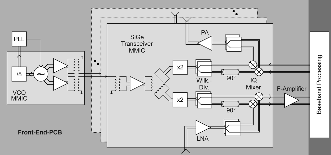
This work focuses on the monolithic microwave integrated circuits (MMICs) and a first circuit board for system demonstration and proof of concept. A block diagram for the developed platform is given in Fig. 1. The implemented MMICs are highlighted in light gray boxes and consist of a VCO MMIC on the left for reference signal generation and a transceiver MMIC on the right for signal up- and downconversion. The VCO MMIC was designed to be used in a phase-locked loop circuit and generates the local oscillator signal for each of the transceiver MMICs. In the system both MMICs are mounted on a common RF substrate PCB to build a first demonstrator board, which is presented in this work. The baseband processing, which is needed to generate the baseband signals, is done using an FPGA. This ensures maximum flexibility with respect to the modulation schemes. The paper is organized as follows. In Section “Circuit design” the considered system concept and the circuit design for the VCO and the transceiver chip is shown. Section System design shows on-wafer-measurements and first system results and Section Experimental results ends this work with a conclusion.
Block diagram of the proposed SiGe radar chipset and radar system.

Circuit design
LO generation
VCO MMIC
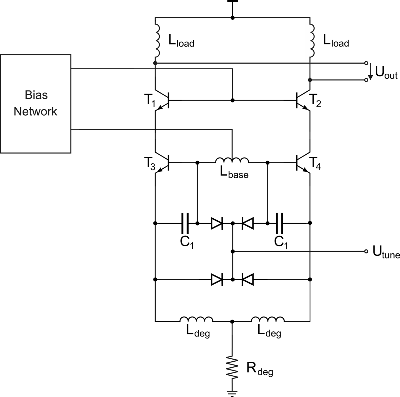
The oscillator architecture was already presented in [Reference Schoepfel, Kueppers, Aufinger and Pohl9] and is based on a differential Colpitts oscillator, as shown in Fig. 2. To simplify the LO distribution toward multiple transceiver MMICs on the circuit board level, the VCO exhibits two single-ended signal outputs which are realized using two differential amplifiers, each followed by a balun load. In addition, a divide-by-8 frequency divider is integrated on the MMIC to allow seamless integration in phase-locked loops using off-the-shelf ICs.
Schematic of the Colpitts oscillator at 38 GHz used in the VCO MMIC.

The measurement results of the VCO presented in [Reference Schoepfel, Kueppers, Aufinger and Pohl9] have suggested that the required tuning range was insufficient for the automotive frequency band from 76 to 81 GHz. For this work the VCO was redesigned by increasing the base inductance L base and the varactor size, resulting in an increase of 8% in center frequency according to simulation.
Frequency doubler and LO distribution
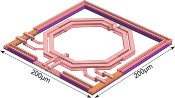
As the active components on the transceiver MMIC have a fully differential architecture, the single-ended LO signal from the VCO is transformed into a differential signal by using the transformer-based balun used in the VCO. In order to drive the mixers on the transceiver with the VCO's LO signal, a frequency doubler and a distribution network is required. To make sure that the VCO delivers sufficient power to saturate the frequency doubler circuits, a preamplifier stage is used. The preamplifier has been implemented as a Common-Base stage using the transformer-based balun on the input of the emitters. This allows direct coupling of the LO signal input into the amplifier while achieving a reasonable wideband input match. The collector load above the Common-Base stage was realized using another transformer shown in Fig. 3. This transformer has two separate windings on the secondary side to distribute the LO signal toward both, the receive and transmit path.
Distributing transformer in the LO distributing network of the transceiver to separate RX and TX.

Using this approach has the advantage of being a fully symmetrical and space-saving distribution network to drive all on-chip components. Other techniques of distributing a differential signal toward separate channels do not offer this symmetry or are much larger in comparison.
The two 100 Ω outputs of this distributing coupler are transformed into a high impedance toward the input of the transformer allowing to increase the overall gain of the input stage and lowering the DC power required to saturate the on-chip components that follow the distribution transformer. Much effort was made on the presented stage to be able to drive as many transceivers as possible from one stabilized VCO. This is very helpful for the use as an LO signal source in a MIMO system. The possible number of channels that can be realized is limited to the available power generated by the VCO. Assuming an ideal 3 dB signal splitter, the generated VCO power can be split four times while still achieving an input power into each transceiver higher than − 10 dBm. Due to the two VCO outputs up to 32 transceivers can theoretically be driven by one VCO MMIC. Taking transmission losses of bond wires and distribution networks into account, the VCO can still feed up to 16 transceiver MMICs.
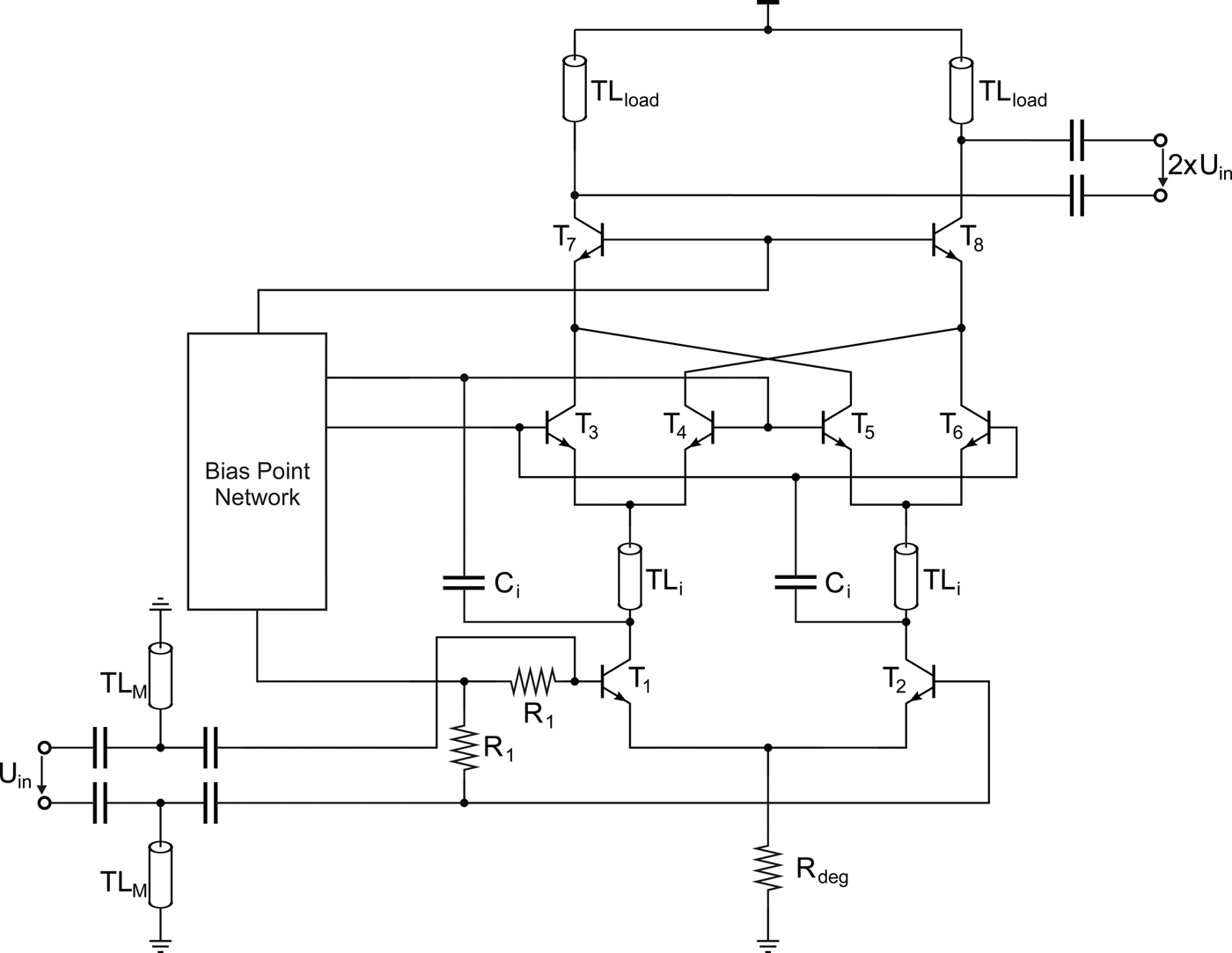
Following the distribution network, the conditioned LO signals each feed a frequency doubler. The frequency doubler is used to cover the automotive band using the 38 GHz-VCO. This architecture is chosen instead of a 76 GHz-VCO to achieve a higher isolation between the VCO and the power amplifier as the frequency doubler acts as an extra isolation stage between the VCO and the PA. Instead of using one common frequency doubler to feed the RX as well as the TX as presented in [Reference Schoepfel, Kueppers, Aufinger and Pohl9], two separate doublers for RX and TX are used. This architecture increases the isolation between the transmitting and receiving channel, while still ensuring a high PA to VCO isolation. The schematic of the used frequency doubler is shown in Fig. 4 and is based on a bootstrapped frequency doubler already presented in [Reference Schoepfel, Kueppers, Aufinger and Pohl9,Reference Kueppers, Aufinger and Pohl10]. Using the bootstrapped doubler, a higher conversion gain can be achieved compared to the standard Gilbert cell doubler. In addition to the information given in [Reference Schoepfel, Kueppers, Aufinger and Pohl9], the doubler was simulated under the aspect of high-order harmonics, as they can potentially cause ghost targets in the radar measurement. Assuming an input frequency into the doubler of 38 GHz, the output signal exhibits a frequency of 76 GHz. Odd harmonics of the input signal do not occur, as the circuits are designed fully differentially. Beside the intended second harmonic, only additional even harmonics can be noticed. But they do not harm the system's performance, as the strongest unwanted harmonic is already attenuated by 30 dB compared to the second harmonic.
Schematic of the frequency doubler at 38 GHz.

The doubler output then feeds the mixer's LO inputs. The mixer's quadrature architecture is achieved, by the use of two separate Gilbert mixer cells. By using two Wilkinson dividers as shown in the block diagram in Fig. 1, both mixer cells can be fed by the LO signal generated by the frequency doubler. A delay line between the LO signal and one Gilbert cell is used to cause a 90° phase shift. By adding aluminum fuses to the delay lines the phase shift can be trimmed after production. This distribution architecture in combination with the VCO MMIC allows driving the mixers with a tunable LO frequency in the automotive band. The presence of higher harmonics can result in an upconverted signal spectrally located at the respective harmonic. To up-convert the IF signal in frequency, a Gilbert cell requires a strong LO signal for driving the switching quad. As the higher order harmonics of the doubler are strongly attenuated and all following circuits are only well matched for the second harmonic, the mixer exhibits a high conversion loss for every other harmonic. Based on simulation, the quadrupled fundamental frequency, which is the first unwanted harmonic, is suppressed by more than 95 dB. Therefore, higher order harmonics caused by the frequency doubler can be neglected in performance considerations.
Transmitter
In Fig. 1 the architecture of the TX path is shown. It contains the quadrature mixer to up-convert the digitally created baseband signals into the automotive band. Following the mixer stage a power amplifier is utilized for a higher maximum output power level of the demonstrator.
Transmit mixer
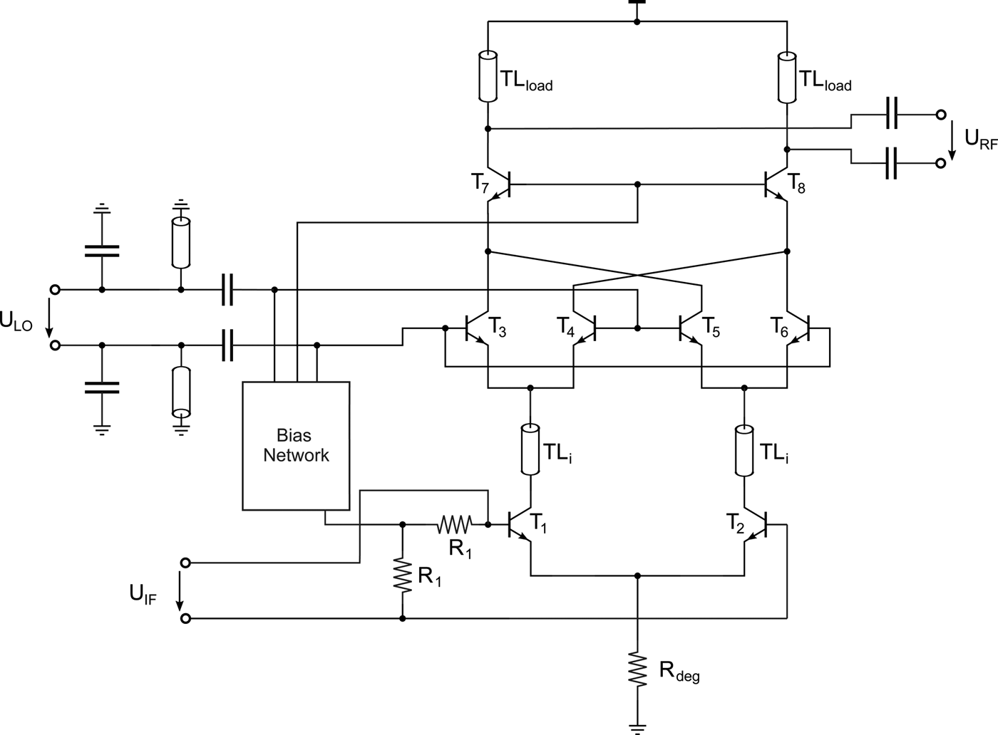
The schematic of the transmit mixer is shown in Fig. 5. A standard Gilbert cell forms the circuit's mixing core. Additionally, a Common-Base circuit is placed above the switching quad of the Gilbert cell to buffer the mixer output for driving a 100 Ω interface toward the power amplifier. The load of the mixer consists of a transmission line to fully utilize the available voltage headroom. The matching of the LO input and the mixer's output is optimized for operation at the LO frequency. The mixer's IF input is realized as DC-coupled while all other ports are AC-coupled. Two of these Gilbert circuits have been used and are driven by the I and Q LO signals to create a quadrature architecture, which enables dual sideband modulation. Before final power amplification, the I and Q signals are combined using Wilkinson Combiners.
Schematic of the transmit mixer at 76 GHz. It consists of a standard Gilbert cell with a stacked Common-Base stage to be able to drive a 100 Ω interface.

Power amplifier
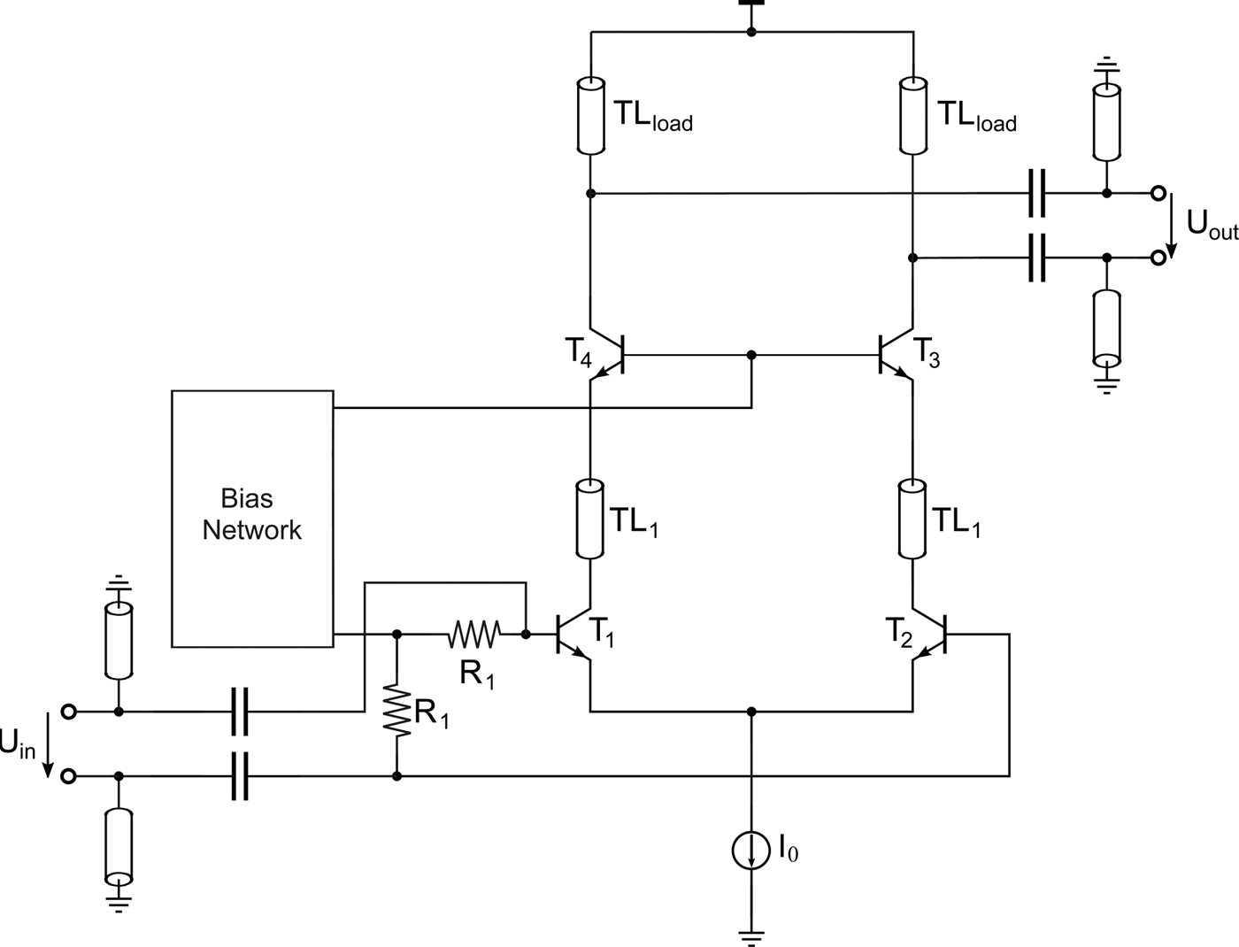
The schematic of the power amplifier is given in Fig. 6. It forms the output stage of the integrated circuit. The main challenge in the design process is the power amplifier's linearity. Considering an OFDM signal as an example of a baseband signal, a high peak-to-average power ratio (PAPR) of the transmitted signal is required. Therefore, the amplifier needs a high linearity performance to prevent the generation of intermodulation products. In order to achieve these requirements, a differential cascode amplifier was chosen. The matching networks for this amplifier are optimized around the 76 GHz carrier frequency. For output matching the capacitive influence of the pads and the inductance of the bond wire have been taken into account achieving a good matching to microstrip transmission lines on the PCB level. As with the upconversion mixer, transmission lines have been used at the collectors to maximize the available voltage headroom. Integrated inductances as those used on the VCO are not used on the transceiver, because at the doubled LO frequency the length of corresponding transmission lines is less critical for a compact design.
Schematic of the power amplifier at 76 GHz. Instead of using a resistor as a current source as presented in [Reference Schoepfel, Kueppers, Aufinger and Pohl9], a current mirror is used to ensure truly differential operation. The core current I 0 in this realization is 56 mA

In addition to this widely-used cascode configuration, the transmission line pair TL 1 is used. To boost the amplifier's gain, TL 1 is placed between the Common-Emitter stage and the Common-Base stage. The additional degeneration presented in [Reference Schoepfel, Kueppers, Aufinger and Pohl9] was not implemented on this MMIC, because it only has a minor impact on the amplifier's performance. Another aspect to achieve high linearity is the reduction of the base contact resistance of the transistors for maximum breakdown voltage of the transistors T 3 and T 4 in Fig. 6. This can be achieved by using multiple transistors in parallel, thus providing the maximum number of base-fingers [Reference Welp, Noujeim and Pohl11].
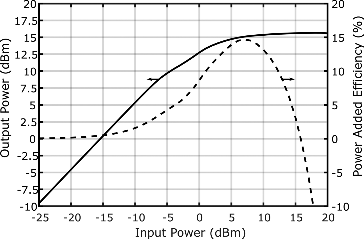
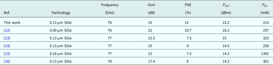
To further improve the performance of the power amplifier, the resistance, used as the current source in [Reference Schoepfel, Kueppers, Aufinger and Pohl9] has been replaced by a current mirror to ensure a more constant core current for truly differential operation. The performance parameters simulated for the PA are presented in Fig. 7. The amplifier saturates at an output referred compression point of 15.2 dBm while offering a linear power gain of 15 dB at a maximum power-added efficiency (PAE) of 15%. In Table 1 these simulations are compared to previous publications on power amplifiers around 76 GHz. In terms of saturated output power the proposed power amplifier is state of the art. Additionally, the presented circuit offers the lowest power dissipation, resulting in the highest PAE.
Simulated compression and power-added efficiency of the proposed power amplifier.

Comparison of the power amplifier to the state of the art. The presented work offers lowest power gain compared to the state of the art, but achieves highest PAE

In the context of a high PAPR, resulting from OFDM modulations, an even higher PAE for lower input power levels is preferable. This could be achieved by using a Doherty-type amplifier stage for example. However, for a first proof of concept demonstrator, the presented PA concept was sufficient.
Receiver
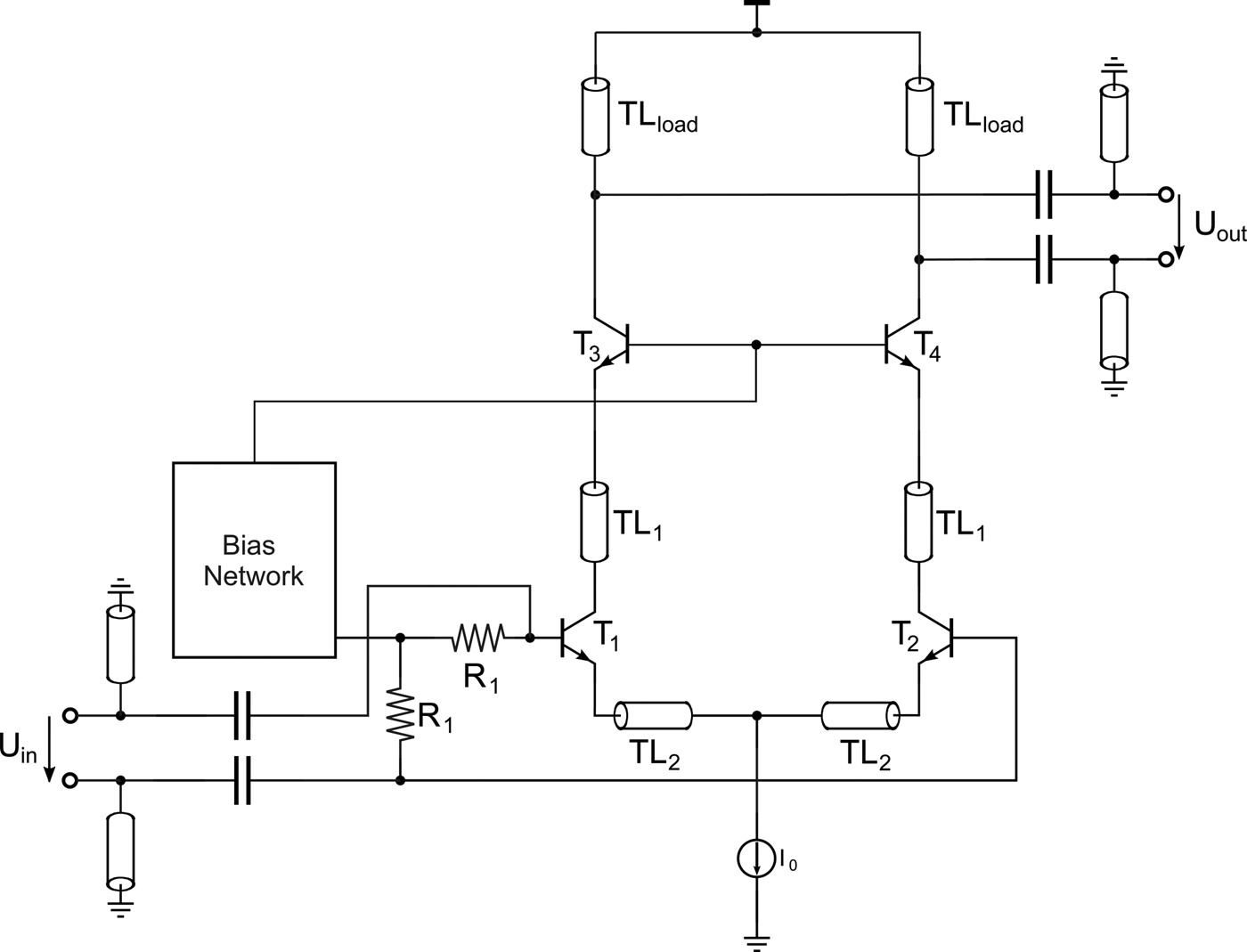
As shown in the block diagram in Fig. 1 the receiver consists of a downconverting mixer in a quadrature configuration and a low noise amplifier (LNA) to improve the noise performance of the receiver chain. The LNA circuit is shown in Fig. 8 and consists of a differential cascode amplifier.
Schematic of the low noise amplifier. The core current I 0 provided by a current mirror-based current source is 15.2 mA.

The transmission lines TL 2 are used as an inductive emitter degeneration to improve the amplifier's linearity. Additionally, the transmission lines TL 1 between the emitter and base stage are used to improve interstage matching resulting in a higher gain. In simulation, the LNA exhibits a noise figure of 5.8 dB while offering a gain of 9.5 dB. Comparing these simulations to literature [Reference Reuter and Yin17], it can be seen that the LNA's performance is state of the art. As already discussed for the TX path, pad capacitance and bond wire inductance have been considered for matching the RX input. The amplifier circuit draws 18 mA from a 3.3 V supply voltage. To split the amplified receive signal for the quadrature mixer cells, the lumped element Wilkinson divider from the LO distribution network has been reused.
Receive mixer
Figure 1 shows the architecture of the quadrature mixer. It consists of two Gilbert mixer cells that are driven by the distributed LO signal exhibiting a phase shift of 90°. The Gilbert cell used for the receiver differs from the one used in the transmit path. In contrast to the Gilbert cell used in the transmit path, a resistive load is used due to the low output frequency. A capacitance in parallel adds a lowpass characteristic to this load to suppress the image frequencies generated by the receive mixer.
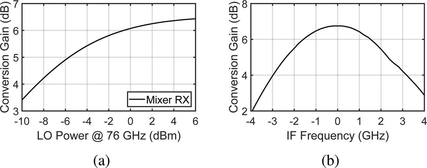
The cascode buffer that is used in the transmit mixer is not suitable for the receiving channel, due to insufficient voltage headroom at the resistive load. Therefore, an emitter follower stage is used to buffer the mixer's output for driving a 100 Ω interface. By using the emitter follower stage as a buffer, a larger voltage headroom is available in the core path. This was used to implement the core current source via a current mirror for better differential performance. According to simulations the whole mixer circuit offers a conversion gain of 7 dB with a noise figure of 11 dB while drawing 15 mA from 3.3 V supply voltage. Compared to current literature the presented mixer offers a lower conversion gain. However, in terms of the noise figure the proposed circuit is state of the art [Reference Reynolds and Powell18,Reference Demirel, Severino, Ameziane, Taris, Bégueret, Kerhervé, Mariano, Pache and Belot19]. In Fig. 9 the simulated conversion gain is shown for varying LO signal power. The simulation shows a LO power of 3 dBm as being sufficient to achieve maximum conversion gain. Also, Fig. 9 shows simulation results on the frequency dependence of the conversion gain. Defining the mixer's bandwidth as the frequency range, where the conversion gain differs by 3 dB, the circuit can be used from 73 to 80 GHz. Thus, the usable frequency range is not limited by the MMIC but rather by the signal processing unit. By integrating the presented circuits into a single MMIC a complete receive and transmit chain has been realized.
Simulated conversion gain in dependence of the LO power (a) and in dependence of the IF frequency assuming a LO frequency of 76 GHz (b).

System design
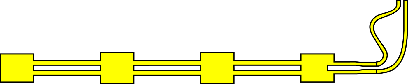
The demonstrator boards for the presented chipset consist of two different PCBs. On the one hand a backend board, that among others holds a commercially available PLL chip to stabilize the VCO-MMIC. This board consists of four copper layers on an FR4 substrate. On the other hand an RF frontend was fabricated as a two-layer board using the Rogers 5880 substrate with an ε r of 2.2. To have sufficient thermal connection for the MMICs, the bottom layer is a 1 mm thick ground layer. One VCO MMIC and two transceiver MMICs have been placed on the top layer, as can be seen in Fig. 12. The receiver output is directly fed into a commercially available differential IF-amplifier to further condition the signal for analog to digital conversion. To radiate the differential transmit signal from the on-chip power amplifier, a differential series fed patch antenna was used [Reference Li, Shao, Cheng and Wang20], [Reference Tong, Wagner, Feger, Stelzer and Kolmhofer21] as shown in Fig. 10.
Geometry of the differential patch antenna.

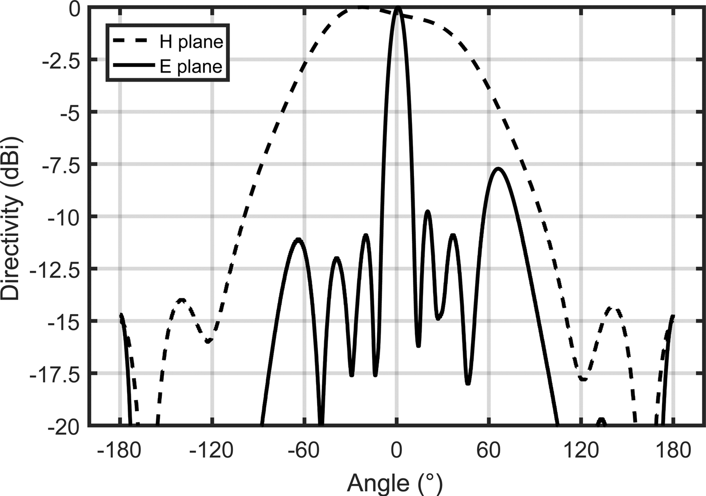
The first of the four series fed patches has a more pronounced slot to match the antenna to the 100 Ω output of the power amplifier. To improve the layout, the antenna was placed at a 90° angle to the MMIC's output on the PCB as shown in Fig. 12. To minimize losses at the transition from the MMIC toward the antenna feed, a transmission line has been added at the feed to the antenna to realize the 90° angle, as can be seen in Fig. 10. A simple differential transmission line is not suitable, due to the difference in line length resulting in a significant phase shift across the two conductors. This phase shift can result in the generation of unwanted polarizations at the antenna elements. To prevent the antenna from radiating in unwanted polarizations, the feeding line exhibits a compensation to lengthen the inner line. The simulated pattern of the proposed antenna architecture in both planes is shown in Fig. 11.
Pattern of the proposed differential patch antenna including the length compensated feeding structure.

Frontend board with two transceiver MMICs and one VCO MMIC.

Experimental results
On-wafer measurement
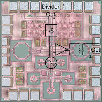
For verification and characterization on-wafer measurements of the circuits presented in Section (Circuit design) have been performed. The die area of the VCO-MMIC is 930 × 930 μm2 and the area of the transceiver MMIC amounts to 1964 × 1448 μm2. In Figs 13 and 14 photographs of the chips are shown with the main components being highlighted.
Chip photograph of the VCO MMIC with overlayed schematic.

Chip photograph of the transceiver with overlayed schematic.

In Fig. 13 the layout of the VCO is shown. In the lower middle of the photograph, the VCO core containing the integrated inductors can be seen. The VCO's single-ended outputs are placed at the right and left edge of the MMIC. At the top edge, the output of the divide-by-8 stage and supply pads are located.
In the upper half of Fig. 14, the LO feeding network of the transceiver-MMIC can be seen. It is designed fully symmetrically to ensure a phase-stable LO distribution into the RX and TX path.
In the lower half of Fig. 14 the left side of the chip contains the RX and the right side contains the TX chain. In the center of the chip another fusable row of contacting pads was provided to allow measurement of on-chip signals feeding the mixer.
VCO MMIC
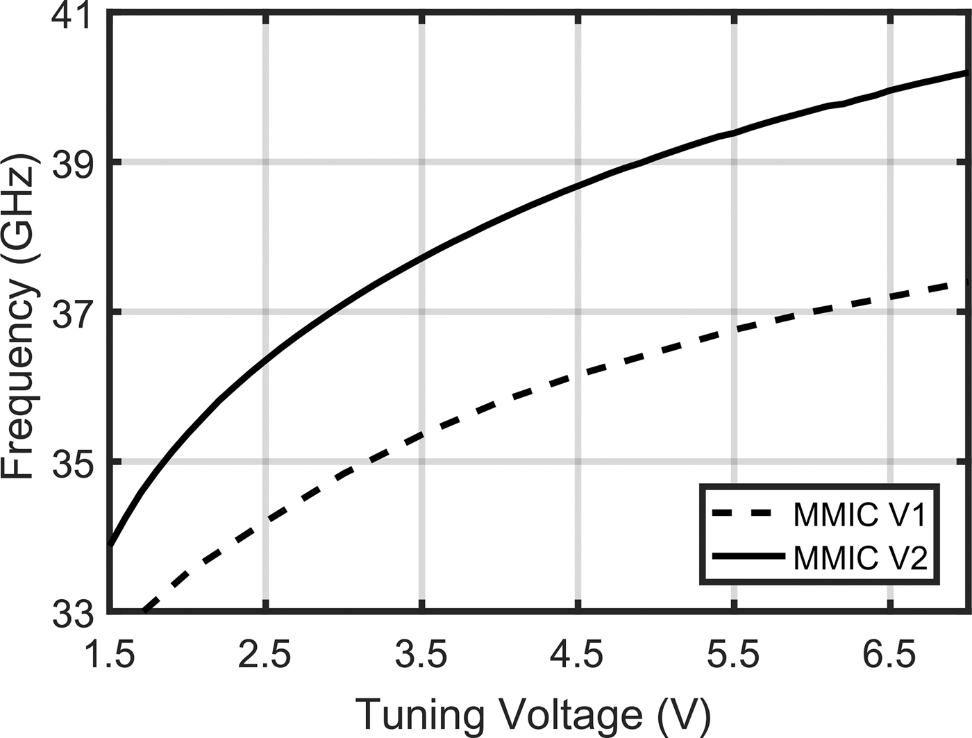
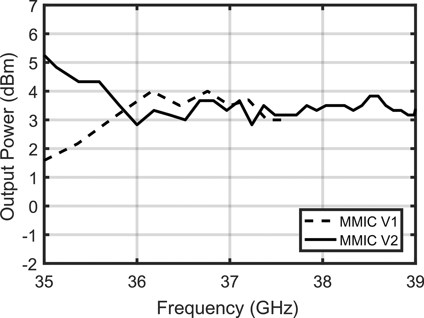
For on-wafer characterization of the VCO-MMIC, RF-probes in GSG configuration have been used to contact the VCO's outputs. The chosen setup enables the measurement of output power and frequency simultaneously. The DC supply, the tuning port, and the enabling IOs were contacted with a multicontact probe. In this configuration tuning characteristics of the VCO were measured at a room temperature of 25°C. During operation the MMIC consumes 45 mA from a 3.3 V voltage source. Figure 15 shows a frequency tuning range of 6 GHz around a center frequency of 38 GHz. This shows that the adjusted base inductance and the increased varactor size result in the desired change in frequency range while the oscillator's output power remains unchanged at a minimum of 3 dBm as shown in Fig. 16.
Measured frequency versus tuning voltage for the VCO chip generations. The insufficient frequency of the first MMIC generation is successfully adapted in the second generation.

Measured output power versus frequency for the VCO chip generations. It shows a variation of the output over the frequency by less than 1 dB inside the desired band.

Transceiver MMIC
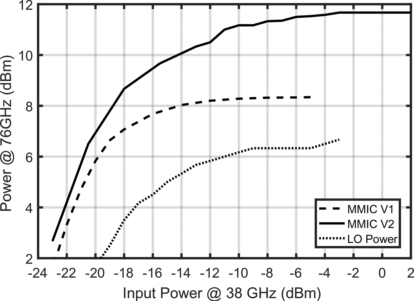
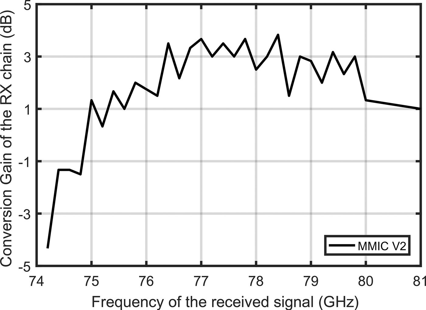
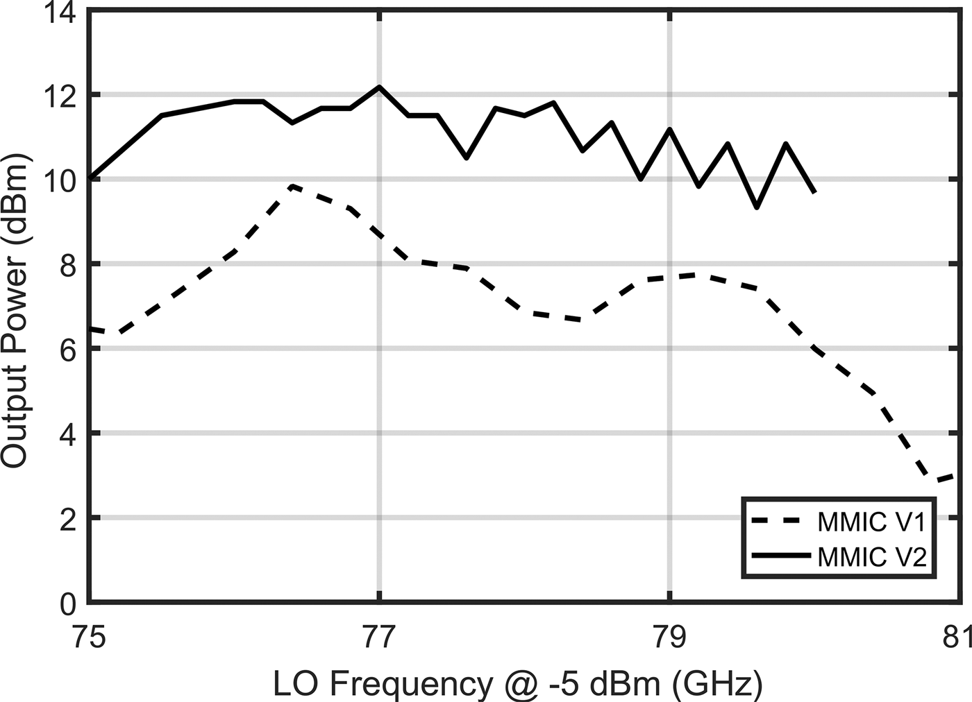
In addition to the VCO-MMIC, the transmit-chain of the transceiver MMIC was characterized with on-wafer measurements. The probe setup consisted of an RF-probe for the differential output of the power amplifier in a GSGSG-configuration. Another RF-probe in GSG-configuration was used at the LO-input to deliver a 38 GHz LO signal. In contrast to the transceiver presented in [Reference Schoepfel, Kueppers, Aufinger and Pohl9], the padframe is fully symmetrical. Because of this, only one DC-probe is required to supply the MMIC and to configure the enable signals. A fourth probe in GSG configuration is placed on the mixer's input pads. In this configuration the minimum VCO power that is needed to saturate the frequency doubler in the LO generation chain was examined by varying the input power applied to the LO input of the chip. Figure 17 shows the results of this measurement. The solid curve shows a saturated output power of 11.5 dBm at the doubled frequency. Furthermore, it was verified that a LO power of − 12 dBm is sufficient to saturate the doubler achieving the maximum LO power to drive the mixers. The dashed curve describes the output power that was measured at the first MMIC presented in [Reference Schoepfel, Kueppers, Aufinger and Pohl9]. Comparing both MMIC versions, a 3 dB higher output power can be achieved with the second version, while still being very sensitive at the LO input. With the VCO delivering 3.5 dBm of output power, up to 16 transceivers can be fed from one stabilized VCO. Comparing the achieved output power of the second transceiver version with the PA's simulated maximum output power of 15 dBm, a deficit of 3 dB in output power is noticeable. This can be justified by the mixer's compression point, because only − 3 dBm of output power can be achieved with the upconverting mixer. Therefore, the PA needs to be able to operate with only − 3 dBm of input power, resulting in a maximum output power of 12 dBm. Figure 19 shows the saturated output power over the LO frequency for both MMIC versions. It can be seen that the output power is increased from the previous version and that the amplitude variation over frequency is decreased in the second MMIC generation. Finally, a measurement verifying the LO power, which supplies the quadrature mixer, was carried out. A probe in GSGSG configuration was placed on the fusable pads, while externally feeding the LO signal with a signal generator. The measured result is shown as the dotted line in Fig. 17. From this diagram it can be seen that an LO power of 6 dBm can be achieved feeding the LO input of the transmit mixer. As the LO distribution is fully symmetrical, the same power can be expected at the LO input of the receive mixer. According to simulation an LO power of 6 dBm is sufficient to ensure that the mixer's switching quads work properly as was already shown in Fig. 9. To complete the transceiver characterization, another measurement for the RX path was carried out. For this measurement an RF probe in GSGSG configuration was placed at the receiver's input while still feeding the LO input of the transceiver chip externally. By feeding the receiver with a continuous wave signal with a frequency slightly offset from the LO signal, an IF signal is generated that can be measured at the mixer's output pads via a probe in GSG configuration. The remaining signal pad of the receiver input was externally terminated with a 50 Ω load. With this setup the performance of the receiver chain is characterized. In Fig. 18 the conversion gain of the chain is shown over frequency of the received signal. It can be seen that the chain is well matched in frequency as it offers maximum performance around the desired frequency of 76 GHz. In summary the presented chipset is sufficient for a first demonstrator to prove the basic concept.
Measured output power versus the input power fed into the LO generation stage of the transceiver chip.

Measured conversion gain over the frequency of the RF signal at the mixer's input.

Measured output power of the transmitter path for varying LO frequency.

System results
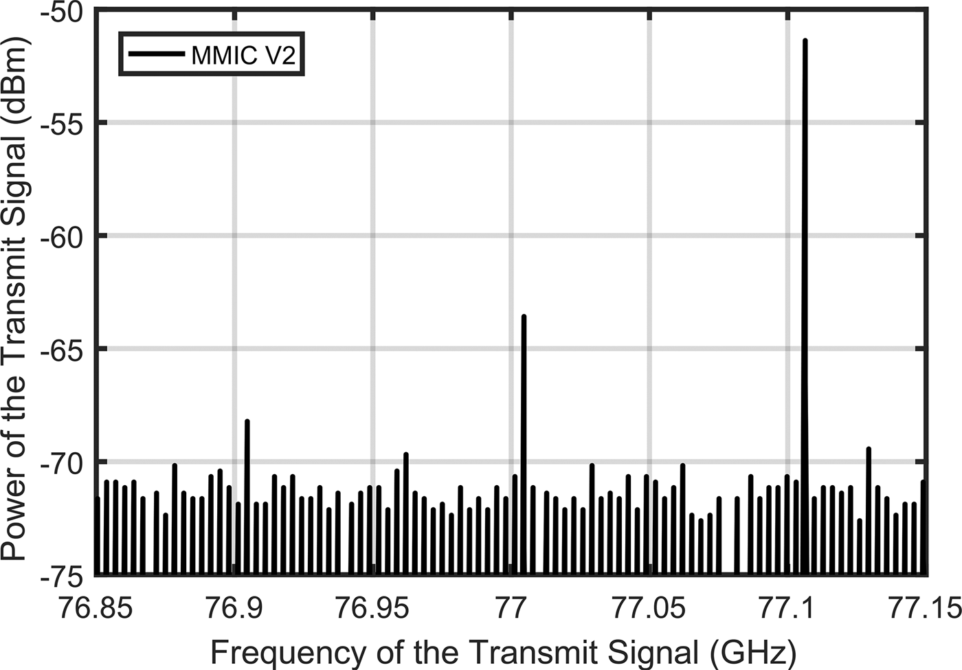
After proving functionality of the chipset with on-wafer measurements, the whole system has been tested. To verify the transmitter chain, a two-port signal generator was used to feed the TX mixer with two sine signals with a frequency of 100 MHz and a 90° phase shift. By using a horn antenna the transmitted signal has been fed into a spectrum analyzer. The resulting measurement is shown in Fig. 20. It can be seen that a sideband suppression of 17 dB was achieved. Furthermore, an LO suppression of more than 10 dB can be noticed.
Measured spectrum of the transmitted signal. A sine of 100 MHz in 0 –90° phase is modulated on the LO at 77 GHz.

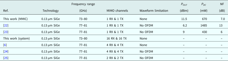
By varying the phase difference of the generated sinus signals, a change in sideband suppression was observed. Additionally, alternating the sign of the phase difference resulted in suppression of the corresponding sideband. These results show that the basic quadrature architecture of the mixer is fully functional and working as designed. Further investigations on the sideband suppression have to be carried out as the phase difference of the I and Q LO signal can be adjusted by trimming the designated fuses in the delay lines. Thus, the LO suppression can potentially be increased. Considering the presented system compared to other work on this field, a distinction must be made between the system level and the chip level. A comparison is shown in Table 2. On chip level the presented transceiver is state of the art. In terms of output power and noise figure, the transceiver reaches the performance of MMICs presented in current literature. Comparing the maximum output power, the presented MMIC exceeds the state of the art. On system level, this chipset offers a benefit compared to other systems, as the presented LO distribution network enables a higher number of MIMO channels.
State of the art comparison. Rows 1–3 contain a comparison on the chip level, while the remaining rows include a system-level comparison

Conclusion
This paper presents two SiGe MMICs, implemented in the same technology that work at 3.3 V. The realized VCO-MMIC has a frequency tuning range of 6 GHz and can be used as a signal source for the radar system. The second MMIC contains a complete transmit and receive chain at 76 GHz. During on-wafer measurements the functionality of the whole set of MMICs has been verified. A fully functional system has been build by integrating the MMICs onto an RF PCB. A comparison to other work on this field is shown in Table 2. The comparison is divided into two parts. At first only one channel transceiver MMICs are compared. In addition, the presented system is compared to other publications. It can be seen that this work is state of the art in terms of the MMICs with main advantages of not having any limitation toward the waveform of the signal and a higher output power. When comparing the work on system level, the presented LO distribution network enables a higher number of possible MIMO channels compared to the state of the art. Furthermore, the comparison illustrates the flexibility for handling any kind of modulation scheme, where most of the compared work is limited. In the future work further investigation on the performance of the MMICs and the demonstrator PCBs is planned. In addition, new demonstrator PCBs with substantially more MIMO radar channels are the goal of further work.
Author ORCIDs
Jan Schoepfel, 0000-0002-4009-4924
Acknowledgments
The authors gratefully acknowledge the German Federal Ministry of Education and Research for partially funding this research in the project radar4FAD. Additionally we want to thank Infineon Technologies AG and its staff members for fabricating the chips.
 Jan Schoepfel received the B.Sc. and M.Sc. degrees in electrical engineering and information technology from Ruhr University Bochum, Bochum, Germany, in 2014 and 2016, respectively. Since 2017, he has been with the Institute for Integrated Systems, Ruhr University Bochum, Bochum, Germany. His current research interests include the concepts and integrated circuits for radar sensors for fully autonomous driving.
 Simon Kueppers was born in Oberhausen, Germany in 1988. He studied electrical engineering and received the Bachelor of Engineering degree in 2008 and the Master of Science degree from Ruhr University Bochum, Germany in 2014. In 2015, he became a Researcher at the Fraunhofer Institute for High-Frequency Physics and Radar Techniques FHR in Wachtberg, Germany focusing on millimeter-wave MIMO radar systems. From 2018 on, he is continuing his work in the same field toward his Ph.D. and is currently employed at 2pi-Labs GmbH, Bochum, Germany.
 Klaus Aufinger was born in Kirchbichl, Austria, in 1966. He received the Diploma and the Ph.D. degrees in physics from the University of Innsbruck, Innsbruck, Austria, in 1990 and 2001, respectively. In 1991, he joined the Corporate Research and Development of Siemens AG, Munich, Germany, where he investigated noise in submicrometer bipolar transistors. He is currently with Infineon Technologies, the former semiconductor group of Siemens, Munich, working in the field of device physics, technology development, and modeling of advanced SiGe technologies for high-speed digital and analog circuits.
 Nils Pohl received the Dipl.-Ing. and Dr. Ing. degrees in electrical engineering from Ruhr University Bochum, Bochum, Germany, in 2005 and 2010, respectively. From 2006 to 2011, he was a Research Assistant with Ruhr University Bochum, where he was involved in integrated circuits for millimeter-wave(mm-wave) radar applications. In 2011, he became an Assistant Professor with Ruhr University Bochum. In 2013, he became the Head of the Department of mm-wave Radar and High Frequency Sensors with the Fraunhofer Institute for High Frequency Physics and RadarTechniques, Wachtberg, Germany. In 2016, he became a Full Professor for Integrated Systems with Ruhr University Bochum. He has authored or co-authored more than 100 scientific papers and has issued several patents. His current research interests include ultra-wideband mm-wave radar, design, and optimization of mm-wave integrated SiGe circuits and system concepts with frequencies up to 240 GHz and above, as well as frequency synthesis and antennas. Dr. Pohl is a member of VDE, ITG, EUMA, and URSI. He was a corecipient of the 2009 EEEfCom Innovation Award, the 2012 EuMIC Prize, and the 2015 Best Demo Award of the IEEE Radio Wireless Week, and a recipient of the Karl-Arnold Award of the North Rhine-Westphalian Academy of Sciences, Humanities and the Arts in 2013 and the IEEE MTT Outstanding Young Engineer Award in 2018.