Introduction
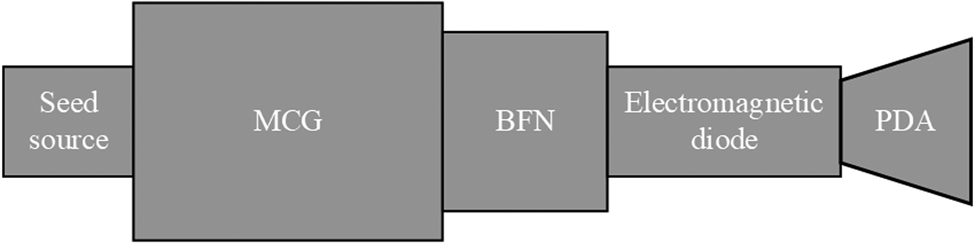
Electromagnetic diodes need a directive radiation pattern to affect a specific target point effectively [Reference Hosseini, Sadeghzadeh and Aliakbarian1]. Electromagnetic sources usually use a single shot. The single-shot, high-energy, and high-voltage pulsed source has to apply high amounts of delivered energy to electromagnetic sources. The best solution to this requirement is a magneto-cumulative generator (MCG). A block diagram of an high power microwave (HPM) generator is shown in Fig. 1.
Block diagram of an HPM generator.

In the block diagram, the seed source feeds the stator coil of an MCG, which creates a powerful magnetic field. The MCG output is connected to a pulse forming network that provides transformation of heavy current to a high impulse voltage, which feeds a high-power electromagnetic diode. The generated microwave is emitted through PDA into space. A coaxial-vircator (coaxial virtual cathode oscillator) is an electromagnetic diode capable of converting a narrow pulse to a narrow-band microwave signal at high power levels. They have many military and civilian applications. The coaxial-vircator and PDA are subsystems of the HPM generator [Reference Biswas2–Reference Shao, Liu, Yang, Chen, Song and Huang4]. Note that some electromagnetic diodes have Transverse electromagnetic (TEM) or TM01 mode outputs [Reference Tribak, Zbitou, Mediavilla Sanchez and Amar Touhami5,Reference Jiang, He, Zhang, Li and Ling6]. For example, the magnetically insulated line oscillator (MILO) and coaxial-vircator generate fields in TEM and TM01 modes [Reference Hosseini and Oraizi7,Reference Lee, Lee, Yoon and So8], respectively, which is not suitable. A horn antenna or an open-ended waveguide radiating these modes to generate donut-shaped patterns cannot affect a target point effectively. However, many mode converters have been designed and manufactured.
The oldest and most important is the Vlasov antenna. A diagonal cut at the end of the open aperture waveguide creates a Vlasov antenna. The main beam of the antenna has an angle of about 30° to the boresight. So, it is not usable in some applications. Besides, the shape of the output pattern is strongly dependent on the cutting angle of the waveguide. But it focuses the maximum power in the center of the diagonal section aperture in a too narrow band [Reference Misilmani, Al-Husseini, Kabalan and El-Hajj9–Reference shen Ling and Yuan12]. This problem is more noticeable in the coaxial-vircator because its frequency is a function of the applied voltage [Reference Vladimir, Tamara, Alexey, Vera and Gennady13, Reference Betzios and Uzunoglu14]. Another method to realize a linear mode converter is to insert metal plates inside a coaxial waveguide. The metal plates divide the coaxial waveguide into sectorial waveguides with different phase velocities. It can transfer the maximum waveguide power to the waveguide center in a small bandwidth (less than 500 MHz) and then transmit it into space using a horn antenna or an open-ended waveguide. The major problem is that if it is designed at high frequencies, it will cause a significant increase in length [Reference Hosseini, Sadeghzadeh and Aliakbarian1] and [Reference Hosseini, Dahmardeh and Yousefian15–Reference Yuan, Liu, Zhong, Qian and Li23]. The coaxial beam-rotating antenna (COBRA), which uses a dielectric to change the input mode, is the other mode converter. The main problems are unusable in HPM and large SLLs [Reference Lee, Ahn, Yoon and Lee24–Reference Li, Deng, Guo, Huang and Shao31].
In the electromagnetic diodes, conversion of a donut-shaped pattern into a directive pattern by mode converters dramatically increases the total losses, weight, size, and cost [Reference Hosseini, Sadeghzadeh and Aliakbarian1]. Besides, the very low bandwidth of mode converters prevents them from being used in broadband systems. When testing an electromagnetic diode, the frequency may change dramatically. This change is much more noticeable in the electromagnetic diodes wherein the frequency is a function of the voltage applied. We propose a novel antenna we call the pattern director antenna (PDA) to solve most of the problems associated with the azimuthally symmetric output modes of high-power microwave sources. The PDA accepts directly (without the need for mode conversion) a generated azimuthally symmetric mode of an electromagnetic source and radiates a directive pattern. PDAs may not be compared with mode converters, wherein the goal is to convert the modes with zero field intensity in the center to modes with maximum field intensity. It is usually not possible at wide frequency bandwidth. But in PDA, the goal is to convert the donut-shaped pattern into a directive pattern. Hence, the bandwidth increases significantly. In the measurement of electromagnetic diodes, since the frequency is a function of the applied voltage, the frequency may severely change with each shot. The generated wave should not be filtered by the antenna. The PDAs can also be used as a broadband antenna in the final design of HPM generator.
Most ultra-wideband (UWB) antennas, such as the Vivaldi [Reference Arezoomand, Sadeghzadeh and Naser-Moghadasi32, Reference Arezoomand, Naser-Moghadasi, Arghand, Jahangiri and Zarrabi33] and ridge horn [Reference Isenlik, Basaran and Turetken34], are designed and fabricated for low power applications, so they are not suitable for use in the output of HPM sources. In addition, the inlet structure of these antennas is not befitted for use as a radiation subsystem in the HPM generators.
This paper presents a novel antenna (we call PDA) that solves the radiation problems of HPM generators. The square-shaped pattern director antenna (SPDA) does not have the previous mode converter problems and has a wide bandwidth.
Section “SPDA structure” presents the theory. In section “Design of SPDA,” the SPDA is designed in detail. In section “SPDA simulation,” the simulation of the SPDA is presented. The results of the simulations are also fully explained. Section “Implementation of SPDA” focuses on the fabrication of the SPDA. In this section, its fabrication by 3D printing technology is described. Section “SPDA measurement” presents the measured results. All measurement data are compared with the simulation results with good agreement. Finally, the conclusions are presented in section “Conclusion.”
SPDA structure
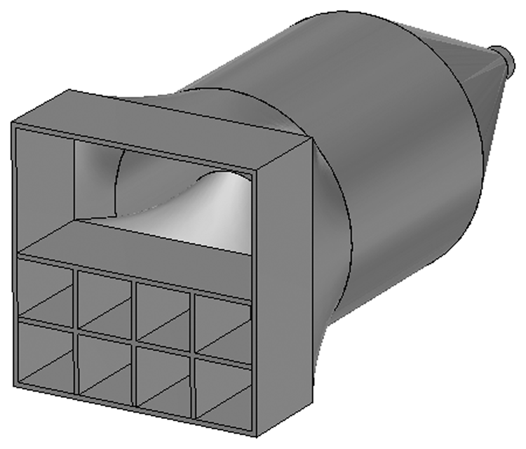
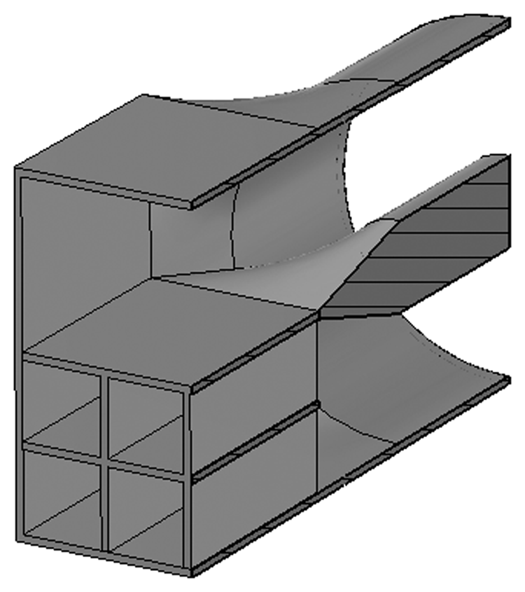
Figure 2 shows the simulated SPDA.
SPDA structure.

As shown in Fig. 2, the SPDA consists of a circular waveguide connected to a square waveguide with a window aperture. The circular waveguide is a replacement for the electromagnetic diode that produces TEM mode. The circular waveguide is converted to the square waveguide by the conversion section, which is due to the proper placement of square waveguides in the lower part of the SPDA aperture. The central core is also converted into a plate by a size conversion section. Finally, two rectangular waveguides are created. The lower rectangular waveguide is divided into eight similar square waveguides.
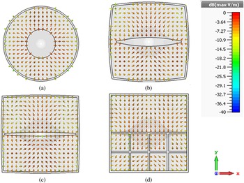
In Fig. 3, step A depicts the electric field pattern at the beginning of the cylindrical waveguide, which acts as a TEM-stimulated electromagnetic diode. From this point on, the body and core of the SPDA move from a circular cross-section to a rectangular. Step B shows the electric field pattern at the desired plate from the conversion section of circular to rectangular waveguides. Note that the electric fields in the upper and lower waveguide sections are 180° out-of-phase.
Electric fields in the SPDA.

When the upper and lower waveguides are in phase, the output pattern becomes directional. It is the operating principle of PDA and will cause the electric field to be in phase in the antenna aperture. Step C shows the input part of the square section. In this section, the fields in the upper and lower waveguides are separated by a conductor blade. Also, they have 180° phase difference. Step D shows the electric fields of the antenna aperture.
Design of SPDA
The inlet test structure is made of a conical frustum. It is to convert the dimensions of a cylindrical waveguide, equivalent to an electromagnetic diode, to a standard N-type connector. The frequency and the impedance determine the frustum length.
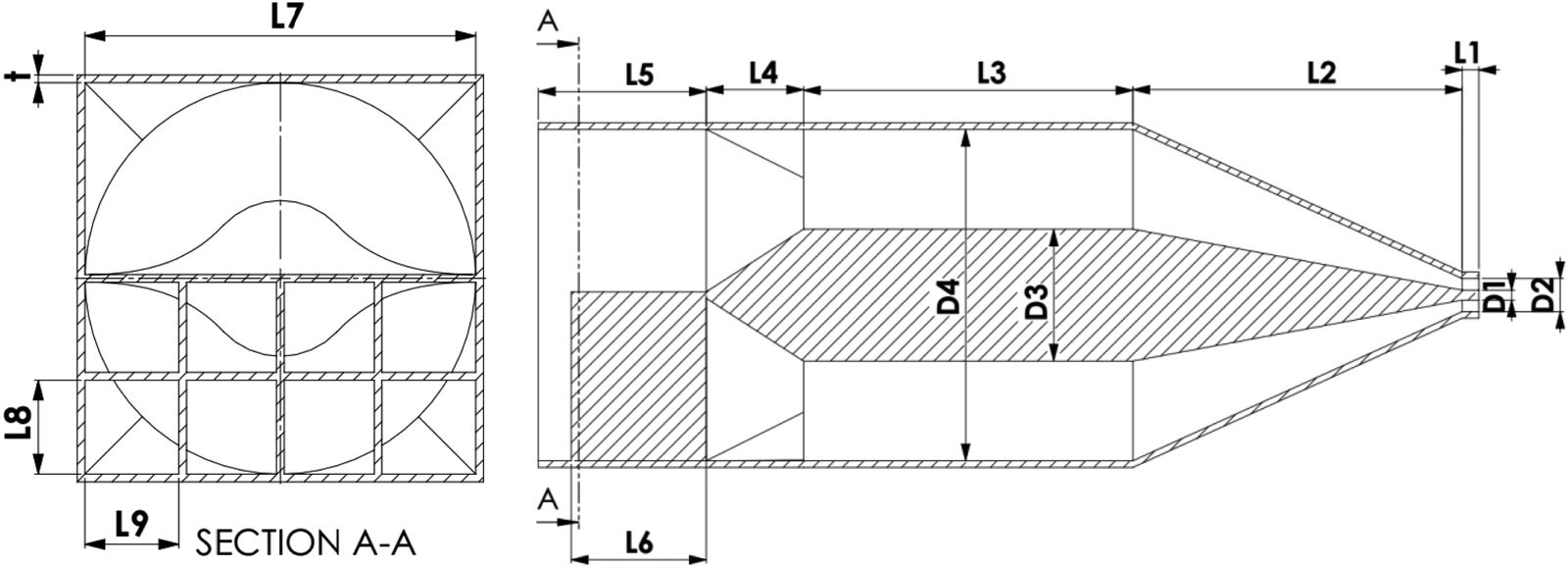
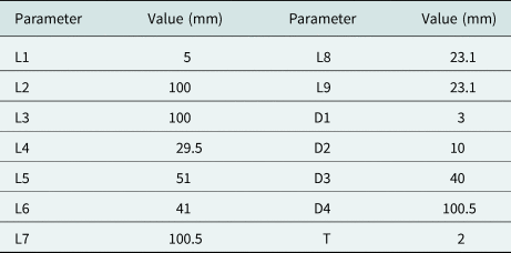
In Fig. 4, the field in TEM mode is injected into the SPDA by the standard N-type connector. Table 1 presents the dimensions of SPDA after optimization.
Dimensions of the SPDA.

Dimensions of the SPDA

Now, we would like to calculate the dimension L6 in Fig. 4. According to the dimensions of the waveguides given in Table 1, L6 can be calculated using the concept of the phase constant and the FEM method. Hence, the phase constant of the square waveguide and the rectangular waveguide is calculated by the FEM method. The obtained values of the phase constant for rectangular and square waveguides are as follows.


Note that these values are calculated at the center frequency (7.5 GHz). According to the values obtained for the phase constant, the length of the mode conversion section (L6) can be calculated as [Reference Hosseini, Sadeghzadeh and Aliakbarian1].

To calculate the minimum length, n = 1. Therefore, by inserting the phase constant values in (1), we have L6 ≈ 41 mm.
SPDA simulation
The SPDA is simulated by CST version 2021 software. In Fig. 5, the cut-off view of SPDA is shown.
Cut-off view of the SPDA.

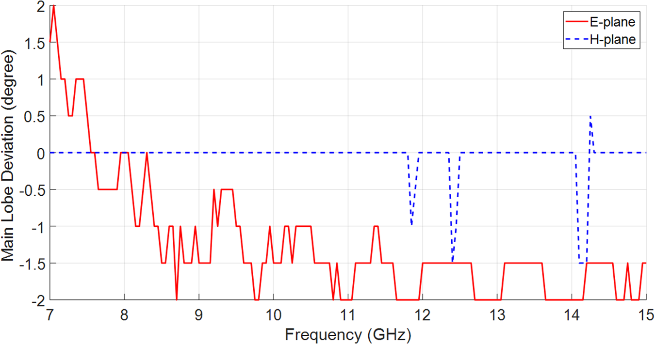
The structure is simulated based on the values optimized for a directive pattern. The significant results of the SPDA contain the return loss, radiation pattern, gain, SLL, and MLD from the antenna boresight. The main beam deviation from the boresight is the most important PDA parameter. Too deviations will cause the antenna to focus on another direction and point.
According to Fig. 6, the deviation of the main lobe from the antenna boresight at the center frequency is about zero degrees.
Simulated results of the MLD from the boresight at the E and H plates.

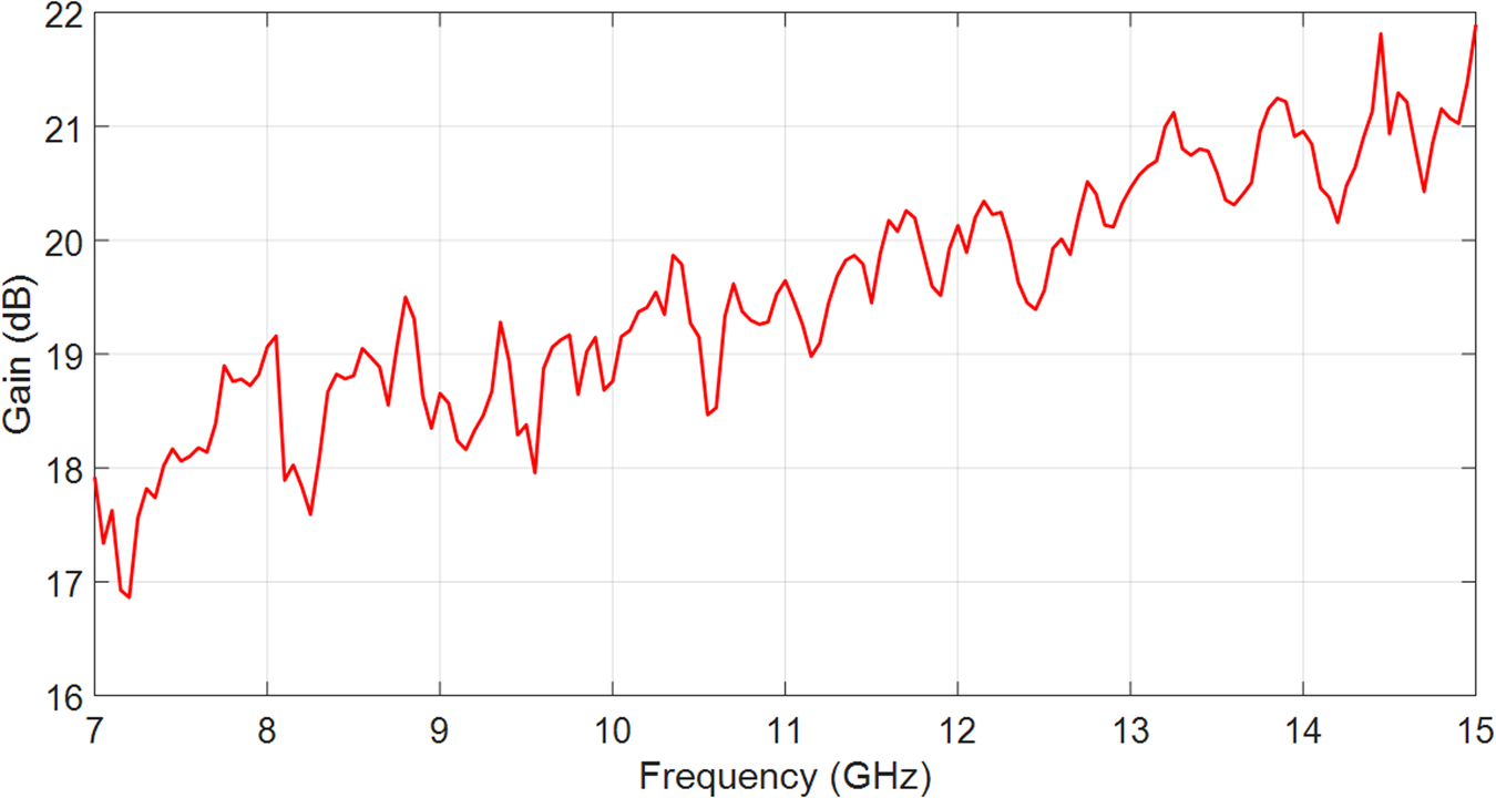
In Fig. 7, the antenna gain is shown in the frequency range. It is more than 20 dB at the center frequency. It also is more than 16.8 dB in the bandwidth. Note that increasing the frequency increases the gain.
Simulated gain result of the SPDA.

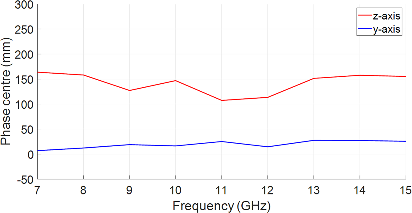
The phase center of UWB antenna affects the performance in the time domain. Usually, the width of transmitted impulse is about several hundreds of nanoseconds, so even fine phase center shift greatly will influence the phase of far-field and lead to the waveform dispersion in the time domain [Reference Arezoomand, Sadeghzadeh and Naser-Moghadasi32, Reference Arezoomand, Naser-Moghadasi, Arghand, Jahangiri and Zarrabi33].
As shown in Fig. 8, the phase center changes between 107.49 and 163.29 mm and 12.28 and 25.6 in the z and y axes, respectively. Due to symmetry, the phase center in the x-axis is always constant and equal to zero. Therefore, it shows a linear phase center with negligible variation in the frequency band of 7–15 GHz. Hence, the SPDA is fit for radar applications, too.
Simulated phase center result of the SPDA.

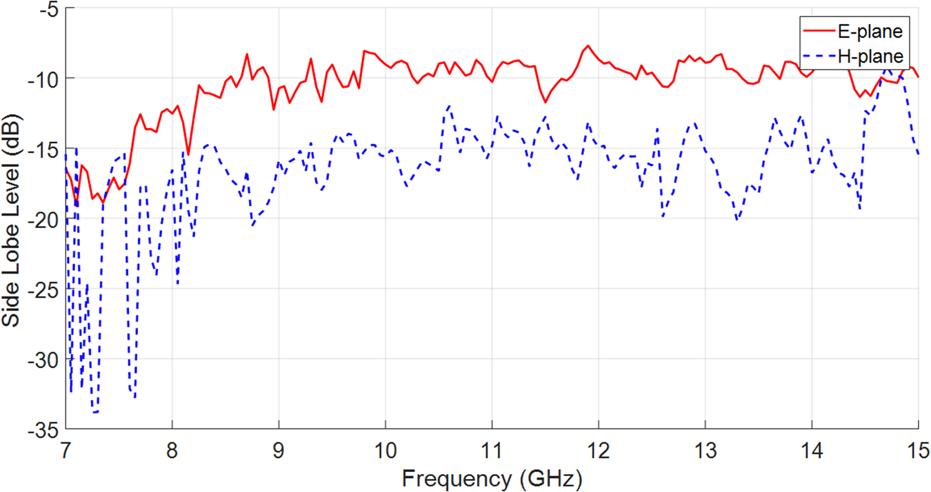
Due to the large aperture size and high frequency, the SLL is a significant characteristic. The SLL is less than −7 dB in the frequency range. Figure 9 shows the SLL of the SPDA.
Simulated results of the SLL at the E and H plates.

Implementation of SPDA
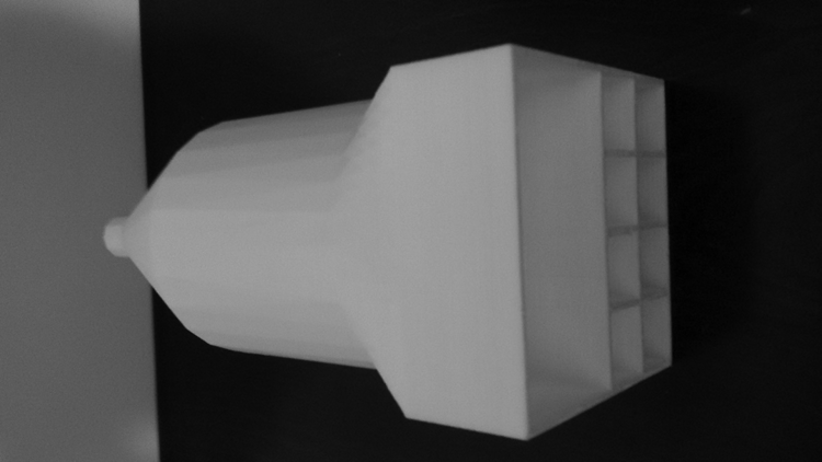
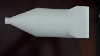
The SPDA is fabricated as designed. 3D printing technology has been used to increase the accuracy and reduce the cost of the fabricated model. A polylactic acid (PLA) is used to fabricate the antenna. PLA does no damage to the natural environment because it comes from renewable sources such as corn flour, sugar cane, cassava root starch, and potato starch [Reference Guo, Shang, Lancaster and Xu35–Reference Helena, Ramos, Varum and Matos42]. Figure 10 depicts the model fabricated by the 3D printer.
SPDA made by the 3-D printer.

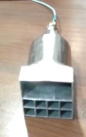
After fabrication, the structure is covered by a thin aluminum layer to convert the antenna surface to a conductor. Figure 11 shows the coated structure.
Antenna coated with aluminum.

Antennas are usually fed by specific feed structures [Reference Yousefian, Hosseini and Dahmardeh43–Reference Hosseini45]. To apply a signal to the SPDA, a simple feed system composed of two conical frusta section is used. This section is employed to match the input impedance to a standard N-type connector. The filled and hollow conical frustum is used as the core and body, respectively. The top base of conical frusta dimensions is equal to the standard N-type connector. This section is depicted in Fig. 12.
Antenna feeding section.

SPDA measurement
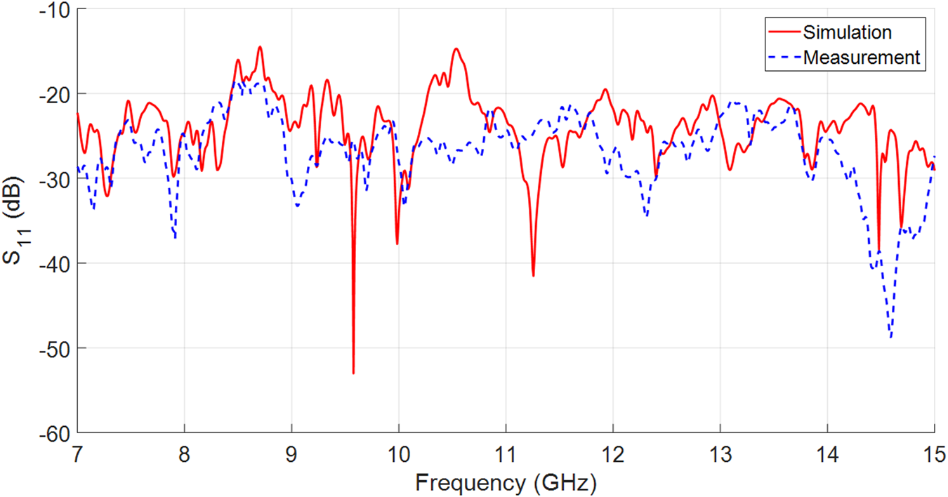
The antenna return loss and radiation pattern are measured in the frequency band. Figure 13 shows the results of the simulation and measurement of the S 11.
Simulated and measured results of the S 11.

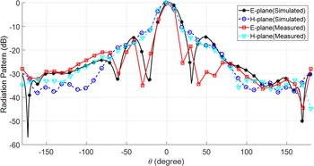
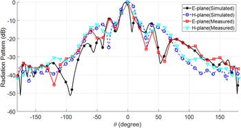
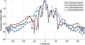
According to Fig. 13, S 11 in the frequency bandwidth falls in the acceptable range, which verifies the proper design of the structure. In Figs 14–16, the antenna patterns are shown in the E- and H-planes at the three frequencies.
Radiation pattern at the 7 GHz frequency.

Radiation pattern at the 11 GHz frequency.

Radiation pattern at the 15 GHz frequency.

Conclusion
In this paper, the antenna is designed, simulated, fabricated, and measured at the frequency 8 GHz (namely 6–9 GHz frequency bandwidth). The antenna converts a donut-shaped radiation pattern of the electromagnetic source to a directive pattern. We call it a SPDA. The simulated and measured results of the SPDA are acceptable. 3D printing technology is used to make it cost-effective. The gain in the SPDA changes from 16.8 to 21.8 dB in the specified frequency band. The antenna can be used for both TEM and TM01 input modes. The antenna is best used for electromagnetic sources, with favorable frequency and size characteristics. Also, the frequency is a function of the voltage applied to the electromagnetic diode. The S 11, MLD, and SLL are less than −15 dB, 2°, and −7 dB, in the frequency range, respectively. As shown in this paper, the simulation results are in good agreement with the measurements.
 Seyed Jalil Hosseini received the MS degree in 2016 in Electrical Engineering from Khajeh Nasir Toosi University of Technology (KNTU), Tehran, Iran. He is currently studying for a Ph.D. with major in communication systems at the Electrical Engineering Department, Iran University of Science and Technology (IUST), Tehran, Iran. His research interests are antenna design, mode converters, beam scanning technology, waveguide design, electromagnetic field measurement instrumentation, and radiation system design.
 Homayoon Oraizi (LSM'14) received the B.E.E. degree from the American University of Beirut, Beirut, Lebanon, in 1967 and the M.Sc. and Ph.D. degrees in electrical engineering from Syracuse University, Syracuse, NY, USA, in 1969 and 1973, respectively, From 1973 to 1974, he was a Teacher with the K. N. Toosi University of Technology, Tehran, Iran. In 1985, he joined the School of Electrical Engineering, Iran University of Science and Technology, Tehran, where he is currently a Full Professor of electrical engineering. In 2003, he spent a two-month term with the University of Tsukuba, Tsukuba, Japan, where he spent a six-month sabbatical leave from 2004 to 2005. He is also an Invited Professor with the Electrical Engineering Group, Academy of Sciences of Iran, Tehran. He has authored or coauthored more than 300 articles in international journals and conferences. His current research interests include numerical methods for antennas, scattering, microwave devices, and radio wave propagation. Dr. Oraizi is a fellow of the Electromagnetic Academy, USA, and the Japan Society for the Promotion of Science. He was a recipient of the M. Hakkak Annual Prize of research in communications engineering in 2016 by the IEEE Iran Section. He was listed in the 1999 Who's Who in the World. He was recognized as one of the distinguished personalities of research in the 10th Festival of Science and Technology by the Iranian Association of Electrical and Electronics Engineers. In 2006, he was elected as an Exemplary Nationwide University Professor in Iran. He is listed as an Elite Engineer by the Iranology Foundation.