I. INTRODUCTION
Graphene has recently produced a major scientific sensation due to its promising properties such as high charge carrier mobility, unique band structure, mechanical robustness, high thermal transport, and chemical stability.Reference Novoselov, Geim, Morozov, Jiang, Katsnelson, Grigorieva, Dubonos and Firsov1–Reference Lee, Wei, Kysar and Hone7 Consequently, there has been a considerable amount of theoretical and experimental research toward potential applications of graphene nanostructures in field effect transistors, actuators, solar cells, batteries, and sensors.Reference Schedin, Geim, Morozov, Hill, Blake, Katsnelson and Novoselov8–Reference Yoo, Kim, Hosono, Zhou, Kudo and Honma12
Carbon nanotubes (CNTs), another carbon allotrope, have also been the subject of intensive research over the last two decades because of their exceptional electronic, optical, mechanical, and chemical properties.Reference Iijima13–Reference Popov15 Several outstanding features, such as peculiar electronic transport, the ability to carry large current densities, high aspect ratio, and fast electron-transfer kinetics, make CNTs appealing for applications in electrochemical sensing, energy storage, field emission devices, and photovoltaics.Reference Popov15–Reference de Heer, Chatelain and Ugarte18
For realistic utilization of graphene and CNTs, however, there is a need for these carbon allotropes to have engineered architectures with sp 2 hybridized carbon atoms as building blocks. Resulting hybrid structures will combine attractive material properties of both CNTs and graphene with the capability to develop a variety of geometries.Reference Lee, Kim, Han, Hwang, Jeon, Choi, Hong, Lee, Ruoff and Kim19–Reference Lee, Lee, Lee and Kim26 Therefore, devising a fabrication methodology for spatial distribution of graphene layers and CNTs in hybrid carbon architectures is crucial and rewarding.
The method by which graphene is prepared is critical in functionality of the synthesized carbon hybrid. For example, in hybrids that are constructed from reduction of graphene oxides, there are concerns regarding the uniformity and quality of resultant graphene layers.Reference Gomez-Navarro, Meyer, Sundaram, Chuvilin, Kurasch, Burghard, Kern and Kaiser27 Alternatively, when graphene layers are prepared by mechanical exfoliation of graphite or graphite oxide, there are certain limitations in terms of scalability and reproducibility.Reference Novoselov, Geim, Morozov, Jiang, Zhang, Dubonos, Grigorieva and Firsov2 Synthesis of large-area uniform graphene layers is essential for incorporation of graphene-based structures into nano- and optoelectronic devices.Reference Blake, Brimicombe, Nair, Booth, Jiang, Schedin, Ponomarenko, Morozov, Gleeson, Hill, Geim and Novoselov28, Reference Ponomarenko, Schedin, Katsnelson, Yang, Hill, Novoselov and Geim29 While the quality of mechanically cleaved graphene in some micrometer-sized flakes is superior, mechanical exfoliation is size limited and incapable of high-throughput production of large-scale graphene.
Among the various approaches for the synthesis of graphene sheets and CNTs, chemical vapor deposition (CVD) shows the highest capacity for high-throughput manufacturing of these carbon nanomaterials. CVD method is scalable, reproducible, and highly controllable. While in other fabrication approaches, the synthesized nanotubes or graphene should be extracted and transferred, CVD-based methods can grow carbon nanomaterials directly on the target substrate. Several reports on CVD-grown graphene show that the large-area monolayer graphene film can be grown directly on the nickel and copper surfaces by carbon precipitation or surface-catalyzed mechanism, respectively.Reference Reina, Jia, Ho, Nezich, Son, Bulovic, Dresselhaus and Kong30–Reference Levendorf, Ruiz-Vargas, Garg and Park33
The assembly method is another important aspect of the fabrication procedure that significantly influences the quality and applicability of the graphene–CNT hybrids. Within recent years, studies have been aimed toward fabricating hybrid carbon films by surface functionalization and self-organizing of homogeneously mixed solution of dispersed CNTs and reduced graphene oxides. The major advantage of this approach is its scalability and large throughput.Reference Yu and Dai21, Reference Tung, Chen, Allen, Wassei, Nelson, Kaner and Yang22 Nevertheless, the hybrid films prepared by such method contain certain amount of restacked graphene and CNT aggregates, resulting in poor controllability of the hybrid nanostructure and reduction of total active surface area. Furthermore, in the assembly approaches that involve detachment and transfer of CNTs from the growth substrate to another location, the resulting electrical and mechanical contact in the assembled structure would be low.
Recognizing the benefit of graphene–CNTs composite structures, several studies focused on synthesis and assembly of these hybrid nanostructures.Reference Lee, Kim, Han, Hwang, Jeon, Choi, Hong, Lee, Ruoff and Kim19, Reference Dimitrakakis, Tylianakis and Froudakis23, Reference Lee, Lee, Lee, Choi, Lee and Kim25, Reference Lee, Lee, Lee and Kim26, Reference Dong, Li, Wei, Cao, Chan-Park, Zhang, Li, Huang and Chen34–Reference Paul, Ghazinejad, Penchev, Lin, Ozkan and Ozkan36 Lee et al.Reference Lee, Kim, Han, Hwang, Jeon, Choi, Hong, Lee, Ruoff and Kim19, Reference Lee, Lee, Lee, Choi, Lee and Kim25, Reference Lee, Lee, Lee and Kim26 developed a major approach for graphene–CNT assembly by growing CNTs on the reduced graphene oxide film. In their method, block copolymers have been applied to create uniformly patterned metal catalyst arrays for CNT growth in the carbon hybrid. Fan et al.Reference Fan, Yan, Zhi, Zhang, Wei, Feng, Zhang, Qian and Wei35 utilized exfoliated graphene oxide layers along with CVD-grown CNTs to fabricate CNT–graphene sandwiches. Dong et al.Reference Dong, Li, Wei, Cao, Chan-Park, Zhang, Li, Huang and Chen34 studied one-step growth of graphene–CNT hybrids by coating silicon nanoparticles on copper foil and using ethanol vapor as carbon source. Dimitrakakis et al.Reference Dimitrakakis, Tylianakis and Froudakis23 applied theoretical studies to introduce pillared graphene as a novel energy storage assembly with tuneable and large surface area of carbon structures. Inspired by this theoretical work, Paul et al.Reference Paul, Ghazinejad, Penchev, Lin, Ozkan and Ozkan36 implemented CVD and lithography techniques to develop a pillared graphene nanostructure (PGN) as a class of three-dimensional carbon architectures. Building on this work, Lin et al.Reference Lin, Zhong, Bao, Reiber-Kyle and Wang37 fabricated highly conductive PGN films and use them as electrode materials in electric double layer capacitors (supercapacitors). Their PGN electrodes, CVD synthesized with a similar approach by Paul et al., showed low sheet resistance, good flexibility, and enhanced the supercapacitor performance.
Herein, we aim to depart from serial approaches, where the synthesis of hybrid nanostructures is carried out by sequential addition of different components of the final composite structure, into a high-throughput parallel growth. In our first experimental attempts,Reference Paul, Ghazinejad, Penchev, Lin, Ozkan and Ozkan36 PGN was grown on lithographically patterned copper-evaporated Si/SiO2 substrate. In this report, we demonstrate a high-throughput fabrication approach for synthesis of this carbon hybrid on plain copper foil by use of consumable well-controlled layer of copper oxide. The utilization of copper oxide layer allows us to improve upon growth scalability, uniformity, and quality of the PGNs.Reference Paul, Ghazinejad, Penchev, Lin, Ozkan and Ozkan36 Additionally, the well-synchronized “reduction” of the copper oxide layer enables us to synthesize CNTs and graphene in a parallel “synchronous” CVD growth. Finally, in our new synthesis technique, the need for lithography prepatterning of the growth substrate, a part of previous fabrication approach,Reference Paul, Ghazinejad, Penchev, Lin, Ozkan and Ozkan36 has been removed.
Due to the integrated nature of the introduced synthesis method, the resulting carbon hybrid structure shows a cohesive structure and robust contact between graphene and CNT building blocks. We also demonstrate the functionality of our fabricated PGN structures by using them in electrodes for supercapacitors. Our synchronous CVD approach facilitates high-throughput manufacturing of graphene–CNTs hybrids on flexible and conductive substrates, which paves the way for applications of carbon nanostructures in thermal management, energy storage, and field emission devices.
II. EXPERIMENTAL
A. Graphene–CNT synthesis procedure
Twenty-five-micrometer-thick copper foils (from Alfa Aesar, Ward Hill, MA, cut into 1 cm2 area) were chosen as the substrate material. An oxygen plasma treatment (STS Reactive Ion Etcher, CA) was carried out on the copper foil strips surface at 200 W and 100 mTorr for 90 s to create a barrier oxide layer on copper foil. Fe catalyst films with a thickness of 3–5 nm were then deposited on copper oxide using electron beam evaporator (BJD-1800; Temescal, Livermore, CA). Next, growth foils were loaded into a CVD chamber and heated to 750 °C under the flow of 500 sccm of Ar. All flow rates were precisely controlled by using mass flow controllers. To make the velocity profile of gas flow more uniform, a total pressure of 650 Torr is maintained in the CVD tube. Once the temperature is stabilized at 750 °C, first, 100 sccm of H2 is initiated, and after 5 min, 50 sccm of C2H2 is introduced into the tube for 10–20 min to begin the synthesis of graphene–CNT hybrid. Upon completion of the CVD growth, C2H2 and H2 gas feeds were stopped, and the furnace was cooled to the room temperature under the protection of Ar gas flow. If needed, graphene–CNT hybrid films were removed from the Cu film by etching in a 1 M aqueous FeCl3 solution, followed by cleaning with an aqueous HCl (5%) and deionized (DI) water solution. Subsequently, pillared graphene films were collected from the DI water with a substrate of choice.
B. Characterization
Detailed characterization of the synthesized CNT–graphene hybrid films and catalyst surfaces were performed using optical microscopy, scanning electron microscopy (SEM; Leo, 1550, Cambridge, UK), and transmission electron microscopy (TEM; Philips, CM300, Amsterdam, Netherlands) with a LaB6 cathode operated at 300 kV and equipped with an x-ray energy dispersive spectroscopy (EDS) module. TEM samples were prepared by collecting the etched graphene–CNT films suspended on DI water, with a TEM copper grid. Electron diffraction patterns on the graphene–CNT films change from one location to another. The main differences observed are the appearance of other sets of hexagonal spots and the amplification of the ring patterns on the locations with dense CNT growth. Raman spectra were collected with a Thermo Fisher Scientific micro-Raman (Pittsburgh, PA) equipped with DXR 532-nm Excitation Laser Set. Most spectra were collected in more than four spots to guarantee the reproducibility of the peak intensities.
C. Preparation of supercapacitor test assembly
To prepare PGN supercapacitor cells, the as-grown PGN films with copper substrates were cut into equal areas and assembled in split flat cell (MTI EQ-STC, Richmond, CA). Gamry Reference 600™ (Warminster, PA) was used as electrochemical analyzer for capacitance measurement. A porous membrane (Celgard 3501, Charlotte, NC), soaked with the electrolyte (6 M KOH solution), was used as the separator.
III. RESULTS AND DISCUSSION
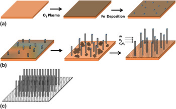
Pillared graphene is a spatial carbon network consisting of CNT pillars grown vertically from large-area graphene sheets. This carbon hybrid structure looks like a building under construction, with CNTs as the pillars and graphene sheets as the floor [Sch. 1(c)]. Scheme 1(a) illustrates the process applied to prepare the growth substrate before the synchronous synthesis. As discussed in Sec. II, Fe particles, “seeds” for CNT growth, were e-beam evaporated on a layer of copper oxide prepared by O2 plasma treatment of copper foil. We first investigate the CVD growth of CNTs on the processed copper substrate and then look into the entire perspective on the synchronous synthesis of the cabin hybrid.
Schematic diagram of (a) preparation of the growth substrate and the catalysts: oxygen plasma treatment of the copper foil followed by iron deposition. (b) Synchronous growth of CNTs and underlying graphene. (c) Pillared graphene hybrid structure comprising vertically grown CNTs as pillars and large-area graphene plane as a floor.

As opposed to copper-based CVD growth of graphene, which is an experimentally established technique,Reference Li, Cai, An, Kim, Nah, Yang, Piner, Velamakanni, Jung, Tutuc, Banerjee, Colombo and Ruoff32, Reference Levendorf, Ruiz-Vargas, Garg and Park33 the synthesis of CNTs on copper surface is challenging due to the undesired interaction between the Cu substrate and the metallic catalysts used for CNTs, such as Fe, Co, and Ni. The main technique utilized to overcome this obstacle is to deposit an intermediate layer between metallic catalysts and Cu surface to act as a separator.Reference Lahiri, Seelaboyina, Hwang, Banerjee and Choi38–Reference Delzeit, Nguyen, Chen, Stevens, Cassell, Han and Meyyappan41 Such barrier layers, however, would restrict the exposure of the copper layer to the flow of carbon source gas that is fundamental in our method.
In our synthesis approach, we aim to implement a temporary separating layer that can be removed or consumed in the course of growth. To address this need, we devise a step of oxygen plasma pretreatment to form a controlled layer of copper oxide on top of copper foil. This oxide layer separates copper from the iron particles that will be subsequently e-beam evaporated [Sch. 1(a)]. Hydrogen flow, introduced at high temperature inside the CVD chamber, could then reduce the copper oxide. Therefore, as the CNT starts growing from the catalysts on the surface of the copper–copper oxide foil, the oxide layer would be gradually reduced back to metallic copper. This finally leads to exposure of the pure copper to acetylene flow (carbon source gas) and the formation of the graphene layer in parallel with the CNTs’ growth [Sch. 1(b)]. This synthesis approach allows us to remove the need for lithography prepatterning of the growth substrate that was a necessary part of previous fabrication approach.Reference Paul, Ghazinejad, Penchev, Lin, Ozkan and Ozkan36
It should be noted that the actual growth system is quite complex and may include additional reactions and products. Based on the ternary Cu–O–Fe phase diagrams, Fe is not thermodynamically stable in the presence of Cu and O. Therefore, extended exposure of iron to copper oxide during long periods of growth will result in the formation of equilibrium phases of Fe–Cu–O compounds such as CuFeO2 and spinal CuFe2O2.Reference Perrot, Arnout and Vrestal42 The fractions of these Fe–Cu–O compounds should be controlled in the CVD growth, as large portions of these compounds may interfere with functionality of the synthesized carbon nanostructure for the envisioned applications such as supercapacitors. We discuss this issue further in detail in the following parts of the discussion.
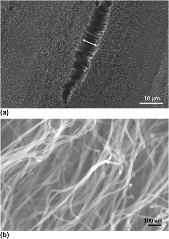
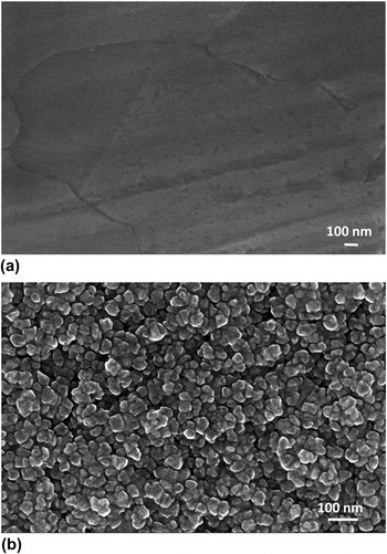
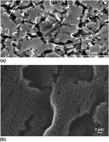
Figure 1(a) displays a typical top view SEM micrograph of a large-area CNT–graphene hybrid layer. The gap in the surface, marked with a double arrow, allows us to see the vertical direction of the CNT growth. This figure also shows the uniform morphology of grown CNTs over the large area of the hybrid film. Figure 1(b) is a higher magnification SEM indicating the average diameter of CNTs to be less than 20 nm with narrow size distribution. To achieve a better understanding of the role of oxide layer in the synthesis, we conducted a comparative study on two similar copper foils, with and without O2 plasma treatment. Figures 2(a) and 2(b) show SEM micrographs of the surfaces of an unmodified and O2 plasma-treated copper foil samples, respectively. Accordingly, Figs. 3(a) and 3(b) show the SEM images of (a) unmodified copper and (b) plasma-treated copper surfaces after deposition of 4 nm iron followed by CVD growth with hydrogen and acetylene. Comparison between Figs. 2(a) and 2(b) suggests that the oxygen plasma treatment dramatically changes the morphology and size of the surface grains. It appears that through conversion of copper to copper oxide, oxygen plasma treatment increases the number of grains and the surface area on the growth substrate. This produces higher level of surface energy, which consequently results in more active nucleation sites for the CNT growth on the surface. According to nucleation and growth theory with higher energy level of the nucleation sites, it is more likely to have higher number of stable embryos on the surface.Reference Askeland and Phule43–Reference Wang, Liu and Kluwer45Figure 3(b) shows SEM image of the same copper foil [Fig. 2(b)] after Fe deposition and CVD process. It is clear that the plasma-treated copper foil substrate gives rise to dense growth of CNTs with vertical alignment, as opposed to unoxidized copper layer. The oxide layer also plays the role of a temporary separator, impeding the unfavorable Fe–Cu interaction by separating two catalyst metals. The unoxidized Cu foil would hardly give rise to any CNTs [Fig. 3(a)]. This could be explained by the increasing interaction between Fe and Cu and the possibility of the formation of metal solid solution due to nanoscale sizes of Fe particles and high growth temperature.Reference Li, Chakrabarti, Schulz and Shanov39, Reference Wang, Liu, Jiang, Ohnuma, Kainuma and Ishida46 Furthermore, the grown CNTs from this substrate would be much larger in diameter and shorter in length as the sparse nucleation sites allow lateral growth of CNTs.
(a) Top view SEM micrograph of CNT pillars in CNT–graphene hybrid, grown on preoxidized copper foil. The image showing dense and vertically aligned growth of CNT pillars on graphene sheet. (b) Higher magnification SEM micrograph of the CNTs.

SEM micrograph of copper substrate (a) before and (b) after O2 plasma treatment.

SEM image of PGN grown on (a) regular and (b) preoxidized copper foil, showing dense and aligned growth of CNT pillars on graphene sheet.

The records of our synthesis attempts suggest that following an accurate procedure, including CVD parameters and copper oxidization specifications, is critical for a viable growth of the CNT–graphene hybrid. In fact, even small violations from optimal conditions could affect the quality of the growth substantially. To understand the roles of the growth parameters, and possibly enhance the window of the growth, we look into the major parameters involved in the growth procedure.
The hydrogen flow and CVD reactor temperature determine the reduction rate of the separating oxide layer. Therefore, a fine balance between the oxide layer thickness and the CVD growth conditions should be observed. Similar to what discussed for hydrocarbons catalytic decomposition, hydrogen molecules dissociate in the presence of metallic catalysts and at the growth temperature of around 750 K.Reference Haluska, Hirscher, Becher, Dettlaff-Weglikowska, Chen and Roth47, Reference Park, Meyer, Roth and Skákalová48 The resulting atomic hydrogen is very reactive, and, in addition to its role in the CVD growth of CNTs, it also acts as a reducing agent for copper oxide layer. A hydrogen exposure will (i) initiate the growth of CNT from iron catalysts that are still separated from copper by the oxide layer. The separation of iron catalyst from underlayer copper is necessary at this step since direct exposure of copper and iron will lead to miscibility of Fe nanoparticles in copper foil, impeding their catalytic function. (ii) It will reduce the oxide separator gradually, allowing the exposure of the metallic copper to hydrogen. This exposure is essential for the simultaneous growth of graphene layers, as the steady CNT growth (mostly by tip growth) continues.
Excessive hydrogen flow rate could be counterproductive as it removes copper oxide layer prematurely and thus reduces iron catalysts activity and lifetime through possible Fe–Cu interaction at some CNT nucleation sites. Additionally, overexposure of iron-deposited copper oxide foil to hydrogen will result in the extended contact between copper oxide, copper, and iron. This, according to ternary Cu–Fe–O phase diagrams,Reference Perrot, Arnout and Vrestal42 increases the formation possibility of the equilibrium Fe–O compounds, such as CuFeO2, which results in reduced performance of the carbon hybrid for different applications such as supercapacitor and field-emission devices. Conversely, underexposure of the growth substrate to hydrogen flow will not effectively reduce the oxide layer and compounds. This inhibits the exposure of metallic copper to the flow of carbon source gas, resulting in incomplete or defective graphene growth.
Based on these limiting factors, viable window of the growth could be enhanced by applying a moderate hydrogen gas flow rate, lower growth temperature (lower bounded by acetylene cracking temperature), and longer growth time. The lower flow rates of hydrogen and carbon gas allow the substrate to maintain the oxide layer over a longer period, enabling steady growth of CNT from the iron catalysts that are temporarily separated from copper. Moderate hydrogen exposure will also extend the time window for the catalytic growth of graphene from a more stable metallic copper. Implementing lower growth temperature will reduce the formation rate of undesired Cu–Fe–O equilibrium compounds that may develop due to longer growth time.Reference Perrot, Arnout and Vrestal42
In catalytic growth of CNTs by CVD, a metallic catalyst particle decomposes the hydrocarbon molecules of a source gas and absorbs carbon atoms to its structure, until it becomes carbon saturated. The absorbed carbon atoms diffuse through the bulk body of the catalyst particle and upon saturation precipitate from the other side to form cylindrically rolled graphene layers.Reference Baker49 Strong catalyst–substrate interaction results in base-growth mode, where catalysts remain on the substrate; and weak catalyst–substrate interaction yields tip-growth mode, in which catalyst remains on the tip of the growing CNT.Reference Baker49, Reference Cassell, Raymakers, Kong and Dai50
The synthesis mechanism for CNT pillars in graphene hybrids is more complicated since it involves the simultaneous growth of graphene and CNTs. In the pillared graphene synthesis, while the CNTs start to grow through the above-mentioned mechanism, copper oxide layer formed by O2 plasma pretreatment is gradually reduced by hydrogen flow until copper atoms resurface and are exposed to acetylene flow in the CVD chamber. Subsequently, the graphene films directly grow on the Cu surface by a surface adsorption mechanism. It is noteworthy that in the copper-based graphene synthesis, graphene is growing by a surface-catalyzed mechanism rather than carbon precipitation process in CVD growth of graphene by nickel.Reference Reina, Jia, Ho, Nezich, Son, Bulovic, Dresselhaus and Kong30–Reference Levendorf, Ruiz-Vargas, Garg and Park33
Considering the overall perspective on the synthesis of pillared graphene, the “floor” graphene grows through carbon nucleation sites. They form by catalytic adsorption of carbon to copper and grow horizontally with the addition of carbon to their boundaries.Reference Li, Cai, An, Kim, Nah, Yang, Piner, Velamakanni, Jung, Tutuc, Banerjee, Colombo and Ruoff32, Reference Levendorf, Ruiz-Vargas, Garg and Park33 The graphene nucleation sites continue expanding by adsorption of more decomposed carbon atoms to their edges, until graphene domains join and form a graphene sheet.Reference Li, Cai, An, Kim, Nah, Yang, Piner, Velamakanni, Jung, Tutuc, Banerjee, Colombo and Ruoff32 In the meantime, the growing planar graphene islands join cylindrically rolled graphene layers, CNTs, at their interface with the substrate, developing PGN. The copper-based graphene growth also allows a more time flexible exposure of the metallic catalyst to carbon source gas. This is crucial to our synchronous fabrication, as we require simultaneous growth of graphene and CNTs for pillared graphene hybrid. Using a copper layer catalyst also yields more uniform graphene with fewer layers.Reference Li, Cai, An, Kim, Nah, Yang, Piner, Velamakanni, Jung, Tutuc, Banerjee, Colombo and Ruoff32, Reference Levendorf, Ruiz-Vargas, Garg and Park33
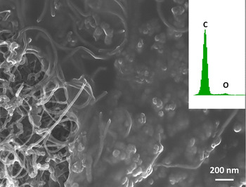
Further study of the synthesized pillared graphene provides a deeper insight into growth mechanism of carbon hybrids. Figure 4 provides an interesting view of the “backside” of a synthesized graphene–CNT hybrid. To obtain this bottom view image, the grown hybrid film was peeled using a double-sided carbon tape and then placed onto SEM sample holder. The image displays how CNTs roots are embedded in graphene sheets. This is an important observation that further indicates the cohesion of the hybrid pillared graphene architecture where CNT “pillars” are connected to graphene “floor.” The EDS spectra taken from the backside of the sample verify carbon as the “floor” material. The SEM image and the fact that carbon tape peeled the CNT–graphene hybrid film rather than only CNTs indicate a robust mechanical connection between synchronously synthesized CNTs and graphene. The back view image also shows a network of intertwining CNTs with several junctions over the interface between graphene and CNTs. These junctions are possibly due to the interaction of Fe–Cu–O fractions in catalytic particles. Large portions of Fe–Cu–O in catalytic layer could affect the performance of CNT–graphene hybrids in application that strongly depends on the composition of the implemented hybrid nanostructure. As discussed in fabrication procedure, thoughtful selection of growth parameters, such growth temperature and hydrogen flow, will allow us to limit the CuO–Fe reactions.
Bottom view SEM micrograph of the backside of the peeled PGN film, showing the graphene film embedding CNT pillars roots.

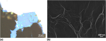
Figure 5(a) displays an optical micrograph of a pillared graphene sample transferred onto SiO2/Si substrate. To remove the pillared graphene structure from copper foil, the underneath Cu attachment was etched using 1 M aqueous FeCl3 solution. Subsequently, the PGN sample was cleaned by HCl solution/DI water and then collected by the SiO2/Si substrate.
(a) Optical micrograph of PGN structure. Partial growth of CNTs reveals graphene underlying film and shows the PGN structure. (b) High magnification SEM micrograph of graphene film in graphene–CNT hybrid.

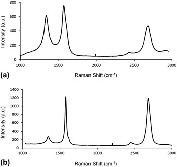
The optical micrograph was taken of a selected area of PGN that is partially covered by as-grown CNTs (due to scarce to zero presence of Fe catalysts), and thus, it reveals the underlying graphene sheet, blue area, under the CNTs. Figure 5(b) shows the SEM image of the graphene layer in the same PGN sample. As it is expected, the graphene layer contains wrinkles, which are mainly caused by mismatch in the thermal expansion coefficient between copper and graphene.Reference Li, Cai, An, Kim, Nah, Yang, Piner, Velamakanni, Jung, Tutuc, Banerjee, Colombo and Ruoff32 A typical Raman spectrum taken from CNTs in the pillared graphene is shown in Fig. 6(a). The G band, centered on 1570 cm−1, is the first-order Raman mode induced by in-plane vibration of carbon atoms in sp 2 hybridized graphene sheets. As a result, the intensity and sharpness of G band are signifying the presence of crystalline graphitic phase in the synthesized material. The D band at 1335 cm−1 is the defect originated second-order Raman band, which indicates the level of defects in graphitic sp 2 structures. The nature of this band is related to one-phonon elastic scattering and it is interpreted as a measure for sp 3 bonds and structural disorders. Thus, the ratio of D band and G band peak intensities, I D/I G, is commonly agreed as a gauge of the quality of CNTs and in general all graphitic materials. The lower values of this ratio show the superior grade of carbon structure and fewer amounts of amorphous carbon disorders and defects. The average value of this ratio taken from our samples is 0.82, which is lower than the values reported from similar studies on the CVD-grown CNTs on copper substrates and our previous reports on PGN synthesis.Reference Paul, Ghazinejad, Penchev, Lin, Ozkan and Ozkan36–Reference Li, Chakrabarti, Schulz and Shanov39, Reference Delzeit, Nguyen, Chen, Stevens, Cassell, Han and Meyyappan41 The higher quality of PGN structure compared to regular CNTs grown on copper substrate may be explained by the different strategies adopted for the synthesis and in particular the effect of intermediate layers.Reference Lahiri, Seelaboyina, Hwang, Banerjee and Choi38, Reference Li, Chakrabarti, Schulz and Shanov39 While we oxidized a thin layer of copper substrate itself to serve as a temporary separating layer, the general approach is to deposit an external intermediate layer as a barrier film on the copper substrate before the CNT growth. The value of I D/I G for our hybrid CNTs is also very close to those reported for multiwalled CNTs that are CVD grown on silicon wafer with iron particles as catalyst and acetylene as the carbon source gas.Reference Sveningsson, Morjan, Nerushev, Sato, Bäckström, Campbell and Rohmund51 This ratio, however, is higher than the ratio obtained from CVD growth by decomposition of methane at around 1000 °C on iron particle, suggesting better crystalline quality in methane-grown CNTs.Reference Li, Zhang, Tao, Xu, Huang, Luo, Luo, Li, Liu, Bao and Geise52 This may be due to intrinsic difference between methane and acetylene precursors and higher decomposition temperature required for CVD growth with methane.Reference Li, Zhang, Tao, Xu, Huang, Luo, Luo, Li, Liu, Bao and Geise52 The Raman spectra did not show any appreciable radial breathing mode peak, which indicates that grown CNTs are mostly multiwalled. Figure 6(b) is a Raman spectrum of graphene sheet in PGN sample. The spectrum, collected from areas with no CNT pillars, confirms few-layer graphene as the “floor” material of the hybrid structure.
(a) Typical Raman spectra of PGN showing the presence of D, G, and 2D band centered around 1335, 1570, and 2672 cm−1, respectively (Thermo Fisher DXR micro-Raman, λlaser= 532 nm). (b) Raman spectra of the graphene sheet in PGN film grown on copper foil.

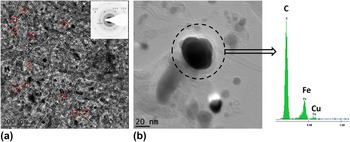
Figure 7 shows a TEM image the of pillared graphene film synthesized from deposited copper layer. To prepare TEM sample, first, the graphene–CNT film was etched from copper using ferric chloride and hydrochloric solutions. The suspended hybrid film is then collected from DI water by a suitable copper grid. The TEM image shows the graphene–CNT hybrid through the underlying graphene. This is a very informative image allowing us to look into the interface between CNT pillars and graphene floor of the carbon hybrid. First, the recurring circular hollow patterns in the interface of a CNT and graphene layer, shown with red circle marks, confirm that CNTs’ roots are embedded in the graphene sheet. This further indicates the smooth transition between the two carbon allotropes, graphene and CNTs, in the hybrid structure.
(a) TEM micrograph of pillared graphene bottom view displaying CNTs roots at their interfaces with graphene film and their tips; inset shows selected area electron diffraction pattern taken from pillared graphene. (b) Typical EDS spectrum taken from a catalyst particle at CNTs tips (dashed circle).

The energy dispersive spectrum (EDS) collected over the area around the dark spots at the tips of CNTs verifies the presence of Fe as the primary composition in catalyst particles. The presence of the Cu peak in EDS is possibly due to the presence of Fe–Cu–O compounds in the catalyst particles. This indicates the likelihood of copper oxide–iron reaction during the growth. The high number of catalyst particles at the tips of nanotubes suggests the synthesis mechanism of CNTs to be tip growth, which points to a low level of the interaction between substrate surface and CNTs catalyst particles. The inset selected area diffraction pattern, taken from sparsely grown CNTs area of pillared graphene, shows concentric circles. This is expected because multiwall CNTs are concentric tubes of cylindrically rolled graphene layers; therefore, we have overlapping sp 2 carbon planes of random orientation with respect to incident electron beam. Furthermore, the typical 6-fold symmetry in diffraction spots supports the presence of mono- to few-layer underlying graphene film.Reference Reina, Jia, Ho, Nezich, Son, Bulovic, Dresselhaus and Kong30, Reference Meyer, Geim, Katsnelson, Novoselov, Booth and Roth53, Reference Meyer, Geim, Katsnelson, Novoselov, Obergfell, Roth, Girit and Zettl54
IV. DEMONSTRATION OF PGN-BASED SUPERCAPACITOR CELLS
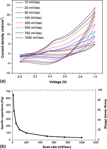
To demonstrate the potential of the carbon hybrid for energy storage, we utilize the synthesized PGN as supercapacitor electrode. The supercapacitor cells were prepared from as-grown PGN films as described in Sec. II. A two-electrode measurement was then used for the electrochemical assessment, where the pretreated two PGN electrodes were assembled into a split flat cell with the as-soaked porous membrane working as a separator in between. The measurements of cyclic voltammetry (CV) were conducted to show the performance of the supercapacitor. The CV scans were performed between 0 and 1 V in 6 M KOH aqueous solution [Figs. 8(a) and 8(b)].
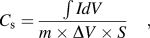
All CV curves show identical behavior. The specific capacitance can be calculated from the curve by using the Eq. (1):
 $$C_{\rm{s}} = {{\int {IdV} } \over {m \times \Delta V \times S}}\quad,$$
(a) CV curves of supercapacitor based on HNO3 acid-treated PGN films. The weight of one PGN film is around 200 μg/cm2. Electrolyte: 6 M KOH aqueous. (b) Specific capacitance and energy density versus scan rates.

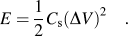
where C s is the specific capacitance, ∫IdV is the integrated area of the CV curve, m is the mass of the active materials, ΔV is the potential range, and S is the scan rate. We carried out the measurements on samples after HNO3 aqueous treatment (HNO3:DI water = 1:4). The specific capacitance of 655, 420, 154, 102, 55, and 40 F/g were obtained for the sweep rates of 10, 20, 100, 200, 500, and 1000 mV/s, respectively [Fig. 8(a)]. Highest specific capacitance of 655 F/g, achieved at a scan rate of 10 mV/s, suggests that the as-prepared supercapacitor cell has good performance.Reference Futaba, Hata, Yamada, Hiraoka, Hayamizu, Kakudate, Tanaike, Hatori, Yumura and Iijima55 Nitric acid treatment can etch Fe-based catalyst and oxides away and at the same time enhances the surface wettability of the carbon hybrid.Reference Lin, Zhong, Bao, Reiber-Kyle and Wang37 Therefore, the surface area increases by end tip opening of CNTs, which further increases the specific capacitance [Figs. 8(a) and 8(b)]. Recent research has shown that activated surface of the carbon material will have higher capacitance, which provides opportunity to increase the performance of the carbon-based storage devices.Reference Zhu, Murali, Stoller, Ganesh, Cai, Ferreira, Pirkle, Wallace, Cychosz, Thommes, Su, Stach and Ruoff56 Moreover, adjusting the growth parameters to reduce the fractions of copper oxide and Fe–Cu–O compounds will improve the storage performance through more effective removal of the catalysts residues from the carbon nanostructure. The energy density was calculated by using Eq. (2):
 $$E = & {1 \over 2}C_{\rm{s}} (\Delta V)^2 \quad.$$
The energy density increases from 10.05 to 91 Wh/kg (for 10 mV/s) after acid treatment, demonstrating a good performance of the PGN supercapacitor comparable to those of carbon-based supercapacitors.Reference Yu, Roes, Davies and Chen57, Reference Hu, Choi, Yang, Jeong, La Mantia, Cui and Cui58
V. CONCLUSION
Large and uniform pillared graphene films were successfully synthesized via simultaneous CVD growth of graphene layers and CNTs on copper foil. The introduced graphene–CNT hybrid is a remarkable carbon nanostructure with tuneable nanoarchitectonics, which is central to application-oriented design of hierarchical graphene structures. The unique mechanism of synchronized CVD growth of CNT and graphene contributed significantly to the composure of the final carbon structure. Detailed characterization of synthesized pillared graphene shows the cohesive structure and robust contact between the two carbon allotropes in the hybrid. Through its tuneable spatial geometry and attractive material properties, this carbon hybrid shows very promising potential for integration into nanoelectronics, energy storage, and thermal management. The direct growth of PGN on copper foil, a significant technical improvement, opens the door for realistic applications of PGN in which it is necessary to have a mechanically flexible and electrically/thermally conductive substrate. As an immediate proof for the functionality of the refined graphene hybrid structure, it has been readily used in a supercapacitor cell. The measurement of the supercapacitor cell demonstrates relatively high energy density with good cycling stability that paves the way for developing future higher energy storage devices.
The present work is also innovative for its synchronous approach to synthesis of multicomponent hybrids. The introduced fabrication methodology is based on premeditated design of catalysts foundation, analysis of carbon formation mechanisms, and thoughtful timing in the fabrication procedure, as synchronization in the growth process is vital. Accordingly, chemical nature, morphology, and organization of the catalysts, as well as preprocessing of the growth substrate, are the key designing measures of this approach. The synchronous parallel growth method offers a practical high-volume production technique for carbon hybrids. It also does not involve any unconventional laboratory style step and is compatible with industrial thin-film fabrication technologies.
Supplementary Material
Supplementary materials can be viewed in this issue of the Journal of Materials Research by visiting http://journals.cambridge.org/jmr.
ACKNOWLEDGMENTS
We gratefully acknowledge funding for this work by the CMMI Division of the National Science Foundation (Award No. 0800680), the Materials Research Science and Engineering Center (NSF-MRSEC) on Polymers (Award No. 0213695), the Nanoscale Science and Engineering Center (NSF-NSEC) on hierarchical manufacturing (Award No. 0531171), and the University of California, Riverside. First author (M.G.) also acknowledges the American Public Power Association DEED fellowship program.