I. INTRODUCTION
Polycrystalline SixGe1–x alloys are crucial in many advanced technologies such as high efficiency solar cells and thin-film transistors for applications in flat panel displays.Reference Eisele, Berger, Nerding, Strunk and Nebel1–Reference Zhao, Meng, Wong and Kwok4 SixGe1–x thin films prepared by physical vapor deposition or chemical vapor deposition at low temperatures are usually in a low-performance, amorphous state. Solid phase crystallization of pure amorphous a-SixGe1–x (a-SixGe1–x) alloys would require very high temperatures in the range of 450–670 °C depending on the a-SixGe1–x alloy composition.Reference Yamaguchi, Sugii, Park, Nakagawa and Miyao5 However, by using a metal contact layer, the crystallization of a-SixGe1–x alloys may be induced at very low temperatures through a process termed metal-induced crystallization (MIC),Reference Wang, Juergens, Wang and Mittemeijer6 which enables the use of low-cost substrates such as plastics. The MIC process significantly differs from the homogeneous crystallization of amorphous semiconductors or the heterogeneous crystallization of amorphous semiconductors at the interface with an insulator substrate.Reference Spinella, Lombardo and Priolo7 After complete crystallization, the unwanted metal phase can routinely be removed either by selective chemical etching or by mechanical polishing. Among other metals, Au and Al lower the crystallization temperature of amorphous Si (a-Si) and amorphous Ge (a-Ge) the most,Reference Wang, Juergens, Wang and Mittemeijer6,Reference Knaepen, Detavernier, Van-Meirhaeghe, Sweet and Lavoie8,Reference Knaepen, Gaudet, Detavernier, Van-Meirhaeghe and Sweet9 and therefore the comparably cheap Al is the most promising metal to be applied for such MIC processes.
Thus, Al-induced crystallization (AIC) of a-SixGe1–x alloys has attracted significant interest in recent years.Reference Gjukic, Buschbeck, Lechner and Stutzmann10–Reference Zhang, Ma, Zhang, Ma and Xu17 However, a fundamental understanding of the process has not been reached yet. Most of the research until now has focused on the AIC of a-SixGe1–x alloys at temperatures close to the Al–Ge eutectic temperature of 420 °C.Reference Gjukic, Buschbeck, Lechner and Stutzmann10–Reference Kurosawa, Kawabata, Sadoh and Miyao16 Hence, to understand the crystallization process from its initiation at about 150 °C, investigation of the nucleation of crystallization at low temperatures appears timely, in particular also because the preferred nucleation sites of the crystalline SixGe1–x (c-SixGe1–x) phase within bilayers of Al/a-SixGe1–x may sensitively depend on the composition of the a-SixGe1–x alloys, since distinctly different AIC behaviors have been observed for Al/a-Ge and Al/a-Si bilayers.Reference Wang, Wang, Jeurgens and Mittemeijer18 In the Al/a-Ge bilayer structure, nucleation of c-Ge takes place both at the interface with Al and at the Al grain boundaries (GBs),Reference Wang, Wang, Jeurgens and Mittemeijer18–Reference Katsuki, Hanafusa, Yonemura, Koyama and Doi20 whereas in the Al/a-Si bilayer structure, nucleation of crystalline Si occurs exclusively at the Al GBs.Reference Wang, Wang, Jeurgens and Mittemeijer18,Reference Konno and Sinclair21–Reference Wang, Gu, Phillipp, Wang, Jeurgens and Mittemeijer23 In the present project, the AIC process of a-SixGe1–x alloys has been investigated for compositions over the whole range of the isomorphous Si–Ge system at low temperatures from 150 to 300 °C and a quantitative thermodynamic model of the AIC process has been developed by evaluation of the interface energies and crystallization energies within the Al/a-SixGe1–x as a function of temperature and alloy composition x.
II. EXPERIMENTAL PROCEDURES
50-nm Al/100-nm a-SixGe1–x bilayer specimens were prepared either by thermal evaporation in a multisource ultrahigh vacuum molecular beam epitaxy system (base pressure of 2 × 10⁻⁸ Pa) or by magnetron sputtering deposition in a triple-source high vacuum chamber (base pressure of 5 × 10⁻⁶ Pa). The 100-nm amorphous SixGe1–x sublayers were deposited on a 50-nm a-Si3N4/50-nm a-SiO2/Si100 substrate by thermal co-evaporation of pure Si and pure Ge using high-temperature effusion cells or by co-sputtering of pure Si and pure Ge targets at an Ar pressure of 3.5 Pa (in both cases Si and Ge purities >99.999 wt%). Without breaking the vacuum, the a-SixGe1–x alloys were then coated with a 50-nm crystalline Al overlayer (Al purity >99.9995 wt%) by thermal evaporation or magnetron sputtering. In this project, identical AIC behaviors were observed regardless of which the above preparation methods were applied. The composition of the a-SixGe1–x alloy thin films was determined by x-ray photoelectron spectroscopy (XPS) measurements of the Si 2p and Ge 3d core levels in a Thermo VG Thetaprobe system using Al-K radiation with a photon energy of 1486.7 eV, after etching off the Al overlayer in 18% HCl and further removing the surface oxide layer by sputtering with 1 keV Ar+ ions in the XPS chamber.
The crystallization kinetics of a-SixGe1–x alloys in the Al/a-SixGe1–x specimens were studied by in situ heating XRD in a Bruker D8 diffractometer equipped with a Cu Kα x-ray source utilizing parallel beam geometry and a heating/cooling stage which was calibrated as described in Ref. Reference Wohlschlogel, Welzel, Maier and Mittemeijer24. The specimens were annealed under a vacuum of 1 Pa at temperatures from room temperature up to a maximum temperature of 300 °C in steps of 25 °C. At each temperature step, the specimens were annealed for 30 min. XRD θ–2θ scans of the SixGe1–x 111 diffraction peak were acquired during the last 15 min of annealing at each temperature.
Auger electron spectroscopy (AES) concentration–depth profiles of the annealed Al/a-SixGe1–x specimens were recorded in a JEOL JAMP-7830F scanning Auger microscope. Using a primary electron energy of 10 keV, the concentration–depth profiles of the specimens were measured by sputtering with 2 keV Ar+ ions in a discontinuous mode. The sputtered and analyzed areas were 100 × 100 µm2 and 10 × 10 µm2, respectively. The peak-to-peak heights of the differentiated AES spectra of Al KLL, Si KLL, and Ge LMM, recorded as a function of sputtering depth, were quantified by applying experimentally determined sensitivity factors.
III. RESULTS AND DISCUSSION
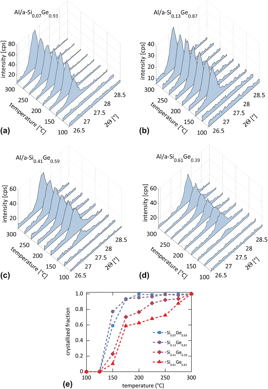
The measured XRD patterns during in situ heating of the Al/a-Si0.07Ge0.93 and Al/a-Si0.13Ge0.87 specimens indicate that the crystallization initiates at 150 °C for both specimens [Figs. 1(a) and 1(b)]. Both specimens had become fully crystallized after annealing at 200 °C, since no further increase in the SixGe1–x 111 diffraction peaks was observed upon continued annealing. In contrast with these results, for the Al/a-Si0.41Ge0.59 and Al/a-Si0.61Ge0.39 specimens only weak SixGe1–x 111 diffraction peaks emerge at 150 °C [Figs. 1(c) and 1(d)]. The subsequent gradual increase of these diffraction peaks upon continued heating from 175 to 300 °C suggests that the crystallization of the a-Si0.41Ge0.59 and a-Si0.61Ge0.39 alloys proceeds gradually upon increasing temperature. Only a single, relatively sharp (full width at half maximum <0.4° 2θ) SixGe1–x 111 diffraction peak, not suggesting any compositional broadening,Reference Mittemeijer and Delhez25,Reference Leineweber and Mittemeijer26 is observed for all Al/a-SixGe1–x specimens during in situ heating. Therefore, it follows that a single and homogeneous crystalline SixGe1–x (c-SixGe1–x) phase develops upon AIC, which is also confirmed by AES concentration–depth profiles as discussed below.
Evolution of the SixGe1–x 111 diffraction peaks upon in situ annealing of the (a) Al/a-Si0.07Ge0.93, (b) Al/a-Si0.13Ge0.87, (c) Al/a-Si0.41Ge0.59, and (d) Al/a-Si0.61Ge0.39 specimens in steps of 25 °C up to a maximum temperature of 300 °C. While the a-Si0.07Ge0.93 and a-Si0.13Ge0.87 specimens are fully crystallized at 200 °C, the crystallization of the a-Si0.41Ge0.59 and a-Si0.61Ge0.39 specimens proceeds gradually up to 300 °C. (e) The crystallized fraction of the a-SixGe1–x alloys as a function of annealing temperature as evaluated from the integrated intensities of the SixGe1–x 111 diffraction peaks [see Figs. 1(a–d)]. Al/a-SixGe1–x specimens of high Si concentration (>41 at.%) crystallize gradually as compared to the very fast (“explosively”) crystallizing a-Si0.07Ge0.93 and a-Si0.13Ge0.87 specimens of low Si content.

The evolution of the volume fraction of crystallized SixGe1–x as a function of annealing temperature was assessed from the evolution of the integrated intensity of the SixGe1–x 111 (x = 0.07, 0.13, 0.41, and 0.61) diffraction peaks in Figs. 1(a)–1(d). To this end, the SixGe1–x 111 diffraction peak area obtained at each annealing step was divided by the peak area obtained at 300 °C (corresponding to full crystallization of all specimens). The thus obtained transformation curves in Fig. 1(e) show that the a-Si0.07Ge0.93 and a-Si0.13Ge0.87 specimens “explosively” crystallize to about 60–80% immediately after the onset of AIC at 150 °C and the crystallization attains completion very fast at 200 °C. In contrast, a remarkably small fraction of only 10–20% crystallization occurs for the a-Si0.41Ge0.61 and a-Si0.61Ge0.39 specimens at the onset of AIC at 150 °C and subsequently the crystallization proceeds only gradually upon continued heating up to 300 °C. Hence, the AIC rate becomes pronouncedly retarded for increasing Si content in the a-SixGe1–x alloy.
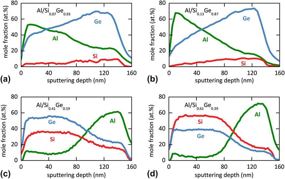
The AES concentration–depth profiles of the Al/a-Si0.07Ge0.93 and Al/a-Si0.13Ge0.87 specimens after full crystallization, i.e., at 200 °C, are shown in Figs. 2(a) and 2(b). For both specimens, the initial Al top layer has only partly intermixed with the initial a-SixGe1–x bottom layer, and the original sublayer sequence is preserved. This is in striking contrast with the AES concentration–depth profiles of the Al/Si0.41Ge0.59 and Al/–Si0.61Ge0.39 specimens after full crystallization, i.e., at 300 °C, shown in Figs. 2(c) and 2(d). For these specimens, the Al sublayer is now located at the bottom while the top layer now practically consists of pure c-SixGe1–x. Hence, during the AIC process in these relatively Si-rich specimens, a complete layer exchange of the Al and SixGe1–x sublayers has occurred.
(a,b) AES concentration–depth profiles of the (a) Al/a-Si0.07Ge0.93 and (b) Al/a-Si0.13Ge0.87 specimens after full crystallization at 200 °C. Only minor intermixing of the Al and SixGe1–x sublayers has occurred. (c,d) AES concentration–depth profiles of the (c) Al/Si0.41Ge0.59 and (d) Al/Si0.61Ge0.39 specimens after full crystallization at 300 °C. A complete layer exchange of the Al and SixGe1–x sublayers has occurred.

The observed constant Si/Ge ratio throughout the depth of the annealed Al/a-SixGe1–x bilayer specimens in the AES concentration–depth profiles in Fig. 2 indicates the formation of a homogeneous c-SixGe1–x phase upon AIC for all the Al/a-SixGe1–x specimens, supporting the above discussion of the XRD results.
Very fast crystallization as observed here for the Al/a-Si0.07Ge0.93 and Al/a-Si0.13Ge0.87 specimens was recently observed for pure a-Ge layers in contact with Al.Reference Wang, Wang, Jeurgens and Mittemeijer18,Reference Wang, Wang, Jeurgens and Mittemeijer27 In that case, full crystallization was realized without layer exchange of the Al and Ge sublayers. The gradual crystallization and the complete layer exchange of the Al/a-Si0.41Ge0.59 and Al/a-Si0.61Ge0.39 specimens are, instead, comparable with the slow crystallization rate of a-Si in Al/a-Si bilayers and the complete layer exchange of the Al and Si sublayers upon full crystallization of a-Si.Reference Wang, Wang, Jeurgens and Mittemeijer18,Reference He, Wang and Mittemeijer28–Reference Wang, Gu, Jeurgens, Phillipp and Mittemeijer30 It is concluded that AIC of a-SixGe1–x alloys, depending on the Si content, complies with two distinct types of crystallization behaviors; the transition between the two types of AIC behaviors occurs between 13 at.% Si and 41 at.% Si.
A metal layer such as Al in direct contact with semiconductors as Si and Ge weakens the covalent bonds between the Si and Ge atoms at the interface with the metal through electronic interaction and thus the mobility of these interfacial Si and Ge atoms is enhanced.Reference Hiraki31 Upon annealing a bilayer structure such as Al/a-Si at 120 °C and above, the semiconductor may diffuse into the Al GBs and form an amorphous wetting layer at the GBsReference Wang, Gu, Phillipp, Wang, Jeurgens and Mittemeijer23 (a process referred to as GB wetting). The amorphous modification of a semiconductor is generally unstable, as compared to the crystalline modification, due to its higher bulk Gibbs energy. However, crystallization of a thin amorphous semiconductor layer at the metal/semiconductor interface or at the GBs can thermodynamically be impeded because a resulting crystalline/crystalline interface generally possesses a higher Gibbs energy than the corresponding amorphous/crystalline interface.Reference Benedictus, Bottger and Mittemeijer32,Reference Jeurgens, Wang and Mittemeijer33 The amorphous layer is thus stable up to a critical thickness, beyond which the lower Gibbs energy of the bulk crystalline phase compensates for the higher interface energies of the newly formed crystalline/crystalline interfaces. The relatively high mobility of the semiconductor atoms at the interfaces (due to the bond-weakening effect) then facilitates the kinetics of this crystallization at such low temperatures (see below) when the crystallization becomes possible thermodynamically.
For the Al/a-Si bilayer system, when the thin a-Si wetting layer at the Al GBs exceeds a critical thickness  $h_{{\rm{GB}}}^{{\rm{crit}}}$, the release in Gibbs energy upon crystallization (−ΔG cryst) may compensate for the increase in interface energies. The critical thickness
 $h_{{\rm{GB}}}^{{\rm{crit}}}$ for crystallization of the a-Si wetting layer at the Al GBs is determined byReference Wang, He, Zhao and Mittemeijer22
 $$- \Delta {G_{{\rm{cryst}}}} \cdot h_{{\rm{GB}}}^{{\rm{crit}}} = 2\left( {\gamma _{{\rm{c - Al/c - Si}}}^{{\mathop{\rm int}} } - \gamma _{{\rm{c - Al/a - Si}}}^{{\mathop{\rm int}} }} \right)\quad,$$
where the interface energies of the initial c-Al/a-Si and newly formed c-Al/c-Si interfaces are denoted by  $\gamma _{{\rm{c - Al}}/{\rm{a - Si}}}^{{\rm{int}}}$ and
 $\gamma _{{\rm{c - Al}}/{\rm{c - Si}}}^{{\rm{int}}}$, respectively. Similarly, the critical thickness
 $h_{{\rm{int}}}^{{\rm{crit}}}$ for crystallization of the bond-weakened a-Si layer at the Al/a-Si interface is determined byReference Wang, He, Zhao and Mittemeijer22:
 $$- \Delta {G_{{\rm{cryst}}}} \cdot h_{{\mathop{\rm int}} }^{{\rm{crit}}} = \gamma _{{\rm{c - Al/c - Si}}}^{{\rm{int}}} + \gamma _{{\rm{c - Si/a - Si}}}^{{\mathop{\rm int}} } - \gamma _{{\rm{c - Al/a - Si}}}^{{\mathop{\rm int}} }\quad.$$
In this case, upon crystallization two new interfaces c-Al/c-Si and c-Si/a-Si are created with the corresponding interface energies denoted by  $\gamma _{{\rm{c - Al}}/{\rm{c - Si}}}^{{\rm{int}}}$ and
 $\gamma _{{\rm{c - Si}}/{\rm{a - Si}}}^{{\rm{int}}}$, respectively. Similar calculations can also be applied for the c-Al/a-Ge bilayer system. To calculate the energetics for crystallization of a-SixGe1–x alloys in Al/a-SixGe1–x bilayer structures, it is necessary to assess the c-Al/a-SixGe1–x, c-Al/c-SixGe1–x, c-SixGe1–x/a-SixGe1–x interface energies and the SixGe1–x crystallization energies, for SixGe1–x alloys of different compositions. Considering the structural similarity of c-Si and c-Ge and also of a-Si and a-Ge, a linear dependence of the interface energies and the crystallization energy on the SixGe1–x alloy composition x is adopted.
The critical thicknesses for the crystallization of pure a-Si, a-Si0.41Ge0.59 alloy and pure a-Ge at Al GBs and at the interface with Al are calculated based on Eqs. (1) and (2) for crystallization of pure a-Si and analogous equations for crystallization of a-Si0.41Ge0.59 alloy and pure a-Ge. To this end, the thickness of 1 monolayer (ML) of SixGe1–x is estimated by linear interpolation of the thicknesses of 1 ML of pure Si and 1 ML of pure Ge, of 2.2 Å and 2.5 Å, respectivelyReference Slater34; the thickness of the bond-weakened layers of Si and Ge atoms at the interface with c-Al is estimated to be about 2 ML.Reference Wang, Wang, Jeurgens and Mittemeijer18,Reference Hiraki31 Recognizing that the semiconductor wetting layer at the Al GBs is sandwiched between two Al grains, the maximum thickness of bond-weakened semiconductor atoms here is about 4 ML.Reference Wang, Wang, Jeurgens and Mittemeijer18
On this basis, the calculated critical thicknesses for the crystallization of pure a-Si, a-Si0.41Ge0.59 alloy and pure a-Ge at Al GBs and at the interface with Al, in units of ML, are shown as a function of temperature by the red, purple, and blue, respectively, solid and dashed lines in Fig. 3(a). The layer thicknesses of the bond-weakened semiconductor atoms at Al GBs and at the interface with Al are indicated in Fig. 3(a) by the horizontal gray solid and dashed lines, respectively.
(a) Critical thicknesses  $h_{{\rm{GB}}}^{{\rm{crit}}}$ and
 $h_{{\mathop{\rm int}} }^{{\rm{crit}}}$ for nucleation of crystalline Si, Si0.41Ge0.59, and Ge (red, purple, and blue lines) at the Al GBs and at the interfaces with Al as indicated by the solid and dashed lines, respectively. The thicknesses of the bond-weakened a-Si, a-SixGe1–x, and a-Ge layers are about 4 MLs at the Al GBs and about 2 MLs at the interfaces with Al (horizontal gray solid and dashed lines). (b) Critical temperature as a function of SixGe1–x alloy composition above which crystallization of the a-SixGe1–x alloy at the interface and Al GBs is possible. The experimentally determined onset crystallization temperatures of the investigated Al/a-SixGe1–x specimens (x = 0.07, 0.13, 0.41, and 0.61) have been indicated by crosses to visualize whether crystallization upon annealing is expected to proceed very fast without layer exchange (white regime) or gradually in association with complete layer exchange of the Al and SixGe1–x sublayers (shaded regime).

If the critical thickness for crystallization is smaller than the layer thickness of the bond-weakened atoms in the amorphous semiconductor, crystallization of the amorphous semiconductor layer will take place. From Fig. 3(a), it follows that crystallization of pure a-Si at Al GBs may occur at temperatures above 140 °C, whereas crystallization of pure a-Si at the Al/a-Si interface is prohibited up to much higher temperatures. Regarding the Al/a-Ge system, crystallization of pure a-Ge may occur not only at Al GBs, but also at the interface with Al already at temperatures above 50 °C.
Whether a layer exchange upon AIC occurs or not is controlled by the possible crystallization sites of the semiconductor. For an Al/a-Si bilayer specimen, in which nucleation of c-Si is restricted to the Al GBs, a complete layer exchange during AIC is achieved by continuous inward diffusion of Si and growth of c-Si at the Al GBs.Reference Wang, Wang, Jeurgens and Mittemeijer18,Reference Wang, Gu, Jeurgens, Phillipp and Mittemeijer30 In contrast, nucleation of c-Ge in an Al/a-Ge bilayer specimen occurs both at the Al GBs and at the interface with Al. Thereby, the a-Ge has fully crystallized long before layer exchange, by a mechanism as described above for an Al/a-Si bilayer, has been achieved.
According to the present model calculation [Fig. 3(a)], the critical temperature for crystallization of a-Si0.41Ge0.59 at the interface with Al is given by the intercept of the purple dashed  $h_{{\mathop{\rm int}} }^{{\rm{crit}}}$ curve with the gray dashed horizontal line indicating the 2 ML thickness of the bond-weakened SixGe1–x atoms at the interface with Al. The critical temperature for this crystallization of a-Si0.41Ge0.59, at the interface with Al, is as high as 350 °C (compared with the critical temperature of 50 °C for crystallization of pure a-Ge at the Al/a-Ge interface). Below 350 °C, nucleation of a-Si0.41Ge0.59 is restricted to the Al GBs, as is the case for pure a-Si in an Al/a-Si bilayer specimen. Now considering Al/a-SixGe1–x specimens over the entire composition range (0 ≤ x ≤ 1), crystallization of a-SixGe1–x at Al GBs is always possible at low temperatures [<150 °C, see Fig. 3(a)]. However, the calculated critical temperature for nucleation of c-SixGe1–x at the interface with Al, which is given by the intercept of the composition-dependent
 $h_{{\mathop{\rm int}} }^{{\rm{crit}}}$ curve and the gray dashed horizontal line of 2 ML in Fig. 3(a), rises significantly with increasing Si content x: see the calculated result shown in Fig. 3(b).
The presented model predicts the occurrence of nucleation of crystallization of a-SixGe1–x in the Al/a-SixGe1–x system, which is solely governed by interface thermodynamics, independent of annealing time. The shaded area below the curve of the calculated critical temperature in Fig. 3(b) represents those a-SixGe1–x alloys of compositions for which crystallization will exclusively initiate at the Al GBs. Since diffusion of the Si and Ge atoms into the GBs is a thermally activated process, the crystallization for the a-SixGe1–x alloys in this regime occurs in a gradual manner. As discussed above, the continuous inward diffusion and growth of crystalline SixGe1–x at the Al GBs lead to a complete layer exchange after crystallization (see Ref. Reference Wang, Wang and Mittemeijer29). The white area above the curve of the calculated critical temperature in Fig. 3(b) represents those a-SixGe1–x alloys for which crystallization will initiate both at the Al GBs and at the interface with Al. This leads to an “explosive” crystallization for the a-SixGe1–x specimens in this regime. In this case, full crystallization will occur without substantial intermixing of the original Al and SixGe1–x sublayers, i.e., the original layer sequence is largely preserved.
The experimentally determined (almost equal) onset crystallization temperatures of the investigated Al/a-SixGe1–x specimens (x = 0.07, 0.13, 0.41, and 0.61) have been indicated by the crosses in the plot of the critical temperature in Fig. 3(b). In complete agreement with the above presented theoretical model, the a-Si0.07Ge0.93 and a-Si0.13Ge0.87 specimens crystallized very fast upon annealing at 150–200 °C without the occurrence of a layer exchange [white regime in Fig. 3(b)], whereas the a-Si0.41Ge0.59 and a-Si0.61Ge0.39 specimens crystallized only gradually and indeed showed a complete layer exchange after full crystallization [shaded regime in Fig. 3(b)].
For potential applications of polycrystalline SixGe1–x thin films prepared by AIC, e.g., in high-efficiency solar cells and thin-film transistors, it is imperative to achieve large grain sizes and a homogeneous, complete layer exchange of the sublayers. It has been reported that large-grained and homogeneous c-SixGe1–x alloys of high Ge fraction (x < 0.5) are very difficult to obtain without the introduction of an interfacial oxide layer acting as a diffusion barrier to retard the AIC process,Reference Kurosawa, Tsumura, Sadoh and Miyao14,Reference Kurosawa, Sadoh and Miyao15 which would require an additional processing step in a large-scale production. The present model, as validated by the experimental results, on the detailed temperature dependence of the AIC behavior is therefore highly beneficial in selecting the appropriate annealing temperature to realize a slow and gradual crystallization of Ge-rich SixGe1–x thin films, in which a complete and homogeneous layer exchange is realized [the shaded area in Fig. 3(b)].
IV. CONCLUSIONS
The AIC of amorphous SixGe1–x alloys with compositions over the whole range of the isomorphous Si–Ge system (0 ≤ x ≤ 1) exhibits strikingly different behaviors: At low Ge content, the crystallization of a-SixGe1–x occurs gradually in association with exchange of the Al and SixGe1–x sublayers, whereas at high Ge content, the crystallization of a-SixGe1–x proceeds very fast and attains completion without layer exchange. These observations can be understood on the basis of interface thermodynamicsReference Jeurgens, Wang and Mittemeijer33: Crystallization of a-SixGe1–x at the Al GBs may occur for all Al/a-SixGe1–x specimens at low temperatures (<150 °C), but a critical temperature exists for nucleation of crystalline SixGe1–x at the Al/a-SixGe1–x interface. This critical temperature increases pronouncedly with increasing Si content in the initial a-SixGe1–x alloy (from 50 °C for x = 0 to 470 °C for x = 0.5). At temperatures below the critical temperature for interface nucleation, the a-SixGe1–x alloy will exclusively crystallize at the Al GBs and an exchange of the Al and SixGe1–x sublayers upon AIC occurs. Above the critical temperature, the a-SixGe1–x alloy can crystallize also at the interfaces with Al, and as a consequence the crystallization proceeds “explosively” without that layer exchange can take place.
ACKNOWLEDGMENTS
The authors are grateful to Mr. Reinhart Völker for preparation of specimens by magnetron sputtering, to Dipl.-Ing. Bernhard Siegle and Dipl.-Ing. Martin Noah for AES measurements, and to Dipl.-Ing. Gerd Maier for support with in situ XRD measurements.