I. INTRODUCTION
Amorphous silicon (a-Si) thin film is an important semiconductor that has been used in modern microelectronic systems, for example, large glass plates with p-i-n structure for assembly into low-cost solar cells had deposition of a-SiReference Galloni1 and radio frequency identification (RFID) tags contains a-Si thin film transistor (TFTs) as the major active material.Reference Chan, Kirchhoff, Gordijn, Knipp and Stiebig2 These thin films were mainly fabricated using radio-frequency glow discharge reactors, the latter more commonly known as plasma-enhanced chemical vapor deposition (PECVD) systems, where silane was dissociated by the plasma reactions. A large-sized air-shower head allows uniform deposition silicon films of sizes above 1 m2 on glass plates. This explains why these amorphous thin films are the fundamental material for constructing TFT in large-sized liquid crystal displays (LCDs). Owing to the disordered nature of this amorphous semiconductor, low carrier mobility limits the performance of switching time in TFTs.Reference Lin, Sah and Lee3 The consequence is that active-matrix LCDs operate at relatively lower speeds compared to the single crystal silicon–based transistors. In addition, there are disadvantages in using a-Si in photovoltaic applications. For example, hydrogenated amorphous silicon (a-Si:H) solar cells are affected by the formation of metastable defects, which provide recombination of extra electrons and holes when photon generation assesses carriers. Hence, it reduced 20–30% of the cell efficiency.Reference Cabarrocas, Morral, Lebib and Poissant4 As such, the improvement in the material properties is an important issue for the continual commercialization of electronic products.
One key point when comparing both research results and industrial production is the concern in the process temperature, which is related to the production cost. The conventional plasma process requires a temperature of 350 °C or above to achieve the uniform deposition of a-Si films at a deposition rate of 0.1 nm/s. Such a growth condition limits the materials available for deposition, such as flexible plastic substrates. An additional problem in using PECVD at a lower deposition temperature is that it causes the degradation of the film quality, inactivation of dopants, and increase in the surface roughness owing to continuous ion bombardment.
Nanocrystalline silicon has been widely studied in recent years because of its superior electronic properties and its increased stability against prolonged light exposure.Reference Meier, FluÈckiger, Keppner and Shah5 The electron mobility of nanocrystalline silicon is about 10–50 cm2/V s and has a broader absorption range in the visible part of the solar radiation.Reference Xu, Liao, Kong, Zeng, Hu, Diao and Zhang6 Until now, deposition techniques for producing nanocrystalline silicon thin film have focused on the PECVD process by decomposing monosilane or disilane. This process requires the dilution of silane with hydrogen at a relatively high substrate temperature of 350 °C to increase the crystalline volume fraction.Reference Klein, Finger, Carius, Wagner and Stutzmann7–Reference Valipa, Sriraman, Aydil and Maroudas9 Again, there is limitations in the types of substrate that can be used. Moreover, silane gas is flammable and the doping gases are toxic. Thus, a solution to this is growing films from solid silicon.
Vacuum-arc discharge technique is an ideal deposition tool for tetrahedral amorphous carbon thin films.Reference Chua, Teo, Tsai, Milne, Sheeja, Tay and Schneider10 This deposition technique has the advantages of high deposition rate, processing at room temperature, and low cost. Therefore, vacuum arc discharge may be preferred as an alternative method to the conventional PECVD process for fabricating silicon films. Compared with the PECVD process, arc discharge method has three orders of higher magnitude of plasma density, which resulted in a much higher thin film deposition rate.Reference Suzuki, Niino and Katoh11
In this study, we modified the arc discharge system previously used to prepare tetrahedral amorphous carbon thin film and transformed it to produce silicon thin films instead. Plastic substrate was used in our system when the substrate holder was simultaneously cooled using liquid nitrogen so as to prevent melting of the substrate due to plasma heating. Continuous thin film was produced during deposition, and these films were firmly attached to the plastic substrate. We believe that this is the first report on the deposition of doped silicon films on plastic substrate using vacuum-arc discharge technique without any external post implantation or annealing effects.
II. EXPERIMENTAL
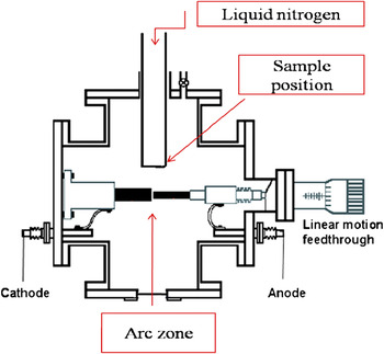
A lab-assembled vacuum-arc discharge system was used in this study. The schematic diagram of the apparatus is shown in Fig. 1. The apparatus had a vacuum chamber (105 × 105 mm2) equipped with a linear feedthrough. The linear motor was used to control the feed-through movement. It maintains a perfect gap between the cathode and anode to discharge the stable plasma. The vacuum arc produces a high temperature and the evaporation of the source material into a plasma jet creates a trajectory to the substrate. Graphite rods were used as an interconnection between the silicon electrodes and the feed-through leads. We used a highly doped single-crystal silicon wafer (0.005 Ω cm) as the electrode, which also acts as the silicon source in the configuration. Coning 7059 slide glass and ULTEM 1000B thermoplastic polyetherimide films from GE (General Electric Company, NY) were used as the substrates. These substrates were subsequently placed on the holder facing down to the arc center. The substrate holder was then filled with liquid nitrogen to quench the substrates to 77 K. The chamber base pressure was evacuated to 3 × 10⁻⁷ Torr and the arc discharge current was set to 30 A. Several samples were then deposited on the glass and plastic plates. The deposition rate of the silicon growth in the vacuum arc discharge system is ∼10 nm/s. All the specimens are approximately 100 nm thick and show good uniformity across the 12 mm diameter (see inset of Fig. 2).
Schematic diagram of lab-assembled vacuum arc system.

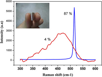
Raman spectra show two different examine points (10 μm apart) that have large differences in crystalline volume fraction. (Inset: silicon film deposited on a plastic substrate).

The Raman spectroscopy with 514.5 nm He–Ne laser was used to observe the structure of the samples and for estimating the crystalline volume fraction (X c). This calculation is based on the ratio of integrated intensity over the relative Raman spectrum peak position, 520 cm−1 for crystalline-phase signal and 480 cm−1 for amorphous-phase signal. A five-point area testing was performed to study the distribution of the crystallinity of the films. A JEOL JEM-2010F field emission transmission electron microscope (TEM; JEOL Ltd., Tokyo, Japan) with a point-to-point resolution of 0.17 nm was used to study the morphology of the films. During the scanning, the electrons were accelerated to 200 kV and a high-angle annular detector was used to collect the electrons that scattered at large angle. A four-point probe was used to measure the sheet resistivity of the specimens. The average values were calculated on the basis of the three readings for each of the sample. The crystallinity of the specimens were studied using a Bruker D8 Advanced Thin Film XRD system, using a Cu Kα (1.542 Å) x-ray source. A scanning step of 0.02° and time of 1 s per step were used. The scanned region was fixed at 20°–70°.
III. RESULTS AND DISCUSSION
First, the microstructure of the film has to be studied. The Raman spectrum is shown in Fig. 2; the crystallinity of the films, X c, can be calculated using the equation from Ref. Reference Bustarret, Hachicha and Brunel12.

where X c is the crystalline volume fraction, I c is the area of the peak from the crystal, and I a is the area of the peak from the disordered silicon called the amorphous phase. The results indicate that, using a microscopy-equipped micro-Raman system, we can find different examination points that are only 10 μm apart from each other and have large differences in crystalline volume fraction X c, ranging from 4 to 87%. It is extraordinary that large variations in crystal fractions over the entire thin film under one deposition zone.
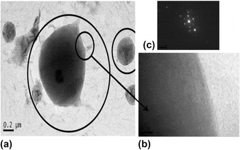
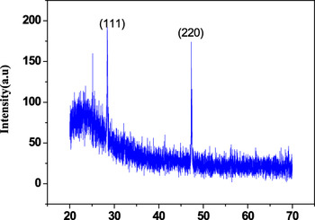
High-resolution transmission electron microscopy was used to analyze the contents of the crystalline volume found in the Raman studies. The TEM images revealed that many crystallite clusters were embedded in an amorphous matrix as shown in Fig. 3. These clusters were spherical in shape and had sizes ranging from 1–4 μm. Using in situ energy-dispersive x-ray spectroscopy and selected-area electron diffraction), it was confirmed that both these particles and the surrounding amorphous matrix were silicon with no other elements detected within 0.1 at.%. The particles are highly crystalline (see inset of Fig. 3). In addition, TEM also showed that these crystallite clusters were randomly distributed throughout the specimen. XRD measurements were also used here as an effective technique for a more quantitative determination of crystallinity. The pattern shown in Fig. 4 indicates the diffraction lines of (111) and (220) clearly, suggesting a considerably high amount of crystalline clusters inside the thin film and oriented along these two directions.
TEM images. (a) Spherical particles embedded in amorphous matrix. (b) These particles are fully crystallized. (c) The electron diffraction pattern shows highly ordered tetrahedral structure of crystalline.

XRD spectrum shows the experimental sample containing crystal orientation along (111) and (220) direction.

The formation of nanocrystallite cluster in a-Si thin film is unusual in a cathodic arc process. In a separate study, there are many reports on the formation of nanocrystalline Si particles in a-Si:H thin films using PECVD technique. There are some differences in these two techniques; for example, in the PECVD process, SiH4 gas source is used, which leads to the formation of different and complex ionic states of Si, H, and SiHx. In the case of the cathodic arc, the arc plasma is generated at the cathode in high vacuum and the ions are pure Si. These Si ions in the arc plasma have been reported to have a distribution of 63% Si ions having +1 charge and 35% Si ions having +2 charges.Reference Anders13 Furthermore, previous reports have confirmed that the cathodic arc deposition process tends to give hydrogen-free films.Reference Cuomo, Pappas, Bruley, Doyle and Saenger14 However, understanding the processes in PECVD may give some insights on the mechanism of a cathodic arc process.
It has been widely reported that PECVD process may give rise to “dusty plasma” depending on the growth conditions, leading to simultaneous nanocluster and/or powder formation. The growth condition can also determine whether these particles are embedded simultaneously in the amorphous hydrogenated thin film. It is widely believed that these particles are formed in the secondary reactions separately before depositing onto the substrates.Reference Cabarrocas, Morral, Lebib and Poissant15 In summary, some of the factors that favor the formation of clusters include the following: (i) increasing the deposition pressure, (ii) modulating the radio frequency source, and (iii) increasing the deposition rate.Reference Valipa, Sriraman, Aydil and Maroudas9, Reference Cabarrocas, Morral, Lebib and Poissant15
In the case of the cathodic arc, there may be some similarities. Although the arc plasma is well known to be a clean plasma (only pure source materials), particles are formed through the by-products of the arcing process, mainly microparticulate droplets. These molten droplets are generated during the striking process.Reference Fallon, Veerasamy, Davis, Robertson, Amaratunga, Milne and Koskinen16 In the field of hard-coatings where the vacuum-cathodic arc process is used to deposit amorphous diamond films for wear protection layer, these microdroplets are usually filtered out using torroidal bend filters, thus resulting in a microdroplet-free film. In this case, the microdroplets are the seed crystals in the formation of nanocrystalline silicon films. Therefore, it is highly possible that all these crystallite clusters have to originate from the source.
As such, when the vacuum arc was ignited, the thermal expansion coupled with the high temperature “exploded” the surface of the electrodes, resulting in the simultaneous release of nanosized silicon particulate droplets and silicon ions from the arc zone. The arcing effect also generates a slightly higher pressure with the base pressure readings at ≈10−4 Torr. The high-pressure plum carries the silicon droplets along with the silicon ions directly into the substrate. The deposition of the silicon ions onto the substrate can be described using the subplantation model of carbon for cathodic vacuum arcs.Reference Robertson17, Reference Lifshitz, Kasi, Rabalais and Eckstein18 This model describes the penetration and incorporation of carbon species in subsurface positions, leading to densification (and stress formation). Although many of these models were used to describe the effect of carbon ions, we believed that these models are also applicable to silicon as the ion energy of silicon ions have been reported to be ∼18 eV, similar to that of carbon ions at 20 eV.Reference Bilek, Chhowalla, Weiler and Milne19 Subsequently, this will lead to the formation of highly dense a-Si films. The usage of the subplantation for silicon was supported on the basis of our experimental evidence confirming the presence of stress/strain in the deposited films. The peak position measured from Raman spectra was shifted downwards, lower than 520 cm−1, indicating that tensile strain was accumulated in our silicon films.Reference Kimura and Katoda20, Reference Paillard, Puech, Laguna, Carles, Kohn and Huisken21 This corroborates with the model predicting the formation of intrinsic stress as widely reported in amorphous carbon films.
By comparison, the ionic energy in the cathodic arc process is still much higher than those reported for radio frequency magnetron sputtering and PECVD processes, thus, indicating that excess energy is present.Reference Suzuki, Niino and Katoh11 Unlike many room temperature deposition processes, the substrate holder in this work is maintained at 77 K, which implied that any heat energy generated during the ion deposition process will be rapidly quenched. This implied that the “thermal spike effect” during ion deposition affecting microstructural bondings in the film may not play a role in this case. The absence of thermal distribution effects (or the reverse, being rapidly quenched) implied that any particulate droplets impinging onto the sample surface will retain its original state. As such, we suspect that the molten silicon droplets ejected from the electrode may be melted only at the topmost shell, while the innermost core may still be a crystalline structure. The travel through vacuum may lead to surface or gradual shell (layer-by-layer) corrosion effect. Further evidence of this was observed in the relationship between substrate position to the crystalline areas on the substrate. The crystalline areas increased when the substrates were placed closer to the arc zone. These results confirmed that when the substrates are close to the arc zone, more liquid droplets will be collected at the substrate. By increasing the substrate-to-arc distance, simply by pulling the substrate holder away from the arc zone, most of the droplets had probably self-corroded and the residual ions pumped away before arriving at the substrate. Compared to the 85% area covered by crystalline structure, when the deposition condition is 4 cm from substrate to arc center, there are no crystalline structure obtained in the entire film when the substrate is placed 35 cm away from the arc zone.
The fast quenching at the substrate surface provided ideal crystal seeds to produce higher crystalline structure locally during the deposition. However, the other areas in which deposition of silicon droplets was absent, the only path for thin film growth has to be an amorphous microstructure from the incoming flux of silicon ions. In general, this results in the formation of an a-Si matrix with nano/micron crystallite particles embedded inside the matrix.
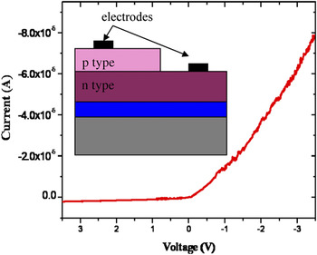
The subplantation of silicon ions into the substrate also implied that good adhesion was obtained. Because both the film and the substrate were silicon, in this case, a good interface was obtained. This good interface was extremely crucial for device fabrication. First, the electrical conductivity was measured using a four-point probe method.Reference Schroder22 The measurements were carried out at room temperature and atmospheric pressure. Results showed that the resistivity of the deposited film was 0.3–0.4 Ω cm. An impurity concentration of 10−17 was correlated from the resistivity value.Reference Sze23 The dopants present in the silicon electrode are simultaneously implanted with the silicon ions into the thin film during growth. Being an amorphous structure, it is highly possible that it does not require any dopant activation. A p-n junction diode was fabricated to demonstrate the ability to do in situ doping using this technique (see inset in Fig. 5). The p-type thin film was deposited on an n-type single crystal silicon wafer with the resistivity of 1–10 Ω cm. The I–V characteristics are shown in Fig. 5, which demonstrates a curve of an ideal diode.
I–V characteristic shows an asymmetric curve similar to an ideal p-n diode. The inset shows the fabricated schematic structure of our diode.

IV. CONCLUSIONS
We successfully deposited nanocrystalline-doped silicon thin films on plastic substrates. The samples were characterized by Raman spectroscopy, and TEM indicates that the mixture structure has nanocrystalline particles embedded in the amorphous structure. We believe that the crystal clusters originate from the source of silicon. The resistivity of the film was 0.3–0.4 Ω cm, and this is due to the dopants transported simultaneously during the deposition process and implanted in situ into the a-Si film. Without any post-deposition annealing process, the silicon thin film can maintain a high conductivity inherited from the dopants originally from the silicon electrodes and a p-n junction diode device has been demonstrated. We have shown that the high crystalline fractions a-Si films are deposited on flexible substrates. This process will be useful for the next generation microelectronics.