I. INTRODUCTION
Transparent conducting oxides (TCOs), such as the predominant thin films of indium-doped tin oxide (ITO), are being used for transparent electrodes (TEs) and anodes in various electronic and optoelectronic devices.Reference Chopra, Major and Pandya1 These include applications in layered structures, such as memory devices,Reference Pan, Gao, Chen, Song and Zeng2 solar cells, light emitting diodes, heat mirrors, electroluminescent, display technologies,Reference Sivaramakrishnan and Alford3 and other devices.Reference Chopra, Major and Pandya1,Reference Pan, Gao, Chen, Song and Zeng2 Zinc oxide (ZnO) is one of the promising transparent semiconducting oxides that is being explored for TE applications in passive and active devices.Reference Hadis and Ümit4
In its pure form, ZnO usually exhibits n-type conductivity.Reference Chopra, Major and Pandya1,Reference Al-Kuhaili, Al-Maghrabi, Durrani and Bakhtiari5,Reference Dhananjay, Nagaraju and Krupenidhi6 It has a high melting point of ∼1975 °CReference Pearton, Norton, Heo and Steiner7 and a large intrinsic band gap energy between ∼3.2 and 3.4 eVReference Sivaramakrishnan and Alford3,Reference Al-Kuhaili, Al-Maghrabi, Durrani and Bakhtiari5,Reference Dhananjay, Nagaraju and Krupenidhi6 at room temperature. This leaves it with high optical transmission in the visible region of the solar spectrum. ZnO also has a high breakdown voltage that enables it to sustain large electric fields, high power, and high temperature operations.Reference Pearton, Norton, Heo and Steiner7 Due to these promising properties, ZnO-based thin films have received considerable attention in the literature.Reference Xudong, Jinhui, Jin and Zhong8–Reference Onodera, Tamaki, Jin and Yamashita12 Hence, research on ZnO thin films goes back many decades.Reference Hadis and Ümit4
The sustained research interest in ZnO has been fueled by its high abundanceReference Song, Aberle and Xia13 and the potential for its applications as a low cost substrate or transparent conducting thin filmsReference Al-Kuhaili, Al-Maghrabi, Durrani and Bakhtiari5 in large area solar cells, light emitting diodes, flat panel displays,Reference Sivaramakrishnan and Alford3 and other optoelectronic devices.Reference Chopra, Major and Pandya1,Reference Hadis and Ümit4 Furthermore, ZnO is also a nontoxic material with flexible hexagonal wurtzite structure. This makes it easy to use ionic substitution and doping to introduce structural phase transformations and conductive charge carriers that make it attractive for a wide range of applications.Reference Chopra, Major and Pandya1,Reference Hadis and Ümit4,Reference Dhananjay, Nagaraju and Krupenidhi6–Reference Lin, Huang and Lii14
However, a significant number of practical challenges must be overcome prior to the widespread use of ZnO. These include the high electrical resistivity of ZnO, which prevents its use in thin films that require TEs with lower sheet resistances, while retaining good optical transmission properties. In an effort to overcome this challenge, a number of research groups have explored the use of n-type doping with group III elementsReference Chopra, Major and Pandya1,Reference Tsujinoa, Hommaa, Tomoaki, Isao and Yoshihiko15 such as aluminum (Al),Reference Aktaruzzaman, Sharma and Mahgotra16 boron,Reference Nakada, Yukiyasu, Naoki and Akio17 indium,Reference Gomez, Maldonado, Asomoza, Zironi, Canetas-Ortega and Palacios-Gomez18 and gallium.Reference Tiburcio-Silver and Avila-Garcia19 These have been used to enhance the electrical conductivity of ZnO thin films.Reference Chopra, Major and Pandya1,Reference Tsujinoa, Hommaa, Tomoaki, Isao and Yoshihiko15 However, single-layer doped TCOs have been shown to have limited chemical and thermal stabilities in various environments.Reference Park, Kim, Rhee, Ko and Shon20 Furthermore, their solar transparencies and electrical conductivities are limited generally by their extremely high ionized impurity scattering phenomena.Reference Sivaramakrishnan and Alford3
In an effort to address some of the challenges above, multilayered ZnO/metal/ZnO composite thin film structures have been proposed for the effective enhancement of the electrical conductivity of ZnO-based thin films.Reference Sivaramakrishnan and Alford3,Reference Sahu, Lin and Huang21 Optimized multilayered ZnO/metal/ZnO films can be designed to have low resistivities that are comparable to those of their highly conductive intermediate metal layers and high visible region solar transparencies that are needed for applications in solar cells and light emitting diodes.Reference Sahu and Huang22 They also have the attractive features of low cost and nontoxicity.Reference Sivaramakrishnan and Alford3 Furthermore, multilayered ZnO/metal/ZnO film sandwiches have been shown to have good TE properties and better durability than single-layer doped ZnO and/or metal films.Reference Sahu, Lin and Huang21–Reference Ando and Miyazaki23
Nevertheless, there are relatively few reports of multilayered ZnO/metal/ZnO composite films.Reference Sahu and Huang22 There is also a need to develop TE material alternatives to ITO-coated TCOs,Reference Sivaramakrishnan and Alford3,Reference Sahu and Huang22,Reference Bender, Seelig, Daube, Frankenberger, Ocker and Stollenwerk24 which are produced from scarce and relatively expensive reserves of indium.Reference Feltrin and Freundlich25 Therefore, ZnO-based composite TCOs are of great interest for potential applications in large area solar cells, light emitting diodes, and other layered optoelectronic devices. Hence, the development of ZnO/metal/ZnO multilayered filmsReference Sivaramakrishnan and Alford3 and other indium-free transparent conducting sandwiches such as TiO2/metal/TiO2 filmsReference Dhar and Alford26 has attracted considerable attention in the literature.Reference Sivaramakrishnan and Alford3,Reference Dhar and Alford26 These structures are being explored as host materials for effective low cost TEs.Reference Sahu, Lin and Huang21 If successful, the composite films could potentially compete with and replace the dominant ITO or ITO/metal/ITOReference Bender, Seelig, Daube, Frankenberger, Ocker and Stollenwerk24,Reference Choi, Kim, Lee and Kim27–Reference Jung, Choi, Lee and Lee32 systems that contain costly indium, which is not as available as ZnO.Reference Feltrin and Freundlich25
The commonly used metallic elements in the ZnO/metal/ZnO sandwiches include gold (Au),Reference Sivaramakrishnan and Alford3 silver (Ag),Reference Sahu, Lin and Huang21,Reference Sahu and Huang22,Reference Sahu and Huang33 and copper (Cu).Reference Sahu and Huang34,Reference Sahu and Huang35 These metals are being investigated as ultra-thin transparent conductive intermediate layers, due to their low electrical resistivities.Reference Sivaramakrishnan and Alford3,Reference Halpern and Erlbach36 Al has a resistivity value of ∼26.3 nΩ m.Reference Halpern and Erlbach36 This is low enough to be used in transparent conducting multilayered films. Compared to Cu, Ag, and Au, which are precious and expensive metals, Al is cheap.37 Al has also been shown to exhibit promising TE features when used as an n-type dopant in ZnO films.Reference Bai and Tseng38–Reference Bouznit, Beggah and Djessas40
Furthermore, typical multilayered ZnO/Al/ZnO films that were prepared by thermal evaporation technique have been investigated by Al-Kuhaili et al.Reference Al-Kuhaili, Al-Maghrabi, Durrani and Bakhtiari5 They reported multilayered structures with optimum average visible solar transmittance of 75% and electrical resistivities as low as 2.9 × 10⁻³ Ω cm. However, significant differences were observed between the measured transmittances and resistivities of the multilayered films (as a function of annealing temperature) in the work of Al-Kuhaili et al.Reference Al-Kuhaili, Al-Maghrabi, Durrani and Bakhtiari5 The stoichiometry of ZnO and homogeneity of Al layers may also be better controlled in ZnO/Al/ZnO films that are prepared by other fabrication techniques such as radio frequency (RF) magnetron sputtering with a range of possible midlayer Al thickness. It is, therefore, of interest to study the influence of midlayer Al thickness on the electro-optical properties of ZnO/Al/ZnO multilayer films that have potential for TE applications in large area electronics and optoelectronic devices.
This study presents the results of a combined experimental and theoretical study of the optical and electrical properties of ZnO/Al/ZnO composite thin film structures for potential applications in large area electronics and solar cells. It examines the effects of Al midlayer thickness in layered structures produced by RF magnetron sputtering with fixed ZnO layer thickness of 25 nm. The measured shifts in the optical absorption edges (to shorter wave lengths) are shown to be consistent with the Moss–Burstein effect.Reference Burstein41
II. EXPERIMENTAL PROCEDURES
The multilayered ZnO/Al/ZnO films were fabricated on thoroughly cleaned rigid glass substrates (2.5 × 2.5 cm2 slide, washed with dilute DeCON 90 neutral liquid detergent, rinsed in deionized water, ultrasonically cleaned in acetone, and blow-dried with nitrogen). The deposition was achieved using a conventional dual-cathode Edwards Auto 306 Magnetron Sputtering (MS) system with a RF generator of 13.56 MHz (Edwards Limited, Crawley, Sussex, UK). All of the multilayers were fabricated from a ZnO ceramic target (99.9% purity) and an Al metallic target (99.999% purity, Target materials Inc., Columbus, Ohio), having 10 cm diameter each. The two cathodes were adequately isolated to avoid cross contaminations.
Before deposition, prior to the introduction of argon, the MS chamber was cleaned by pumping it down to a residual pressure below 3 × 10⁻⁵ Torr. The sputtering was carried out at pressures between 6.0 × 10⁻³ and 7.5 × 10⁻³ Torr. This was done in a pure argon atmosphere at room temperature (∼25 °C). The reliability of the deposition parameters was investigated by depositing multilayered ZnO/Al/ZnO films with identical thicknesses. This was achieved using different RF generator power levels between ∼50–100 W and ∼100–500 W for the ZnO and mid-Al layers, respectively. Preliminary x-ray diffraction (XRD) analyses revealed that all of the multilayered films were amorphous at room temperature.
To improve the properties of the multilayered films, a detailed post-deposition treatment of the samples was undertaken. It involved thermal annealing of the films at temperatures of ∼250–400 °C and durations of ∼1–4 h. Annealing at temperatures greater than 300 °C resulted in the formation of the preferred wurtzite (002)-oriented ZnO crystallites. The best crystalline structure was observed in the multilayered films that were deposited using power densities of 2.27 W cm−2 (100 W) and 5.10 W cm−2 (400 W) for ZnO and mid-Al layers, respectively, and annealed at 400 °C for 90 min. Thus, for all of the multilayered films that were examined, the maximum RF generator output power was 100 and 400 W, respectively, for the deposition of ZnO and mid-Al layers. After deposition, all of the multilayered films were annealed at 400 °C for 90 min. This was done in a carbolite tubular furnace before quenching to room temperature (∼25 °C) in air.
The reproducibility of the results was also investigated to examine the effects of midlayer Al thickness on the TE properties of the multilayered films. Light transmission in the multilayered structures was estimated from the relationship between the combined perpendicular (s) and parallel (p) transmission coefficients, T s,p, and reflection coefficients, R s,p. This is given byReference Bennett42
 $${T_{{\rm{s,p}}}} = {\left[ {1 + \left( {{{4{R_{{\rm{s,p}}}}} \over {{{(1 - {R_{{\rm{s,p}}}})}^2}}}} \right){{\sin }^2}\left( {{{2\pi {n_l}{d_l}\cos {\theta _l}} \over \lambda }} \right)} \right]^{ - 1}}\quad {\rm{,}}$$
where n l is the refractive index of the material for a given layer, l, within the multilayered film sample, θl is the angle of refraction, and d l is the layer thickness. The midlayer Al thickness was controlled to be of very small values between ∼1 and 10 nm. This was done to avoid the major optical transmittance limitations from the highly reflecting thicker Al intermediate layers. The thicknesses of most of the multilayered films produced were between ∼52.5 and 62.5 nm. This was measured (together with the deposition rates) in situ within the MS system with an Inficon film deposition controller before checking and confirming it with a Veeco Dektak 150 Stylus Surface profiler (Bruker Instruments, Santa Barbara, CA).
XRD analysis of the films was carried out with a conventional θ–2θ X'PERT-PRO MPD XRD system (PANalytical BV., ALMELO, Netherlands) at grazing incidence mode. This was done using a Cu Kα1 anode radiation of λ ∼1.54 Å at an applied voltage of 45 kV and a current of 40 mA. The XRD analysis was used for the characterization of crystallinity and phase purity. The optical transmittance, T, and reflectance, R, spectra of the multilayered films were measured for wave lengths up to ∼1100 nm. This was done using an Avantes UV–Vis spectrophotometer (Avantes Inc., Broomfield). The electrical sheet resistance and resistivity of the multilayered films were measured by the four-point probe method using a 4200 SCS Keithley Signatone model system (Keithley Instruments Inc., Cleveland, OH).
III. RESULTS AND DISCUSSION
A. Crystal properties
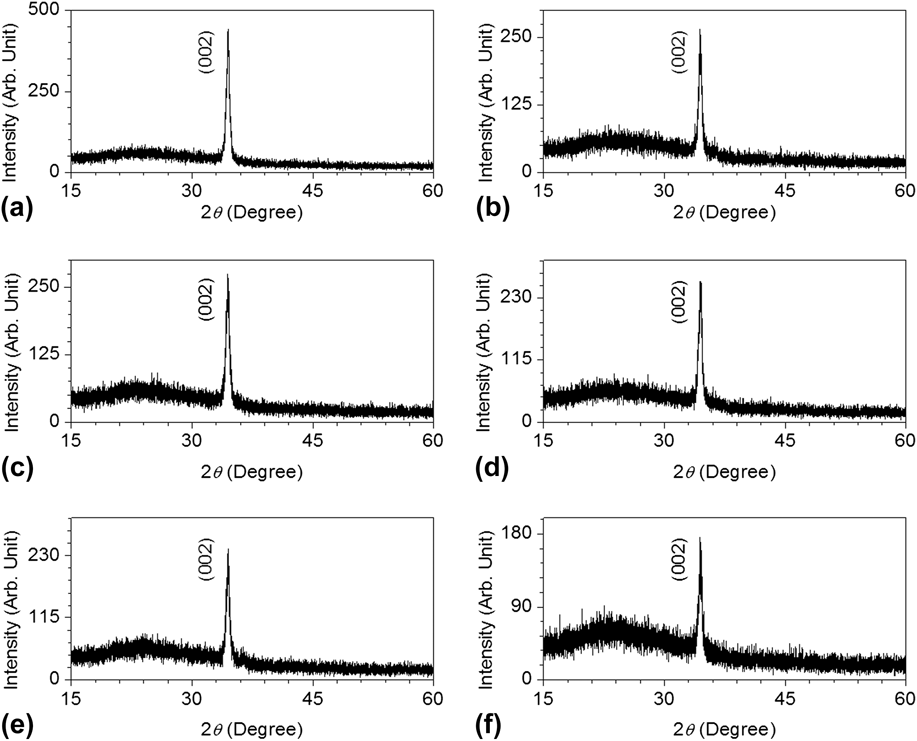
Figure 1 shows the XRD patterns of the annealed multilayered ZnO/Al/ZnO films with different mid-Al layer thicknesses. The results show that the multilayered films are crystalline. This is in good agreement with the published hexagonal wurtzite XRD patterns for ZnO films,Reference Hadis and Ümit4,Reference Song, Aberle and Xia13,Reference Sahu, Lin and Huang21,Reference Sahu and Huang33 without the midlayer Al phase. For comparison, the XRD pattern obtained from a single layered 50 nm thick ZnO film (after annealing at the same temperature and dwelling time) is presented in Fig. 2(a). These show the effect of midlayer Al thickness ranging from ∼1 to 10 nm. This is sandwiched between the upper and lower ZnO layers (each with a thickness of 25 nm). The results suggest that the mid-Al layer is too thin to be resolved by the XRD.
XRD patterns for the annealed multilayered ZnO/Al/ZnO films with fixed ZnO double layers thickness of 25 nm each and a midlayer Al thickness based on (a) 3 nm to (f) 8 nm.

However, as the midlayer Al thickness increases between ∼1 and 10 nm, the peak height of the preferred (002)-orientation decreases significantly, as shown in Fig. 1, for the multilayered films with mid-Al layer thicknesses between 3 and 8 nm. This change in the relative intensity of the (002) XRD peak by the introduction of thicker Al midlayers implies that the crystallinity of the multilayered ZnO/Al/ZnO films decreases as the mid-Al layer thickness is increased.
B. Optical properties
The optical properties of the multilayered ZnO/Al/ZnO films were measured as a function of the Al midlayer thickness. The solar transmittance spectra (in the visible region for the multilayered ZnO/Al/ZnO films with different Al midlayer thicknesses) are presented in Figs. 3(a)–3(d). For comparison, the solar transmittance profile obtained from a single layered 50 nm thick ZnO film (after annealing in air at 400 °C for 90 min) is also presented in Fig. 2(b). Increasing the Al midlayer thickness between ∼1 and 10 nm had only a slight effect on the transmission characteristics of the multilayered ZnO/Al/ZnO films.
(a) XRD pattern and (b) optical transmittance profile of a 50 nm thick ZnO thin film deposited on a glass substrate after annealing for 90 min at 400 °C in air.
The observed limitations in the optical transmittances of the multilayered film can be attributed to numerous factors. These include reflection losses that comprise both diffuse and specular scattering phenomena. These can arise mainly from interlayer surface roughness and interfacial defects, such as reacted and/or unreacted chemical species, including other oxide phases, trapped gases, and some impurities or inclusion atoms generated during the nonideal multilayered film processing.
Figure 4 presents the visible solar reflectance profiles obtained from the multilayered ZnO/Al/ZnO films. The result shows the other important causes of the decrease in multilayer transmittance. This depends on the thickness of mid-Al layer as a result of its reflective nature and the multiple interference phenomena which require that the average of the visible solar transmittances must be taken by the spectrophotometer used.Reference Bennett42 Furthermore, the transmittance in the multilayered films is decreased by multiple light absorptions, which are primarily due to the increasing free charge-carrier density from the mid-Al layers.
Solar transmittance curves in the visible region of the solar spectrum obtained from annealed multilayered ZnO (25 nm)/Al/ZnO (25 nm) films with different mid-Al layer thicknesses captioned in each plot.
Solar spectra reflectance profiles for the annealed multilayered ZnO (25 nm)/Al/ZnO (25 nm) films for the mid-Al layer thicknesses based on 0, 5, and 10 nm.
However, the average transmitted part of the incident photons in the multilayered films (with Al midlayer thickness ranges between 2 and 10 nm) is generally very good, that is between ∼85 and 90% in the visible region of the solar spectrum with wave lengths between ∼400 and 900 nm. These high transmittance values (in the visible region of the solar spectrum) are generally desirable for the optical performance of composite electrodes. They are attributed to the reductions in optical reflection (Fig. 4) and absorption by the ultra-thin Al midlayers that were sandwiched between the highly visible spectra transmitting ZnO film layers.
Furthermore, the observed high transmittances in multilayered films with relatively thick Al midlayers (between ∼6 and 10 nm) can be attributed to the crystal characteristics of the films shown in Fig. 1. Clearly, with increasing Al midlayer thickness, the light was less scattered because of the decreasing crystalline structure of the multilayered films. This resulted in higher solar transmittances in the visible region of the spectra. Figure 3 also shows that, with increasing Al midlayer thickness, the multilayered film absorption limits are shifted to shorter wave lengths. All of them lie within the ultraviolet (UV) region of the solar spectrum.
The absorption coefficients of the multilayered ZnO/Al/ZnO films were calculated using the well-known approximate spectrophotometry quadratic equation. This is given byReference Chopra and Bahl43,Reference Filippov and Shulitskii44
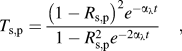 $${T_{{\rm{s,p}}}} = {{{{\left( {1 - {R_{{\rm{s,p}}}}} \right)}^2}{e^{ - {\alpha _\lambda }t}}} \over {1 - R_{{\rm{s,p}}}^2{e^{ - 2{\alpha _\lambda }t}}}}\quad {\rm{,}}$$
where t is the multilayered film thickness, which is obtained using surface profilometry measurement, so that the absorption coefficient αλ which is a function of wave length is determined from
 $${e^{ - {\alpha _\lambda }t}} = {{ - {{\left( {1 - R} \right)}^2} \pm {{\left[ {{{\left( {1 - R} \right)}^4} + 4{T^2}{R^2}} \right]}^{{1 \mathord{\left/ {\vphantom {1 2}} \right. \kern-\nulldelimiterspace} 2}}}} \over {2T{R^2}}}\quad {\rm{,}}$$
or equivalently from
 $${\alpha _\lambda } = - {1 \over t}\ln {1 \over {{R^2}}}\left[ {{{ - {{\left( {1 - R} \right)}^2}} \over {2T}} + {{\left( {{{{{\left( {1 - R} \right)}^4}} \over {4{T^2}}} + {R^2}} \right)}^{{1 \mathord{\left/ {\vphantom {1 2}} \right. \kern-\nulldelimiterspace} 2}}}} \right]\quad {\rm{.}}$$
Note that R and T are experimental reflectance and transmittance values, respectively. Subsequently, the apparent optical band gap energy, E 0, of the multilayered film is readily obtained usingReference Sivaramakrishnan and Alford3,Reference Al-Kuhaili, Al-Maghrabi, Durrani and Bakhtiari5
 $${\alpha _\lambda }\left( {h\nu } \right) = k{\left( {h\nu - {E_0}} \right)^{{1 \mathord{\left/ {\vphantom {1 2}} \right. \kern-\nulldelimiterspace} 2}}}\quad {\rm{,}}$$
where hν is the photon energy and k is a constant.
The dependence of the  ${\left( {{\alpha _\lambda }h\nu } \right)^2}$ on the thickness of Al midlayer (as a function of photon energy) is presented in Fig. 5. This was used to estimate the apparent band gap energies for the multilayered ZnO/Al/ZnO films. This was done generally by extrapolating the
 ${\left( {{\alpha _\lambda }h\nu } \right)^2}$ curves as a function of photon energy. The photon energy-intercepts at
 ${\left( {{\alpha _\lambda }h\nu } \right)^2} = 0$ give the apparent optical band gap energies of the films. With increasing midlayer Al thickness (from ∼0 to 10 nm), the result shows that the apparent band gap energy of the multilayered film increased from ∼3.26 to 3.85 eV, by ∼0.60 eV. Optically, this shift in band gap energy can be attributed to the increase in multilayered film free charge-carrier density with increasing mid-Al layer thickness. This leads to the Moss–Burstein effect,Reference Burstein41 in which filling of the states near the bottom of the conduction band by the charge carriers leads to shifting of the Fermi level position and widening of the optical band gaps of the multilayered films.
Plots of  ${\left( {{\alpha _\lambda }h\nu } \right)^2}$ as a function of photon energy, hν, showing the dependence of optical band gap energy of the ZnO (25 nm)/Al/ZnO (25 nm) films on the captioned mid-Al layer thicknesses.
The interpretation of the optical band gap energy results, based on the Moss–Burstein effect, assumes a sharp parabolic conduction band curvature, such that the shift in Fermi level position for free-electrons can be obtained. This is given byReference Chopra, Major and Pandya1
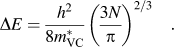 $$\Delta E = {{{h^2}} \over {8m_{{\rm{VC}}}^*}}{\left( {{{3N} \over \pi }} \right)^{{2 \mathord{\left/ {\vphantom {2 3}} \right. \kern-\nulldelimiterspace} 3}}}\quad {\rm{.}}$$
Subsequently, the widening of the optical band gap energy, E 0, is obtained fromReference Burstein41
 $${E_0} = {E_{\rm{G}}} + \Delta E\quad {\rm{,}}$$
where  $m_{{\rm{VC}}}^*$ is the combined conduction-valence band effective mass, N is the density of free electrons, and E G is the intrinsic minimum energy separation between the ZnO bands.
C. Electrical properties
Table I shows the average electrical sheet resistance (R s), resistivity (ρ), and the Haacke figures of merit,  ${\emptyset _{{\rm{TC}}}}$, obtained for the multilayered ZnO/Al/ZnO films. These were obtained as functions of Al midlayer thickness. The electrical properties of single layered ZnO films (without mid-Al layer) could not be measured due to their extremely high resistivity values. The latter was greater than the sensitivity limit of the four-point probe system that was used. As shown in Table I, when the thickness of Al midlayer was increased, both electrical sheet resistance and resistivity of the multilayered ZnO/Al/ZnO films were enhanced. There is an abrupt decrease in the electrical resistivity from 1.74 to 4.65 × 10⁻³ Ω cm, as the mid-Al layer thickness increased from ∼2 to 6 nm. Furthermore, the resistivity values decreased gradually to a minimum bulk value of between ∼ (8.07–3.62) × 10−4 Ω cm for the Al midlayer thicknesses in the range of ∼7–10 nm. The corresponding multilayered film sheet resistance dropped significantly from ∼1.73 × 10⁵ to 7.25 Ω/sq. for the mid-Al layer thickness of ∼2 and 10 nm, respectively.
List of Al intermediate layer thicknesses used for the RF deposition of the multilayered ZnO (25 nm)/Al/ZnO (25 nm) films and their corresponding multilayered film sheet resistances, electrical resistivities, and the Haacke figures of merit.
The transparent conductive properties for similar ZnO/Al/ZnO multilayer structures were reported initially by Al-Kuhaili et al.Reference Al-Kuhaili, Al-Maghrabi, Durrani and Bakhtiari5 They demonstrated the electro-optical properties of a multilayered ZnO/Al/ZnO film with fixed midlayer Al thickness of ∼20 nm and ZnO layer thickness of ∼200 nm. It was shown that the thickness, structural and electro-optical properties of the composite ZnO/Al/ZnO film depend significantly on the post-deposition annealing treatments. The best multilayered film electrode with average visible spectra transmittance of 75% and electrical sheet resistivity of 2.9 × 10⁻³ Ω cm was obtained at an optimal annealing temperature of 300 °C by these authors.Reference Al-Kuhaili, Al-Maghrabi, Durrani and Bakhtiari5
While Al-Kuhaili et al.Reference Al-Kuhaili, Al-Maghrabi, Durrani and Bakhtiari5 focused on a fixed midlayer of Al, in this work, the electrical and optical properties of the multilayered ZnO/Al/ZnO film structures presented include the effects of different midlayer Al thicknesses ranging between ∼1 and 10 nm. In comparison, the electro-optical properties obtained by Al-Kuhaili et al.Reference Al-Kuhaili, Al-Maghrabi, Durrani and Bakhtiari5 are largely in agreement with the current results. However, the differences between our results and those of Al-Kuhaili et al.Reference Al-Kuhaili, Al-Maghrabi, Durrani and Bakhtiari5 are due to differences in the fabrication technique (thermal evaporation versus RF magnetron sputtering) that was used. Furthermore, the initial raw materials (ZnO and Al pellets), deposition rates, and annealing temperatures were different as well as the thicker ZnO and mid-Al layers used in the study by Al-Kuhaili et al.Reference Al-Kuhaili, Al-Maghrabi, Durrani and Bakhtiari5
Also, the electrical results obtained for the multilayered ZnO/Al/ZnO films are comparable with the earlier published results for other multilayered ZnO/metal/ZnO film systems with goldReference Sivaramakrishnan and Alford3 or copperReference Sahu and Huang35 metallic intermediate layers. The observed trends are attributed to the increase in free charge-carrier densityReference Al-Kuhaili, Al-Maghrabi, Durrani and Bakhtiari5 and mobility in the multilayered films. These increase with increasing midlayer metallic thickness. However, during deposition by RF magnetron sputtering, the ultra-thin metallic layers are known to form discontinuous films on top of the oxides.Reference Sivaramakrishnan and Alford3,Reference Dhar and Alford26,Reference Choi, Kim, Lee and Kim27,Reference Sahu and Huang34 These result in high combined multilayered film resistivities, which decrease significantly with increasing film thickness in the metallic layers.Reference Sivaramakrishnan and Alford3 Thus, as the mid-Al thickness increases, the layer gradually changes from discontinuous to continuous, after reaching a critical transition thickness (t c). At the discontinuous–continuous transition thickness, the multilayered films are also known to adopt different charge-carrier transport mechanisms.Reference Sivaramakrishnan and Alford3 This leads to the observed gradual decrease in electrical properties with increasing mid-Al layer thickness between 7 and 10 nm.
Further evidence of the onset of the mid-Al layer discontinuous–continuous transition phenomena is presented in Table I and Figs. 1 and 5. The filling of the states near the bottom of the conduction band (as a result of the increasing Al midlayer thickness) is associated with an increase in free charge-carrier density and mobility. This is further attributed to the widening of the optical band gap (Fig. 5). This results in an increase in the electrical conductivity in the multilayered film structure (Table I). The sharp increase in apparent optical band gap energy was observed for midlayer Al thicknesses between ∼8 and 10 nm. This suggests the onset of ZnO–Al charge-carrier density and conductivity transitions, resulting mainly from the merging of the lower and upper ZnO layers with the continuous mid-Al layer.
Furthermore, as shown in Fig. 1, as the Al midlayer thickness increases, the crystallinity of the multilayered film structure decreases. This implies that, in the multilayered ZnO/Al/ZnO films with thick Al intermediate layers (that were relatively thicker than the t c), some charge carriers are bound in the short range by the nonuniform amorphous structure. This is partly the reason for the bulk resistivity values which are generally steady with increasing Al thickness, for multilayered films with thicker Al midlayers between ∼7 and 10 nm (Table I).
A Haacke figure of merit,  ${\emptyset _{{\rm{TC}}}}$ (shown in Table I), was estimated for each of the multilayered ZnO/Al/ZnO film system. This was done using the well-known Haacke figure of merit equation. This is given byReference Chopra, Major and Pandya1,Reference Sivaramakrishnan and Alford3,Reference Dhar and Alford26
 $${\phi _{{\rm{TC}}}} = {{T_{{\rm{av}}}^{10}} \over {{R_{\rm{s}}}}}\quad {\rm{,}}$$
where T av is the average transmittance of a given multilayered film. Note that the larger the value of  ${\emptyset _{{\rm{TC}}}}$, the better the performance of a transparent conductor. As shown in Table I, at the mid-Al layer thickness range of ∼7–10 nm, the multilayered film attained higher Haacke figures of merit between ∼1.25 × 10⁻³ and 4.72 × 10⁻³ Ω−1. These values compare well with the published values for multilayer films with Au intermediate layers, in which
 ${\emptyset _{{\rm{TC}}}}$ between ∼8.3 × 10⁻³ and 15.1 × 10⁻³ Ω−1 at the mid-Au layer thickness between 6 and 12 nm has been reported.Reference Sivaramakrishnan and Alford3 This suggests that the multilayered ZnO/Al/ZnO thin films can be synthesized as host material alternatives to ITO or ITO/metal/ITO TEs for applications in large area solar cells, light emitting diodes, and the other layered electronics and optoelectronic devices.
D. Implications
The practical implications of the current work are quite significant. First, the Haacke figures of merit obtained for the multilayered electrodes are comparable to those reported earlier for ITO-based electrodes that have  ${\emptyset _{{\rm{TC}}}}$ values between ∼2.07 × 10⁻³ and 3.82 × 10⁻² Ω−1.Reference Khusayfan and El-Nahass45 This suggests that the multilayered ZnO/Al/ZnO films have the potential to replace ITO in future TEs and anodes in solar cells and light emitting devices. The attractive combinations of optical and electrical properties are also promising for potential applications of ZnO/Al/ZnO composite TEs in solar cells and light emitting devices.
However, further work is required to test the performance of the composite electrodes in actual solar cells and light emitting devices. Such work should explore the current–voltage characteristics (fill factors, power conversion, and external quantum efficiencies), degradation mechanisms, and the long term performance characteristics of solar cells and light emitting devices fabricated with ZnO/Al/ZnO composite electrodes on glass substrates. These are clearly some of the challenges and opportunities for future work. Such work is particularly important due to the limited availability of indium (used in ITO films) for the wide range of applications in electronic structures and components.
IV. SUMMARY AND CONCLUDING REMARKS
This study presents the combined experimental and theoretical results of the transparent conductive properties of layered composite ZnO/Al/ZnO thin films. High transparent conductive properties were achieved in the annealed multilayered film sandwiches deposited on glass substrates by RF magnetron sputtering method. The multilayered films were characterized by examining the effects of Al midlayer thicknesses between ∼1 and 10 nm on the structural, optical, and electrical properties. The multilayered ZnO/Al/ZnO films annealed at 400 °C for 90 min exhibited high crystalline structures which decreased with increasing Al midlayer thickness. The electrical resistivity and sheet resistance of the multilayered films decreased with increasing mid-Al layer thickness. The corresponding apparent optical band gap energy increased with increasing mid-Al layer thickness.
The multilayered films with midlayer Al thicknesses in the range of ∼7–10 nm had low resistivity values between 3.62 × 10⁻⁴ and 8.07 × 10⁻⁴ Ω cm. They also had optical band gap energies of between ∼3.6 and 3.84 eV. The average solar transmittances of the multilayered films were above 85% in the visible region of the solar spectrum. For the midlayer Al thickness of 8 nm, the multilayered film exhibited the best Haacke figure of merit of 4.72 × 10⁻³ Ω−1 and an electrical resistivity of 4.91 × 10⁻⁴ Ω cm. This compares favorably to the one of commercially available ITO, for which films with resistivities of ∼1 × 10⁻⁴ Ω cm have been reported.Reference Luka, Krajewski, Witkowski, Wisz, Virt, Guziewicz and Godlewski39 This suggests that low resistivity multilayered ZnO/Al/ZnO film electrodes can be synthesized and that the electrodes are potentially good candidates as material alternatives to ITO or ITO/metal/ITO for applications in large area solar cells and other active or passive electronics and optoelectronic devices.
ACKNOWLEDGMENTS
The research was supported by grants from the World Bank STEP-B Program, the World Bank African Centers of Excellence Program, the African Development Bank, the African Capacity Building Foundation, and the Nelson Mandela Institution. Appreciation is also extended to Mrs. K. Onogu of Physics Advanced Laboratory, SHESTCO, Nigeria, for technical assistance with laboratory techniques.