Introduction
Hydrogen is arguably one of the most attractive fuels due to its high energy content per unit mass (120 J/g, about three times that of gasoline) and clean by-product, water, when consumed for energy generation.Reference Ogden1–Reference Li and Zhang6 However, its generation, storage, and usage on a large scale and at a low cost have been met with significant challenges. Currently, the dominant technology for direct hydrogen production is steam reforming that involves reactions between steam and hydrocarbons mostly based on fossil fuel.Reference Singh, Sharma, Sarma and Phanjoubam7 Storage of hydrogen with high mass or volume density and at ambient temperature and pressure has been extremely difficult.Reference Schuth8 Fuel cells are still high in cost in comparison to competitive technologies, such as gasoline internal combustion engines.Reference Kong, Hua, Pu, Chi and Jian9
Even given all of these challenges, the attraction of hydrogen as a clean fuel has continued to stimulate interest in research and development in generation, storage, and usage. On the generation front, one key focus has been on developing low-cost materials and strategies. One of the most attractive approaches for hydrogen generation is solar water splitting that uses solar light as the source of energy and water as the source of hydrogen, via processes such as photocatalysis or photoelectrochemistry. Photoelectrochemical (PEC) water splitting is attractive due to its potential high efficiency, up to >30% in principle, low cost, and environmental friendliness.Reference Bak, Nowotny, Rekas and Sorrell2
Nanostructured materials offer unique advantages for potential PEC applications.Reference Li and Zhang6 First, nanoscale sizes are comparable to carrier scattering lengths, significantly reducing the scattering rate and increasing carrier collection efficiency. Second, nanomaterials have strong absorption coefficients due to an increase of oscillator strength, thereby enabling high conversion efficiency. Third, the bandgap of nanomaterials (e.g., quantum dots [QDs]) can be tuned to absorb in a particular wavelength by varying size and, in principle, cover the whole solar spectrum. Fourth, the electronic band structure can be controlled by doping. Finally, bottom-up growth approaches, which use smaller components to produce larger and more complex structures, allow scalable synthesis of single crystal nanostructures on flexible substrates under mild conditions, leading to light weight and low cost.
In this review, we will focus on some recent progress on the study of metal oxide (MO) nanomaterials for PEC hydrogen generation, with emphasis on new strategies developed to enhance PEC efficiency. Efforts have been made to control morphological features, such as nanostructure size, shape, and surface characteristics, to improve PEC performance. While most research efforts have been on the experimental front, relevant theoretical and computation studies are important and starting to emerge, which should help to collaborate and guide further experimental investigations.
Principle of photoelectrochemical hydrogen generation
While the principle of PEC hydrogen generation is relatively simple, the underlying fundamental processes are complex and still not well understood at the molecular level. A typical PEC device consists of a photoanode and cathode immersed in water containing some electrolyte. The photoanode is typically a semiconductor that absorbs light and generates excitonsReference Frenkel10, Reference Wannier11 or electron–hole-pairs.Reference Zhang12 The electrons are transported to a metal cathode (e.g., Pt), often aided by an external bias that can come from a solar cell or from the electrical grid. Hydrogen generation occurs at the cathode from the reduction of protons by the electrons. On the photoanode, the holes left behind oxidize water molecules into oxygen gas and protons. The protons generated at the photoanode then diffuse and travel to the cathode. There are many more complicated variations of PEC devices,Reference Bak, Nowotny, Rekas and Sorrell2, Reference Miller and Vayssieres13 but the basic underlying principle is the same or very similar.
During steady-state operations of a PEC device, the photo-induced current is directly related to the performance of hydrogen generation, and the efficiency of photon-to-hydrogen generation (η) is the ratio of power used in water splitting to the input light power.Reference Miller and Vayssieres13 Assuming all the electrons-holes are consumed in the redox reaction, η can be calculated using the equationReference Bak, Nowotny, Rekas and Sorrell2

where I is the photocurrent (in amps), 1.23 V is the theoretical potential required for water splitting, V bias (in volts) is the applied external potential, J light (W/m2) is the light irradiance, and A is the irradiated area (m2). The efficiency of a PEC device also may be evaluated by incident photon-to-current conversion efficiency (IPCE), which is the amount of photogenerated electrons collected at the back contact per photon irradiated on the PEC surface:

I PH is the generated photocurrent density (A/m2), λ is the incident light wavelength (nm), P light is the photon flux (W/m2), and 1240 is the unit correction factor. IPCE reveals the photoresponse of the semiconductor photoanode as a function of the incident wavelength.
There are four fundamental steps involved in PEC that determine the overall performance for hydrogen generation:Reference Miller and Vayssieres13 (1) light absorption and charge carrier generation in the solid; (2) charge separation and transport in the solid and at the solid-liquid interface; (3) charge carrier extraction and electrochemical product formation at the solid-liquid interface; and (4) management of the electrochemical products in solution.
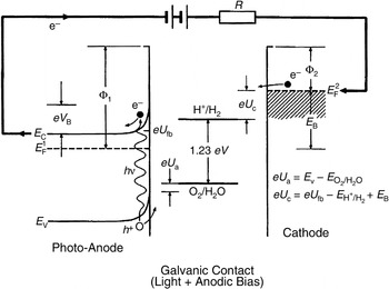
Figure 1 illustrates the energy levels involved in a typical n-type semiconductor photoanode. Band bending at the solid-liquid interface is critical for the initial photo-induced charge separation or exciton dissociation. Subsequent charge transport depends strongly on the morphological and structural details of the photoanode.Reference Bak, Nowotny, Rekas and Sorrell2, Reference Miller and Vayssieres13 Associated with each step, there are undesired loss mechanisms such as recombination, trapping, slow reaction due to overpotential, and disrupted mass transport.Reference Miller and Vayssieres13 Thus, a major focus in PEC research is on improving materials properties of the photoanode and minimizing unwanted processes.
Energy diagram of photoelectrochemical components: photoanode (n-type semiconductor), cathode (metal), and liquid electrolyte, with galvanic contact, light illumination, and applied external bias. E F, Fermi level;  , Fermi level for photoanode;
 , Fermi level for cathode; R, resistance; e–, electrons; h+, hole; Φ1 and Φ2, work functions for the photoanode and cathode, respectively; U a, overpotentials for the anode; U c, overpotential for cathode; E CB, energy of the bottom of the conduction band; E VB, energy for the top of the valence band; h, Planck’s constant; ν, frequency; e, electron charge; U fb, flat band potential; E B, potential energy related to the bias; V B, surface potential (corresponding to band curvature);
 , energy of the redox couple H+/H2;
 , energy of the redox couple O2/H2O. Reproduced with permission from Reference Reference Bak, Nowotny, Rekas and Sorrell2. ©2002, Elsevier.

Single component metal oxide systems for photoelectrochemical H2 generation
For ease of discussion, we will divide the discussion based on the material used for the PEC photoelectrode. In this section, we will focus on photoelectrodes that are primarily based on single-component metal oxides that do not require other materials as sensitizers or dopants. As most MOs do not have visible absorption, their usage for solar hydrogen generation is limited. However, there have been many fundamental studies of PEC cells based on single-component MOs. For example, nanostructured MO semiconductor materials that have been studied for PEC cells include WO3,Reference Bedja, Hotchandani, Carpentier, Vinodgopal and Kamat14–Reference Wolcott, Kuykendall, Chen, Chen and Zhang18 ZnO,Reference Ahn, Shet, Deutsch, Jiang, Yan, Al-Jassim and Turner19–Reference Yan, Ahn, Shet, Deutsch, Huda, Wei, Turner and Al-Jassim21 Fe2O3,Reference Lindgren, Wang, Beermann, Vayssieres, Hagfeldt and Lindquist22–Reference Saretni-Yarahmadi, Wijayantha, Tahir and Vaidhyanathan24 and, more commonly, TiO2.Reference Mishra, Shukla and Srivastava25–Reference Khan and Sultana37
Compared to 0D nanostructures (e.g., spherical NPs), 1D nanostructures, such as nanorods and nanowires, are expected to exhibit improved transport properties. In comparison to NPs, nanorods should improve the transport of charge carriers and thus reduce the recombination losses at grain boundaries due to vectorial, or directional, charge transport along the long axis. Moreover, the small diameter of nanorods can minimize the distance for holes to diffuse to the semiconductor/electrolyte interface. The first demonstration of PEC water splitting using 1D nanostructures used hematite nanorod arrays as the photoelectrode.Reference Lindgren, Wang, Beermann, Vayssieres, Hagfeldt and Lindquist22, Reference Beermann, Vayssieres, Lindquist and Hagfeldt38 The unique advantages offered by nanorod arrays also have been observed in other semiconductors such as TiO2Reference Wolcott, Smith, Kuykendall, Zhao and Zhang31, Reference Khan and Sultana37 and ZnOReference Ahn, Shet, Deutsch, Jiang, Yan, Al-Jassim and Turner19 and subsequently further extended to their various nanotube structures.Reference Lin, Lu, Hsieh and Chien28, Reference Eder, Motta and Windle30, Reference Mor, Varghese, Wilke, Sharma, Shankar, Latempa, Choi and Grimes32, Reference Park, Kim and Bard35, Reference Mor, Shankar, Paulose, Varghese and Grimes39–Reference Varghese and Grimes46 In comparison to nanorods or nanowires, nanotubes have less material for light absorption but higher surface area for redox reactions.
TiO2
The most extensively studied MO system is TiO2, which commonly exists in anatase (bulk bandgap 3.18 eV) and rutile (bulk bandgap 3.03 eV) phases. Like many MOs, TiO2 is abundant and stable and has appropriate energy levels for photovoltaic (PV) and PEC applications. The major limitation is weak absorption in the visible spectrum. Most studies of PEC based on TiO2 nanostructures utilize NPs.Reference Mishra, Shukla and Srivastava25–Reference Eder, Motta and Windle30, Reference Mor, Varghese, Wilke, Sharma, Shankar, Latempa, Choi and Grimes32–Reference Park, Kim and Bard35, Reference Cowan, Tang, Leng, Durrant and Klug47 In general, UV illumination is needed, and the PEC efficiency is low, less than 1%, especially in the visible range.
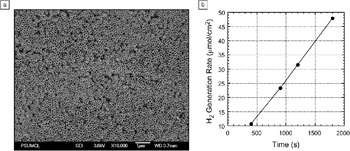
Recent efforts have focused more on 1D nanostructures that are expected to have better charge transport properties.Reference Wolcott, Smith, Kuykendall, Zhao and Zhang31, Reference Khan and Sultana37, Reference Hensel, Wang, Li and Zhang48 When the photoresponse of n-TiO2 thin films and nanowire electrodes for water splitting was compared, a more than twofold increase in maximum photoconversion efficiency was observed for the nanowires.Reference Khan and Sultana37 Similarly, the photosplitting of water using highly ordered TiO2 nanotube arrays, shown in Figure 2a, has been reported.Reference Mor, Shankar, Paulose, Varghese and Grimes39 The nanotube wall thickness was found to be a key parameter influencing the magnitude of the photoanodic response and the overall efficiency of the water splitting. Upon 320–400 nm illumination, hydrogen gas was generated at an overall conversion efficiency of 6.8% (Figure 2b), which was the highest reported value in TiO2-based PEC cells to date.
Titania nanotube arrays used as a photoanode for hydrogen generation in a photoelectrochemical cell. (a) Scanning electron microscopy images of titania nanotube arrays prepared via anodization. (b) Hydrogen photoproduction in a photoelectrochemical cell consisting of a titania nanotube array photoanode and Pt mesh cathode. Reproduced with permission from Reference Reference Mor, Shankar, Paulose, Varghese and Grimes39. ©2005, American Chemical Society.

It is clear that the PEC performance is related to the electronic and structural properties of nanorod arrays. Major efforts have been placed on developing a new synthetic strategy for improving the density, morphology, and material quality of MO nanorod arrays tailored for PEC applications.Reference Li and Zhang6, Reference Wolcott, Smith, Kuykendall, Zhao and Zhang31 Given the many studies of PEC cells based on TiO2 nanostructures, quantitative and rigorous comparisons between 0D and 1D structures are still lacking, partly because such comparisons can be tricky due to their dependence on characteristics such as morphology, surface, impurities, and details of films or device architectures. Further work is needed in this direction. More complex nanostructures such as nanospiders of TiO2 have been reported for PEC H2 generation recently.Reference Fei, Yang, Rogow, Fan and Oliver49
ZnO
Similar to TiO2, ZnO is another MO system that has received considerable attention for various purposes, including PEC. ZnO is extremely rich in nanostructures, ranging from nanowires to nanobelts and nanoflowers.Reference Liu, Kim, Wang, Palmer, Chen, Bruinsma, Bunker, Exarhos, Graff, Rieke, Fryxell, Virden, Tarasevich and Chick50–Reference Yang, Wolcottt, Wang, Sobo, Fitzmorris, Qian, Zhang and Li54 Its common and stable crystal structure is hexagonal wurtzite with a bulk bandgap of 3.3 eV, similar to that of TiO2. However, it has some subtle differences compared to TiO2 regarding photoelectrical properties, where ZnO is usually less efficient. This lower efficiency is possibly due to their differences in the electron occupancy of the d-orbitals.Reference Anderson and Lian55 For PEC applications, most studies have focused on ZnO films or NPs.Reference Wolcott, Smith, Kuykendall, Zhao and Zhang52, Reference Gupta, Sharma, Shrivastava, Solanki, Singh, Satsangi, Dass and Shrivastav56, Reference Shet, Ahn, Deutsch, Wang, Nuggehalli, Yan, Turner and Al-Jassim57 Recent efforts have shifted toward 1D or more complex nanostructures.Reference Ahn, Shet, Deutsch, Jiang, Yan, Al-Jassim and Turner19, Reference Yang, Wolcottt, Wang, Sobo, Fitzmorris, Qian, Zhang and Li54, Reference Ahn, Yan, Shet, Jones, Deutsch, Turner and Al-Jassim58, Reference Wang, Zhu, Xu, Wang, Tao, Hark, Xiao and Li59
WO3
Nanostructured WO3 has been studied for PEC applications in various structural forms, including thin films and NPs,Reference Wang, Lindgren, He, Hagfeldt and Lindquist15, Reference Hotchandani, Bedja, Fessenden and Kamat60–Reference Hong, Jun, Borse and Lee63 nanowires,Reference Chakrapani, Thangala and Sunkara64 and nanodisks.Reference Wolcott, Kuykendall, Chen, Chen and Zhang18 Compared to single-crystalline WO3, the absorption edge of amorphous or nanostructured WO3 shows a substantial shift to lower energy.Reference Alexander, Augustynski and Vayssieres65 Nanocrystalline WO3 usually has reasonably strong absorption and thereby produces a photocurrent in the 400–450 nm region. Due to weak visible absorption (>450 nm), various strategies, such as doping and dye to QD sensitization, are needed to enhance its visible absorption and PEC properties, as discussed further in the binary metal oxide nanostructures section.
Fe2O3
α-Fe2O3 is representative of a few MO systems that have strong visible absorption.Reference Cornell and Schwertmann66 The visible absorption makes Fe2O3 highly attractive for PEC and other applications. Unfortunately, Fe2O3 often shows weak PEC performance,Reference Tahir, Wijayantha, Saremi-Yarahmadi, Mazhar and McKee67, Reference Boumaza, Boudjemaa, Omeiri, Bouarab, Bouguelia and Trari68 mainly due to very short-lived charge carrier lifetimes that are likely caused by a high density of defect or trap states.Reference Cherepy, Liston, Lovejoy, Deng and Zhang69, Reference Satsangi, Dass, Shrivastav and Vayssieres70 Recent studies using vertically aligned and highly ordered nanorods and nanotubes have demonstrated strong photocurrent,Reference LaTempa, Feng, Paulose and Grimes71, Reference Mao, Han and Park72 attributed to improved light harvesting and charge transport in these 1D nanostructures. PEC cells prepared from these nanorod arrays showed about 8 mA/cm2 photocurrent density under 1 sun condition, which is claimed to be the highest value obtained from α-Fe2O3.
Binary metal oxide nanostructures
Binary MO nanostructures refer to systems with two different MOs or with one MO coupled with another material, such as a dopant or sensitizer. These structures are designed to alter and improve their optical and electronic properties for PEC or other applications.
Mixed metal oxides
Two MO semiconductors can be used together to manipulate the electronic band structure and improve their optical and electronic properties (e.g., increasing visible absorption and reducing electron–hole recombination) for PEC or PV applications. Examples include SnO2/TiO2,Reference Nasr, Kamat and Hotchandani73 TiO2/WO3,Reference Saeki, Okushi, Konno and Furuichi74 and SnO2/ZnO.Reference Kumara, Tennakone, Kottegoda, Bandaranayake, Konno, Okuya, Kaneko and Murakami75 Recently, Fe2O3 has been used to modify TiO2 nanotube arrays for enhancing visible absorption for PEC.Reference Kuang, Yang, Luo and Cai76 Generally, multicomponent nanostructures, when properly combined, help to improve the performance of the PEC over that based on individual components by increasing light absorption and counteracting the electron–hole recombination process.Reference Kumara, Tennakone, Kottegoda, Bandaranayake, Konno, Okuya, Kaneko and Murakami75
Dye sensitization
Similar to dye-sensitized solar cells, in which the charge injection from dye molecules into metal oxides is used for electricity generation, dye sensitization has been used to improve PEC reactions by increasing visible light absorption and overall photoconversion.Reference Cahen, Hodes, Gratzel, Guillemoles and Riess77–Reference Caramori, Cristino, Argazzi, Meda and Bignozzi80 One of the earlier studies suggests that long-lived charge separation in a nanostructured TiO2 membrane sensitized with Ru complexes is possible for water splitting.Reference Hoyle, Sotomayor, Will and Fitzmaurice81 Recently, nanoparticulate anatase TiO2 sensitized with ruthenium polypyridyl dyes showed enhanced visible light–induced water splitting.Reference Youngblood, Lee, Kobayashi, Hernandez-Pagan, Hoertz, Moore, Moore, Gust and Mallouk82
Another recent study using TiO2 photoanodes sensitized with ruthenium(II) polypyridine complexes for PEC H2 generation has shown that the photoanodes sustained 240 h of irradiation without undergoing appreciable hydrolysis and decomposition in an aqueous environment at pH 3, which is much longer than previously reported.Reference Caramori, Cristino, Argazzi, Meda and Bignozzi80 The use of organic sacrificial donors considerably enhanced the photoanodic response, and the photoelectrode in contact with an organic solvent showed high photocurrent, with an electrolysis yield close to 87%.
Quantum dot sensitization
Similar to the idea behind two mixed MOs for band structure manipulation, QDs can be used in conjunction with a MO to alter the electronic structure. QDs with smaller bandgaps than the MO also can be considered as sensitizers, similar to dye molecules but with the advantages of potentially higher stability and size-tunable absorption. Examples include TiO2/CdS,Reference Lin, Lu, Hsieh and Chien28, Reference Chen, Paulose, Ruan, Mor, Varghese, Kouzoudis and Grimes40, Reference Yin, Jin and Hou45, Reference Park, Choi and Hoffmann83–Reference Chi, Lee and Weng85 TiO2/CdSe,Reference Liu and Kamat86 and ZnO/CdS.Reference Hotchandani and Kamat87 Efficient electron injection requires that the bottom of the conduction band of the QDs be above the bottom of the CB of the MO.Reference Kamat88 The electron transfer between the QDs and MO could also enhance the charge separation and inhibit recombination by forming a potential gradient at the interface.
Similarly, QDs have been utilized to sensitize 1D MO nanostructures for water splitting.Reference Lin, Lu, Hsieh and Chien28, Reference Chen, Paulose, Ruan, Mor, Varghese, Kouzoudis and Grimes40, Reference Tak, Hong, Lee and Yong89 CdS QDs deposited on ZnO nanowires increased the light absorption onset up to ~550 nm, and a PEC study showed enhanced photocurrents compared to those of a bare ZnO nanowire photoanode.Reference Tak, Hong, Lee and Yong89 Likewise, TiO2 nanorod arrays have been sensitized by different sized CdSe NPs to form rainbow solar structures that showed improved PV performance because of their ability to absorb in a broad range of wavelengths in the visible region.Reference Kongkanand, Tvrdy, Takechi, Kuno and Kamat90 In a recent study, vertically aligned ZnO/CdTe core-shell nanocable arrays have been fabricated and demonstrated to exhibit excellent photovoltaic properties.Reference Wang, Zhu, Xu, Wang, Tao, Hark, Xiao and Li59 Such 1D nanostructures should be easily extended to PEC applications, as has been demonstrated recently in CdSe QD-sensitized TiO2 nanorods.Reference Hensel, Wang, Li and Zhang48
In other related studies, increasing structural complexity of heterogeneous nanostructures has been found to further improve the efficiency and stability of PEC cells. For example, various core/shell nanowire heterostructures (e.g., CdS/TiO2 and Si/TiO2) have been studied for PEC water splitting.Reference Hwang, Boukai and Yang29, Reference Yin, Jin and Hou45 Properly designed QD/MO binary systems can help to address the shortcomings of individual semiconductors such as photoanode to improve PEC performance.
Doping
Doping is well known to be an effective way to alter the optical and electronic properties of semiconductors or MOs for different applications. A large number of dopants for MOs have been studied, including metal ions such as iron and copperReference Eder, Motta and Windle30, Reference Anpo, Matsuoka, Mishima and Yamashita91–Reference Ingler and Khan93 or nonmetal species such as nitrogenReference Yan, Ahn, Shet, Deutsch, Huda, Wei, Turner and Al-Jassim21, Reference Cui, Ma, Zhang, Yang and Zhang33, Reference Randeniya, Bendavid, Martin and Preston94, Reference Reyes-Gil, Reyes-Garcia and Raftery95 and carbon.Reference Xu, Shaban, Ingler and Khan44, Reference Sakthivel and Kisch96 When doped with metal ions such as Ru3+ and Cr3+, MOs such as TiO2 showed much higher efficiency PEC activities, attributed to decreased effective bandgap or intra-bandgap states that result in visible light absorption.Reference Kato and Kudo97 However, in many cases, the metal ions act as traps of photogenerated carriers and do not effectively narrow the bandgap.Reference Choi, Termin and Hoffmann98, Reference Khan, Al-Shahry and 99
Anionic non-metal doping has attracted strong interest in recent years.Reference Asahi, Morikawa, Ohwaki, Aoki and Taga100 For instance, TiO2 has been doped with elements such as C, S, and N.Reference Park, Kim and Bard35, Reference Gole, Stout, Burda, Lou and Chen101–Reference Murakami, Kasahara and Nosaka103 N-doping, in particular, has been found to be very effective in extending the visible absorption of TiO2.Reference Gole, Stout, Burda, Lou and Chen101, Reference Burda, Lou, Chen, Samia, Stout and Gole104–Reference Chen, Nambu, Wen, Graciani, Zhong, Hanson, Fujita and Rodriguez111 Similarly, an enhanced photoresponse of C-doped TiO2 has been reported.Reference Khan, Al-Shahry and 99 In addition, C doping of vertically aligned TiO2 nanotube arrays showed much more efficient water splitting.Reference Park, Kim and Bard35
Non-metal doping also has been demonstrated in other MOs such as ZnO and Fe2O3. N-doped ZnO film has shown a significant red-shift in light absorption.Reference Ahn, Shet, Deutsch, Jiang, Yan, Al-Jassim and Turner19–Reference Yan, Ahn, Shet, Deutsch, Huda, Wei, Turner and Al-Jassim21 Vertically aligned single-crystal ZnO nanowire arrays were synthesized by a hydrothermal method and doped with N.Reference Yang, Wolcottt, Wang, Sobo, Fitzmorris, Qian, Zhang and Li54 A PEC study demonstrated significant enhancement of the photoresponse and an order of magnitude increase in photocurrent density compared to pristine ZnO nanowires.
Recent studies showed a strong synergistic effect between N-doping and QD-sensitization of TiO2 for both PVReference Lopez-Luke, Wolcott, Xu, Chen, Wcn, Li, De La Rosa and Zhang112 and PEC applications.Reference Hensel, Wang, Li and Zhang48 The effect is tentatively attributed to enhanced hole transfer/transport due to an increase in oxygen vacancy energy levels near the top of the valence band of the CdSe QDs due to N-doping.Reference Hensel, Wang, Li and Zhang48
Tandem cells
Similar to multijunction tandem solar cells, tandem PEC cells have been designed and evaluated as a way to improve device performance. The idea is to have more than one PEC cell stacked up in various configurations to enhance light absorption and increase overall cell voltage or photopotential, which typically comes with a reduction in photocurrent that is undesired for hydrogen generation.Reference Miller and Vayssieres13 For instance, in a self-driven p/n-Fe2O3 tandem PEC cell, a photoanode and photocathode, both deposited onto transparent substrates, are stacked one in front of the other and electrically connected by a wire.Reference Ingler and Khan113
In another study, highly ordered TiO2 nanotubular arrays grown on both sides of a Ti foil have been used as both photoanode (carbon-doped titania nanotubes) and cathode (Pt NPs dispersed on TiO2 nanotubes; PtTiO2/Ti/PtTiO2) in a specially designed PEC cell to generate hydrogen by water.Reference Mohapatra, Mahajan and Misra42 The approach was suggested to be suitable for large-scale hydrogen generation using renewable energy sources.
A similar approach has been explored for PEC/PV hybrid electrodes.Reference Morisaki, Watanabe, Iwase and Yazawa114, Reference Miller, Rocheleau and Deng115 The idea of combining PEC with PV cells was first demonstrated for bulk TiO2 photoanode and Si solar cell, with very low overall efficiency (0.1%) achieved since many parameters involved were not optimized.Reference Morisaki, Watanabe, Iwase and Yazawa114 More recently, it was demonstrated that a PEC top junction can be monolithically stacked with a solid-state PV bottom junction that was connected to a counter-electrode.Reference Miller, Rocheleau and Deng115 Careful design considerations must be given in such tandem device structure, not the least of which are the energy levels of the materials involved for the PEC and PV.
Ternary components or more complex metal oxide nanostructures
In order to improve the PEC properties of MOs, more complex structures or architectures have been developed (e.g., structures with more than two components of different materials). Such structures afford the flexibility to alter the electronic band structure for possibly improving their optical and electronic properties. However, their complexity usually increases, and rational design and a good fundamental understanding of their properties become more essential.
Combined sensitization and doping: Synergistic effect
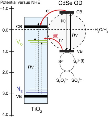
Very recently, a strong synergistic effect has been found when TiO2 is simultaneously doped with nitrogen (TiO2:N) and sensitized with CdSe QDs for both solar cellsReference Lopez-Luke, Wolcott, Xu, Chen, Wcn, Li, De La Rosa and Zhang112 and PEC hydrogen generation.Reference Hensel, Wang, Li and Zhang48 The photocurrent was found to be greatly enhanced when CdSe QDs sensitized TiO2:N as compared to undoped TiO2, even though the difference in the photocurrent for unsensitized TiO2 and TiO2:N was very small due to the low doping level. Therefore, there is clearly a synergistic effect between nitrogen doping and QD sensitization. It was suggested that hole transfer is enhanced by increased oxygen vacancy levels due to N-doping, which facilitates overall charge transfer/transport and reduces electron and hole recombination and enhances photocurrent (Figure 3).Reference Hensel, Wang, Li and Zhang48
Proposed model for the electron transfer at CdSe/TiO2 interface in a CdSe-TiO2:N sample. All the energy levels are referenced to normal hydrogen electrode (NHE) scale. CB and VB are the conduction band and valence band edges, respectively. Green lines and blue lines represent the energy levels of VO and NE respectively. Three possible competing pathways for the photogenerated holes in CdSe are shown: (i) oxidization of S2– to  ; (ii) recombination with electrons in the conduction band, and (iii) transfer to VO levels in TiO2. QD, quantum dot; h, Planck’s constant; ν, frequency; NE, nitrogen atom energy levels; VO, vacancy on an oxygen site. Reproduced with permission from Reference Reference Hensel, Wang, Li and Zhang48. ©2010, American Chemical Society.

Co-sensitization
Sensitization of MO nanostructures with more than one sensitizer has been explored as a potential means to enhance PEC performance. For example, CdSe and CdS QD co-sensitization of TiO2 photoelectrodes has been demonstrated for PEC hydrogen generationReference Lee, Chi and Liau116 as well as solar cells.Reference Lee and Lo117 The scheme involves bandgap alignment of a Type I core-shell QD system CdSe/CdS,Reference Pan, Wang, Jiang, Ji and An118 but a cascade bandgap alignment was proposed to increase the overall photocurrent for the specific arrangement of CdSe/CdS/TiO2.
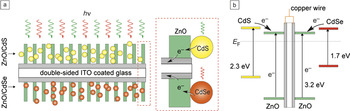
A similar recent study reported on the design and characterization of a novel double-sided CdS and CdSe QD co-sensitized ZnO nanowire array photoanode for PEC hydrogen generation.Reference Wang, Yang, Qian, Zhang and Li119 The double-sided design used dense ZnO nanowire arrays grown on an indium-tin oxide substrate followed by respective sensitization of CdS and CdSe QDs on each side (Figure 4). The photocurrent and IPCE are enhanced compared to single QD sensitized structures, which was attributed to band alignment of CdS and CdSe in the electrolyte. Moreover, in comparison to single-sided, co-sensitized layered structures, this double-sided architecture that enables direct interaction between QDs and nanowires showed improved charge collection efficiency, with a ~50% increase in IPCE at around 575 nm.
Schematic diagrams illustrating (a) the architecture and (b) the corresponding energy diagram of a double-sided CdS-ZnO-ZnO-CdSe NW arrayed photoanode. Dashed rectangles highlight the CdS-ZnO and CdSe-ZnO interfaces. ITO, indium tin oxide. Reproduced with permission from Reference Reference Wang, Yang, Qian, Zhang and Li119. ©2010, American Chemical Society. E F, Fermi energy level; h, Planck’s constant; ν, frequency.

Summary and perspective
In summary, solar hydrogen generation via photoelectrochemical water splitting is an attractive yet complex and challenging problem. Considerable progress has been made in developing various nanostructures and architectures based on metal oxides for this purpose. Some of the new strategies are encouraging for practical applications. While it will clearly take some more time before solar hydrogen generation can be implemented in large-scale commercial applications, hope is in sight that this will happen in the future. Both further experimental and theoretical studies are needed to expedite this process. With the continuing rise in energy cost and depletion of traditional energy resources, such as fossil fuels, the drive will grow to use hydrogen as a clean and alternative fuel tapping into the energy of the sun. Besides generation, storage and utilization of hydrogen also face some major challenges that need to be overcome before it can truly become a viable fuel for practical and large-scale use.
Acknowledgments
We are grateful to the financial support from the Basic Energy Sciences Division of the U.S. DOE and NSF.