Introduction
The use of quantum size effects in semiconductor nanostructures strongly stimulated research on thermoelectricity over the past decade,Reference Dresselhaus, Chen, Tang, Yang, Lee, Wang, Ren, Fleurial and Gogna1–Reference Vineis, Shakouri, Majumdar and Kanatzidis3 especially stimulated by the prediction of a significant boost in the thermoelectric (TE) figure of merit ZT = (S 2 σ T)/(κph + κel )(S is the Seebeck coefficient, σ the electrical conductivity, κ the thermal conductivity with contributions from electrons and phonons, κel and κph, and T absolute temperature) due to the transition from bulk to nanostructured materials by Hicks and Dresselhaus.Reference Hicks and Dresselhaus4,Reference Hicks and Dresselhaus5 Quantum size effects lead to a modification of the energy levels of the charge carriers and enhance their kinetic energy. Additionally, classical size effects result in an enhanced surface scattering of electrons and phonons.
Topological insulators
Recently, research interest has shifted from quantum size effects in conventional/classical semiconductors to new types of quantum materials (e.g., topological insulators [TIs], Weyl and Dirac semimetals) characterized by their nontrivial electronic topological order. Topological order is a classification of matter by the internal structure of its quantum ground state. The class of TI materials hereby represents the most relevant quantum materials for thermoelectricity. Conventional semiconductors are characterized by a bulk band structure that is constituted by a valence band and a conduction band with parabolic bands and an energy bandgap E gap < 3 eV. TE materials for near-room-temperature applications have this type of band structure, typically with E gap around 0.1 eV to 0.25 eV for high performance in the low- to mid-temperature regime. TIs also exhibit this conventional bulk band structure of a semiconductor, but feature additional topological surface states with a linear dispersion relation. As in graphene, this results in relativistic carrier transport with extremely high carrier mobility, µ, and a small effective carrier mass, m eff, which, in the ideal case, equals zero. Hence, in a primitive picture, TIs are characterized by graphene-like states on the surface of a conventional semiconductor. TIs therefore provide two different transport channels, one of graphene-like surfaces and the other of the (conventional) semiconducting bulk inner part.
Ordinary crystals are three-dimensional (3D) objects. If the crystal exhibits topological surface states completely surrounding the outer surface in all facet directions, this is called a 3D TI, also classified as a strong TI. If only certain or high-symmetry facets exhibit TI properties, the material is called a weak TI or topological crystalline insulator (TCI).
Topological surface states are protected from backscattering between equal and opposite momentum by time-reversal symmetry.Reference Seo, Roushan, Beidenkopf, Hor, Cava and Yazdani6 Therefore, the TI properties are robust, and they not only are of theoretical interest, but also contribute to the materials’ performance optimization. If, for instance, a surface of a 3D TI is oxidized, the TI states move deeper into the crystal, rather than being annihilated. Breaking of the TI state can be triggered by interaction with a magnetic dipole.Reference Buchenau, Sergelius, Wiegand, Bäßler, Zierold, Shin, Rübhausen, Gooth and Nielsch7 To probe for TI transport properties, experiments at high magnetic fields and low temperatures are performed to separate the contribution from the semiconducting bulk inner part of the material from the oscillatory behavior of the quantum transport caused by the mobile TI carriers of the surface states. By analyzing several quantum transport phenomena, such as weak antilocalization, the Aharonov–Bohm effect, Schubnikov–de Haas oscillations (SdH),Reference Gooth, Hamdou, Dorn, Zierold and Nielsch8 in addition to Fermi-level tuning, information about m eff and µ can be obtained and the linear dispersion relation proven.
The link between TI and thermoelectricity is that good TE materials are usually narrow bandgap semiconductors (E gap < 0.3 eV) and are constituted by heavy elements that suppress phonon propagation. The heavy elements also result in strong spin–orbit coupling. This is a prerequisite for the formation of topological surface states since it adds an amount of energy to the energy levels. If this amount is higher than the distance between the levels that define the bandgap, the band structure becomes inverted, and the topologically insulating state occurs.
Some of the best TE materials are also strong 3D TIs, for example, Bi2Te3, Bi2Se3, Sb2Te3,Reference Zhang, Liu, Qi, Dai, Fang and Zhang9–Reference Xu, Xu and Zhu11 and their solid solutions. Their macroscopic TE-transport properties exhibit signatures of the superposition of the surface and the bulk-transport channels. This is most clearly seen by studying transport properties in one-dimensional and two-dimensional model systems such as nanowires and thin films of Bi2Te3, Bi2Se3, and Sb2Te3.
In the last several years, substantial efforts have been invested in the development of TE Bi2Te3 nanowires and thin films to study the influence of a reduced dimension on the TE performance. The full ZT characterization of Bi2Te3 nanowires revealed values of ZT in the range of 0.02Reference Zhou, Jin, Seol, Li and Shi12 up to 0.45,Reference Chen, Chen, Lin, Ho, Lee, Chen and Harutyunyan13 considerably lower than the corresponding bulk ZT values (typically ZT > 1)Reference Snyder and Toberer14 instead of higher as was predicted due to the beneficial effect of the reduced dimension.Reference Hicks and Dresselhaus5 This is not a general characteristic of nanowires. For instance, silicon nanowires exhibit ZT values between 0.6 and 1 at room temperature,Reference Hochbaum, Chen, Delgado, Liang, Garnett, Najarian, Majumdar and Yang15,Reference Boukai, Bunimovich, Tahir-Kheli, Yu, Goddard and Heath16 and perform therewith approximately one order of magnitude better than their bulk counterparts,Reference Bux, Blair, Gogna, Lee, Chen, Dresselhaus, Kaner and Fleurial17,Reference Schierning18 mostly due to increased scattering at the rough nanowire boundaries.Reference Liu and Chen19 In InAs nanowires, a strong decrease in κ originates from increased phonon scattering at stacking faults between wurtzite and zincblende segments, accompanied by a reduction of σ attributed to a reduction of µ as a consequence of surface charges.Reference Karg, Troncale, Drechsler, Mensch, Das Kanungo, Schmid, Schmidt, Gignac, Riel and Gotsmann20,Reference Zhou, Moore, Bolinsson, Persson, Fröberg, Pettes, Kong, Rabenberg, Caroff, Stewart, Mingo, Dick, Samuelson, Linke and Shi21
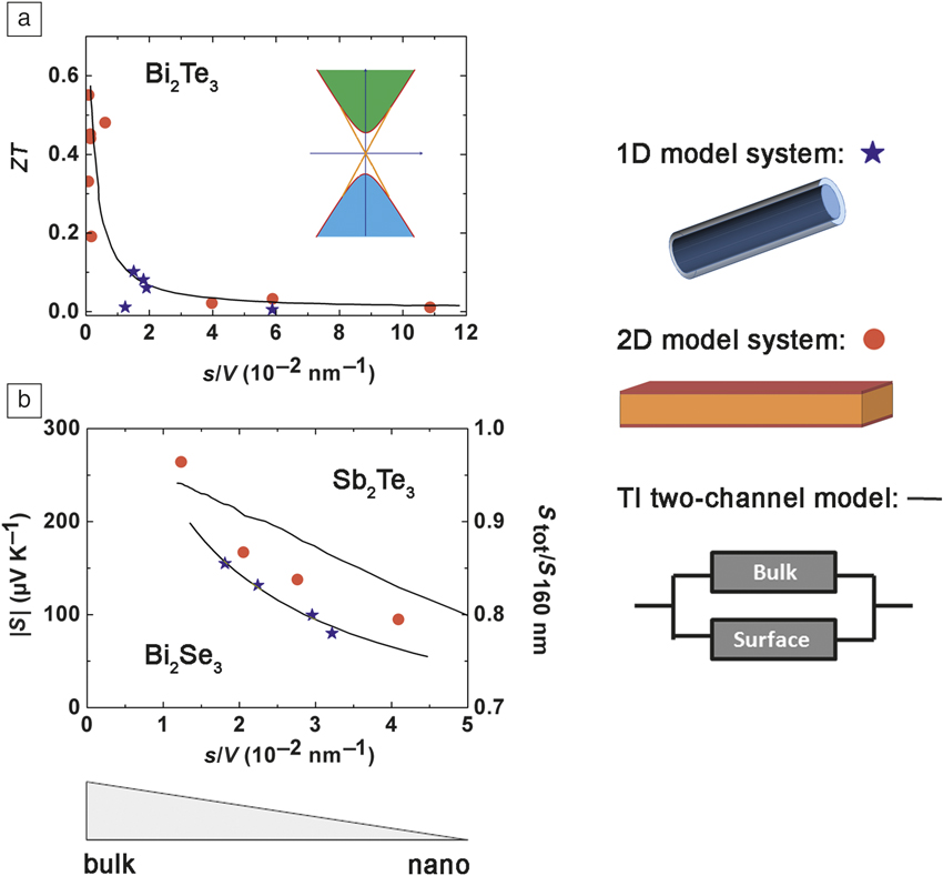
In contrast, Bi2Te3, Bi2Se3, and Sb2Te3 exhibit a more metallic character with increasing surface-to-volume (s/V) ratio, as shown in Figure 1.Reference Gooth, Gluschke, Zierold, Leijnse, Linke and Nielsch22–Reference Hinsche, Zastrow, Gooth, Pudewill, Zierold, Rittweger, Rauch, Henk, Nielsch and Mertig24 With higher s/V, a decrease in S, an increase in σ (not shown in Figure 1), and hence a decrease in ZT was evidenced. This can be interpreted to be a consequence of the surface states contributing charge carriers that exhibit superior µ carried under the regime of the linear dispersion relation. By analyzing Shubnikov-de Haas oscillations in Bi2Te3 nanowires,Reference Hamdou, Gooth, Dorn, Pippel and Nielsch23 it was found that the surface states have m c = 0.04 m 0 (the free electron mass), and µ = 21,000 cm2 V–1s–1. Shubnikov-de Haas oscillations are oscillations in the electrical resistivity of a material that occur at low temperatures in the presence of intense magnetic fields. The Shubnikov–de Haas effect is a macroscopic manifestation of the inherent quantum mechanical nature of matter. The transport properties can be described by a phenomenological model that uses two in-parallel connected transport channels for surface and bulk and also by ab initio calculations.Reference Hinsche, Zastrow, Gooth, Pudewill, Zierold, Rittweger, Rauch, Henk, Nielsch and Mertig24
Compilation of thermoelectric (TE) transport data of the 3D topological insulator (TI) TE materials Bi2Te3, Sb2Te3, and Bi2Se3 obtained using 1D and 2D model systems (nanowires and thin films, respectively) with varying surface-to-volume (s/V) ratios. (a) ZT data of Bi2Te3 nanowires and thin films show a clear trend: The smaller s/V, the higher is ZT. Inset: Sketch of the band structure of a TI. It is constituted by a bulk valence (green) and conduction (blue) band that exhibits a parabolic dispersion, and features additional topological surface states that exhibit a linear dispersion. (b) Absolute Seebeck coefficients (S) of Bi2Se3 nanowires and normalized Seebeck coefficients of Sb2Te3 thin films show more metallic behavior with higher s/V.Reference Gooth, Gluschke, Zierold, Leijnse, Linke and Nielsch22–Reference Hinsche, Zastrow, Gooth, Pudewill, Zierold, Rittweger, Rauch, Henk, Nielsch and Mertig24 Note: S tot, measured total Seebeck coefficient with contributions from the bulk and the surface states; S 160 nm, Seebeck coefficient measured using a thin film with 160-nm film thickness.

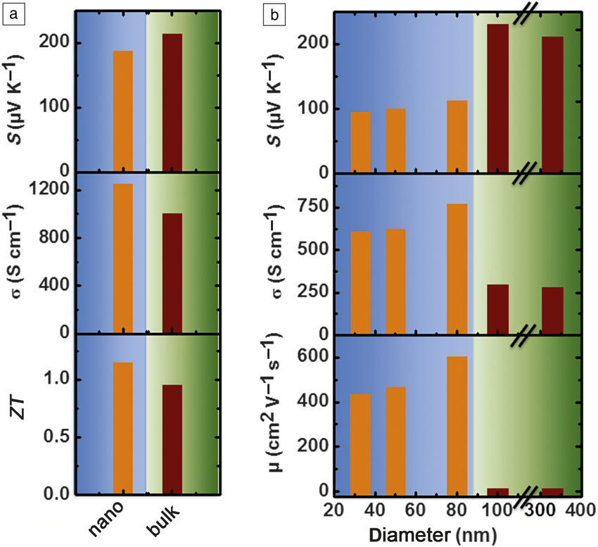
To date, the impact of topological surface states on nanograined bulk materials has not been fully understood. But some trends can be extracted. A breakthrough in TE materials development was the use of the ball-milling and hot-pressing method to achieve nanograined bulk with significantly improved ZT, compared to microstructured bulk, demonstrated for Bi2–xSbxTe3-alloys.Reference Poudel, Hao, Ma, Lan, Minnich, Yu, Yan, Wang, Muto, Vashaee, Chen, Liu, Dresselhaus, Chen and Ren25 Today, this approach has been successfully applied to all known TE materials, systematically resulting in improved ZT values. It is remarkable that in Bi2–xSbxTe3 nanograined bulk, σ is higher than that for the microstructured bulk counterpart (see Figure 2a), although often only the lower κ is discussed.
Signatures of topological insulator properties in nanograined bulk thermoelectric BiSbTe alloy and Bi2Se3. (a) Nanograined bulk of ball-milled and hot-pressed Bi2–xSbxTe3-alloy ingot resulted in an improved ZT value due to the often discussed reduction of the lattice thermal conductivity (not shown here), but also an enhancement in the electrical conductivity σ, accompanied by a reduction of the Seebeck coefficient S, despite the small grain sizes.Reference Poudel, Hao, Ma, Lan, Minnich, Yu, Yan, Wang, Muto, Vashaee, Chen, Liu, Dresselhaus, Chen and Ren25 (b) Grain-size dependence of the electrical conductivity σ and the Seebeck coefficient S of Bi2Se3 nanograined bulk also demonstrates more metallic behavior with smaller grain sizes. The analysis reveals exceptionally high values of the charge-carrier mobility μ for average grain sizes below 80 nm.Reference Sun, Li, Qin, Li, Zou, Xin, Ren, Zhang, Li and Li26

Sun and coworkersReference Sun, Li, Qin, Li, Zou, Xin, Ren, Zhang, Li and Li26 found an indication of the validity of interpreting this behavior as due to topological surface states. They analyzed the grain-size dependence of TE transport data in nanograined Bi2Se3. Due to its relatively high bandgap of 0.3 eV with an almost ideal linear electronic dispersion, called a Dirac cone, which results in exceptionally robust TI properties well above room temperature, Bi2Se3 is a perfect model TI.Reference Zhang, Liu, Qi, Dai, Fang and Zhang9,Reference Xia, Qian, Hsieh, Wray, Pal, Lin, Bansil, Grauer, Hor, Cava and Hasan27 As shown in Figure 2b, below an average grain size of 80 nm, S is lower and σ higher than in samples exhibiting an average grain size above this threshold. Most remarkable is the grain size-dependence of µ, with values of 400–600 cm2 V–1 s–1 evidenced in nanograined Bi2Se3 for grain sizes below 80 nm, compared to around 12–15 cm2 V–1 s–1 for samples with larger grain sizes. A higher σ of grain boundaries than that of the grain interiors is sometimes connected to a higher concentration of charge carriers. A higher µ of grain-boundary charge carriers is absolutely unique and can only be explained by the exceptional robustness of the surface states of strong 3D TIs that even survive the strongly distorted grain-boundary environment of a nanograined bulk.
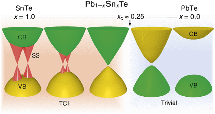
TCIs are also found in the Pb1–xSnxTe28 (Figure 3) and Pb1–xSnxSe29 material families known for their massive Dirac states in three dimensions and exceptional TE propertiesReference Heremans, Jovovic, Toberer, Saramat, Kurosaki, Charoenphakdee, Yamanaka and Snyder30,Reference Pei, Gibbs, Gloskovskii, Balke, Zeier and Snyder31 with record ZT values of 2.6, as in SnSe.Reference Zhao, Lo, Zhang, Sun, Tan, Uher, Wolverton, Dravid and Kanatzidis32 These materials can exhibit metallic surface states on high-symmetry crystal surfaces such as [111], [110], and [100] with an even number of Dirac cones.
Nontrivial electronic topology in the Pb1–xSnxTe materials family. For x = 0.4, Pb0.6Sn0.4Te is a Dirac semimetal. At the composition x c, a trivial-to-nontrivial topological quantum phase transition between the topological crystalline insulator (TCI) phase and trivial phases occurs. This is also consistent with the band inversion taking place at x c, visualized by the coloring of the valence band (VB, green in the trivial phases, yellow in the TCI phase) and conduction band (CB, yellow in the trivial phases, green in the TCI phase). Reprinted with permission from Reference Tanaka, Sato, Nakayama, Souma, Takahashi, Ren, Novak, Segawa and AndoReference 28. © 2013 Elsevier. Note: SS, surface state.

Dirac and Weyl semimetals
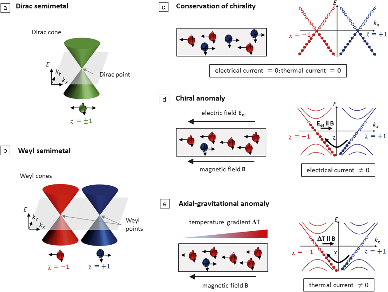
DiracReference Li, He, Lu, Zhang, Liu, Ma, Fan, Shen and Wang33–Reference Xiong, Kushwaha, Liang, Krizan, Hirschberger, Wang, Cava and Ong35 and WeylReference Shekhar, Nayak, Sun, Schmidt, Nicklas, Leermakers, Zeitler, Skourski, Wosnitza, Liu, Chen, Schnelle, Borrmann, Grin, Felser and Yan36–Reference Niemann, Gooth, Wu, Bäßler, Sergelius, Hühne, Rellinghaus, Shekhar, Süß, Schmidt, Felser, Yan and Nielsch39 semimetals, for instance, Bi1–xSbx,Reference Shin, Lee, Sasaki, Jeong, Weickert, Betts, Kim, Kim and Kim40,Reference Kim, Kim, Wang, Sasaki, Satoh, Ohnishi, Kitaura, Yang and Li41 TaAs,Reference Peng, Zhang, Shao, Lu, Zhang and Zhu42 NbP,Reference Gooth, Niemann, Meng, Grushin, Landsteiner, Gotsmann, Menges, Schmidt, Shekhar, Süß, Hühne, Rellinghaus, Felser, Yan and Nielsch43,Reference Stockert, Dos Reis, Ajeesh, Watzman, Schmidt, Shekhar, Heremans, Felser, Baenitz and Nicklas44 or Cd3As2,Reference Hosseini, Yavarishad, Alward, Kouklin and Gajdardziska-Josifovska45–Reference Zhou, Zhang, Zhang, Xiu and Yang48 are two recently discovered classes of 3D topological materials in which conduction and valence bands touch linearly close to the Fermi energy. In Dirac semimetals, both time-reversal and inversion symmetries are preserved, and the Dirac cone is degenerated (Figure 4a). Weyl states emerge when one of these symmetries is broken. The discovery of Weyl semimetals has revitalized interest in Weyl fermions that were first discovered in high-energy physics experiments. The investigation of the TE transport properties of Weyl semimetals opens the door for an advanced understanding of these exotic states of matterReference Jia, Li, Li, Shi, Liao, Yu and Wu46 in which even Ohm’s Law is fundamentally violated.Reference Shin, Lee, Sasaki, Jeong, Weickert, Betts, Kim, Kim and Kim40
Dirac and Weyl semimetals. (a) Sketch of the band structure of a Dirac and (b) of a Weyl semimetal. The cones in a Dirac semimetal are degenerated in chirality χ (direction of the charge carrier’s spin relative to its momentum). The Weyl semimetal hosts separated pairs of opposite chirality χ = –1 and χ = +1. E is the energy, and k x, k y are the momentum in the x and y directions, respectively. (c–e) show the real space scheme of the charge-carrier flow (left panels) and the associated band structure occupation (right panels). (c) Usually, the chirality is conserved. Consequently, net current flow is suppressed. However, quantum mechanical fluctuations can break the conservation law of chirality under (d) parallel magnetic B and electric fields Eel (chiral anomaly) and (e) parallel magnetic field B and temperature gradient ΔT (axial-gravitational anomaly). Under these circumstances, electrical and thermal current flow is allowed and can be tuned by the applied magnetic field.

As sketched in Figure 4b, the band touching point splits in momentum space into a pair of separated nodes (Weyl nodes) with opposite chirality, which refers to the handedness of the spin of electrons with respect to linear momentum. The conservation law of chirality dictates that the number of left-handed and right-handed electrons must always be symmetric, in other words, more electrons of one chirality than of the other cannot exist (Figure 4c). This symmetry has important consequences for the TE performance of Dirac and Weyl semimetals, because current flow is essentially the difference between the amount of left and right moving electrons of opposite chirality. Consequently, the net electrical current flow can be strongly suppressed due to the chiral conservation law. The thermopower, arising from the balance between the thermal diffusion current from hot to cold and its counter current from the accumulated charges at the cold side, is also strongly suppressed. Moreover, in both Dirac and Weyl semimetals, the energy spectrum is gapless, which results in ambipolar transport coefficientsReference Lundgren, Laurell and Fiete49 such as a small S and enhanced κel. Therefore, Dirac and Weyl semimetals are naturally poor TE materials.
However, when a magnetic field is applied in parallel to an electric field, the chiral symmetry can be violated at the quantum level.Reference Xiong, Kushwaha, Liang, Krizan, Hirschberger, Wang, Cava and Ong35,Reference Lundgren, Laurell and Fiete49–Reference Hirschberger, Kushwaha, Wang, Gibson, Liang, Belvin, Bernevig, Cava and Ong51 Applying electric and magnetic fields simultaneously to a Weyl semimetal leads to chiral charge pumping between the two branches of chiral energy levels (Landau levels), with a flow rate that is proportional to the product of the parallel magnetic and electric field components (Figure 4d). Likewise, a temperature gradient parallel to the magnetic field leads to an additional contribution that breaks the chiral symmetry (Figure 4e), originating from the so-called axial-gravitational anomaly.Reference Gooth, Niemann, Meng, Grushin, Landsteiner, Gotsmann, Menges, Schmidt, Shekhar, Süß, Hühne, Rellinghaus, Felser, Yan and Nielsch43,Reference Landsteiner, Megías and Pena-Benitez52,Reference Lucas, Davison and Sachdev53 The term “gravitational” refers to the fact that this quantum anomaly was originally thought to only occur in strong gravitational fields.Reference Witten54 For all electronic TE transport coefficients, these quantum anomalies lead to an additional topological current in parallel to the bias aligned magnetic fields,Reference Lundgren, Laurell and Fiete49,Reference Lucas, Davison and Sachdev53 increasing S, σ, and κel of a Weyl semimetal with the square of the increasing magnetic field. Consequently, the TE performance of Dirac and Weyl semimetals may be strongly enhanced when magnetic fields are present. While the existence of the chiralReference Xiong, Kushwaha, Liang, Krizan, Hirschberger, Wang, Cava and Ong35,Reference Lundgren, Laurell and Fiete49–Reference Hirschberger, Kushwaha, Wang, Gibson, Liang, Belvin, Bernevig, Cava and Ong51 and the axial-gravitational anomalyReference Gooth, Niemann, Meng, Grushin, Landsteiner, Gotsmann, Menges, Schmidt, Shekhar, Süß, Hühne, Rellinghaus, Felser, Yan and Nielsch43 have recently been experimentally confirmed, a full ZT characterization of a Weyl semimetal in a magnetic field is still missing to date.
In addition to the anomalous longitudinal transport contributions, it has been found that the linear dispersion relations in Dirac and Weyl semimetals gives rise to a large perpendicular TE voltage, the Nernst signal,Reference Liang, Gibson, Xiong, Hirschberger, Koduvayur, Cava and Ong29,Reference Sharma, Goswami and Tewari55–Reference Ferreiros, Zyuzin and Bardarson57 which can exceed their thermopower by two orders of magnitude and is significantly larger than the thermopower of traditional TE materials. Such multiterminal TE devices are of special interest, because the heat reservoirs become spatially separated from the electrical circuitry, while at the same time performing at high efficiencies. In Weyl semimetals with tilted cones, so-called Weyl type II semimetals,Reference Ferreiros, Zyuzin and Bardarson57 the Berry curvature, a local gauge field associated with the Berry phase of the topological band structure, is predicted to cause an anomalous Nernst effect even in the absence of a magnetic field, providing a platform for highly efficient TE energy converters. The Berry phase occurs in a quantum mechanical system during slow (adiabatic) traversing of a closed path in momentum space. The system does not return to its initial state, but its wave function acquires a phase factor, namely the Berry phase.
Conclusion
It seems no coincidence that many TE materials exhibit topological surface states or belong to other classes of materials with nontrivial electronic band structures. While the full spectrum of fascinating physical properties in these materials and their interplay with thermoelectricity are not yet fully understood, engineering the grain sizes and interfaces of these materials paves the path for advancing their TE performance.
Acknowledgments
This work was supported by Research Grant DFGRSF (NI616 22/1) “Contribution of topological states to the thermoelectric properties of Weyl semimetals.”

Johannes Gooth has been a joint postdoctoral fellow at the Max Planck Institute for Chemical Physics of Solids, Germany, and at Harvard University, since 2017. He studied physics at the University of Hamburg, Germany, and at Lund University, Sweden. After receiving his PhD degree from the University of Hamburg in 2014, he joined IBM Research–Zurich, Switzerland, as a postdoctoral researcher in 2015. He led the team that recently discovered the mixed axial-gravitational anomaly in Weyl semimetals. Gooth can be reached by email at johannes.gooth@cpfs.mpg.de.

Gabi Schierning joined the Leibniz Institute for Solid State and Materials Research Dresden (IFW Dresden), Germany, as head of the Department of Thermoelectric Materials in 2015. She received her PhD degree from University of Erlangen-Nuremberg, Germany, in 2005. After completing postdoctoral research, she led an independent research group at the University of Duisburg-Essen, Germany, from 2009 to 2015. She received the Award of Innovation of the State of North-Rhine Westphalia in the “young scientist” category in 2014. Schierning can be reached by email at g.schierning@ifw-dresden.de.

Claudia Felser has been director of the Max Planck Institute for Chemical Physics of Solids, Germany, since December 2011. She studied chemistry and physics at the University of Cologne, Germany, and received her PhD degree there in physical chemistry in 1994. After postdoctoral fellowships at the Max Planck Institute in Stuttgart and the CNRS in Nantes, France, she joined the University of Mainz, Germany, and became a full professor in 2003. She was a visiting scientist at Princeton University in 1999 and at Stanford University from 2009 to 2010, as well as a visiting professor at the University of Caen, France. Felser can be reached by phone at +49 351 4646-3000 or by email at claudia.felser@cpfs.mpg.de.

Kornelius Nielsch became director of the Leibniz Institute for Solid State and Materials Research Dresden (IFW Dresden), Germany, in 2015. He studied physics at the University of Duisburg, and completed his PhD degree at the Max-Planck-Institute Halle. In 2002, he was a postdoctoral associate at the Massachusetts Institute of Technology. Before he was appointed as professor for experimental physics by Hamburg University in 2006, he managed a research group in Halle. From 2009 to 2016, he coordinated the German Priority Program on Nanostructured Thermoelectrics. Nielsch can be reached by phone at +49 351 4659 102 or by email at k.nielsch@ifw-dresden.de.