I. INTRODUCTION
Ceramic thin films on plastics have long been demanded in a wide range of technologies. The greatest efforts have been made on transparent, electrically conducting oxide (TCO) thin films on plastics, which have a variety of applications in the field of flexible electronic devices. The significance of such flexible electronic devices has been addressed in the recent review articles by Reuss et al.Reference Reuss, Chalamala, Moussessian, Kane, Kumar, Zhang, Rogers, Hatalis, Temple, Moddel, Eliasson, Estes, Kunze, Handy, Harmon, Salzman, Woodall, Alam, Murthy, Jacobsen, Olivier, Markus, Campbell and Snow 1 and Sun and Rogers.Reference Sun and Rogers 2 They also stressed that many applications require the electronics to be spread over a large area, and called such electronics “macroelectronics.” Such flexible macroelectronics are attractive for a range of applications including flat-panel displays, large area radio-frequency communication devices, structural health monitors, conformal x-ray imagers, and flexible solar cells. It should be noted, however, that the applications of ceramic thin films on plastics would not be limited to the field of flexible macroelectronics, considering that ceramics have many kinds of properties that can be utilized as functions. In other words, ceramic thin films can provide the surface of plastics a variety of functions based on their optical, electrical, magnetic, dielectric, and chemical properties. Such recognition may be appreciated particularly by those who aim at replacing glass substrates by lightweight plastics.
Active functions of ceramics emerge in many cases in their crystalline states. High bulk densities or small porosities are often required for better properties. However, crystallization as well as densification is driven by atomic diffusion at high temperatures where plastics cannot survive. This is why great efforts have been made so far on “low-temperature processing” where thin films are crystallized and densified without firing. The history of such low-temperature processing goes back to 1970s,Reference Sobajima, Okaniwa, Takagi, Sugiyama and Chiba 3 – Reference Howson, Avaratsiotis, Ridge and Bishop 5 where vacuum evaporation, sputtering and ion plating were applied to the preparation of TCO thin films on plastics. Since then, a number of efforts have been made on vapor phase depositions, which include sputtering,Reference Itoyama 4 , Reference Yang, Zhang, Ma, Ma and Chen 6 chemical vapor deposition (CVD),Reference Ott and Chang 7 atomic layer deposition,Reference Latella, Triani, Zhang, Short, Bartlett and Ignat 8 , Reference Zhang, Triani and Fan 9 electron-Reference Chen, Yang and Hsueh 10 and ion-beamReference Kim 11 deposition, ion-plating,Reference Howson, Avaratsiotis, Ridge and Bishop 5 , Reference Yamamoto, Miyake, Yamada, Morizane, Arimitsu, Makino and Yamamoto 12 pulsed laser deposition,Reference Kim, Horwitz, Kushto, Kafafi and Chrisey 13 reactive plasma depositionReference Miyake, Yamada, Makino, Yamamoto and Yamamoto 14 and thermal evaporation.Reference Sobajima, Okaniwa, Takagi, Sugiyama and Chiba 3 , Reference de Carvalho, Lavareda, Fortunato, Vilarinho and Amaral 15 In such vapor phase depositions, the crystallization as well as densification of thin films may be achieved by high activities of atomic and molecular species in vapor phase as well as on substrate surface. Even in such techniques, however, posttreatments are occasionally needed to improve crystallinity; hydrothermal treatment for atomic layer-deposited titania thin films is an example.Reference Zhang, Triani and Fan 9
Wet processing is another route for realizing ceramic thin films on plastics. Compared with vapor phase depositions, the number of papers published in the literature is smaller for wet processing techniques that have been applied to the fabrication of ceramic thin films on plastics. However, wet processing is attractive because each step in the processing can be performed under the ambient pressure, and hence large-area coating can be realized without using expensive instruments. Because of such advantages, the number of papers published is now growing on wet processing for ceramic thin films on plastics.
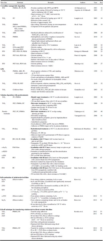
Wet processing techniques reported so far on the fabrication of ceramic thin films on plastics are reviewed in this article. Studies that have realized ceramic thin films on plastics are described, basically excluding those on thin films deposited on substrates other than plastics. The techniques are summarized in Table I, including crystalline nanoparticle deposition, liquid phase deposition (LPD), sol-gel method and chemical solution deposition (CSD). In all cases, the issue of how to crystallize and/or densify the films on plastic substrates has been focused on, and one may recognize that extraordinary efforts have been made on dealing with this issue. In the nanoparticle deposition and LPD techniques, the materials deposited on plastic substrates are crystalline, and hence firing is not needed. In sol-gel method or CSD, the amorphous precursor thin films deposited on plastics are crystallized and/or densified by posttreatments including humid vapor treatment, hot water or hydrothermal treatment, and irradiation with ultraviolet (UV) or infrared (IR) lasers. Self-combustion of CSD films has also been proposed where only heat treatment at low temperature is needed. All of these techniques are addressed in the article. Finally a transfer process that our group has proposed recently is described. Our technique is different from that of the others in that the crystallization and densification aspects are guaranteed by a firing process.
Wet processing techniques reported on fabricating ceramic thin films on plastics.

Acronyms given in the table are as follows. ABS = acrylonitrile-butadiene-styrene polymer, AcAc = acetylacetone, GPTS = 3-glycidoxypropyltrimethoxysilane, IZO = indium zinc oxide, MPTS = 3-methacryloxypropyltrimethoxysilane, PAR = polyarylate, PC = polycarbonate, PE = polyethylene, PEEK = polyetheretherketone, PEN = polyethyleneternaphthalate, PET = polyethyleneterephthalate, PI = polyimide, PMMA = polymethylmethacrylate, PTFE = polytetrafluoroethylene, PVP = polyvinylpyrrolidone, TCO = transparent and conductive oxide, and ZTO = zinc tin oxide.
II. CRYSTALLINE NANOPARTICLE DEPOSITION
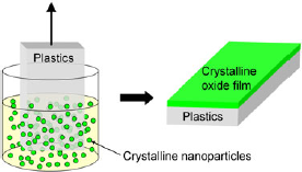
A number of papers have been published on the deposition of metal oxide nanoparticles on plastics (Fig. 1), where the nanoparticles are already crystalline before being deposited on plastic substrates, and hence there is no need to fire the films after deposition. Al-Dahoudi et al.Reference Al-Dahoudi, Bisht, Göbbert, Krajewski and Aegerter 16 and Aegerter and Al-DahoudiReference Aegerter and Al-Dahoudi 17 prepared indium tin oxide (ITO) thin films on polymethylmethacrylate (PMMA), polycarbonate (PC), polyimide (PI) and polyethylene (PE) substrates. Crystalline ITO nanoparticles about 20 nm in size were prepared by adding ethanol solution of indium chloride (InCl3) and tin (IV) chloride (SnCl4) to aqueous ammonia containing β-alanine, followed by annealing at 250 or 350 °C in a reducing atmosphere. The nanoparticles were modified by hydrolyzed 3-glycidoxypropyltrimethoxysilane (GPTS) or 3-methacryloxypropyltrimethoxysilane (MPTS). Spin- or dip coating was performed on the plastic substrates, and the deposited films were cured at 130 °C, irradiated with UV light, or treated with the combination of both. A sheet resistance as low as 1.7 kΩ/□ and a resistivity down to 9.5 × 10⁻²Ω cm were achieved for a 560-nm thick ITO film. The films consisted of loosely packed globular grains about 100 nm in size, linked together by a small strip of polymerized silanes. The thin films obtained were shown to be used as transparent and electrically conducting, antistatic, and antiglare coatings. Irradiation through a mask also allowed the formation of patterned coatings.
Schematic illustration of crystalline nanoparticle deposition for fabricating ceramic thin films on plastics.

Langlet et al.Reference Langlet, Kim, Audier, Guillard and Herrmann 18 prepared titania thin films on PC substrates by crystalline nanoparticle deposition. Anatase nanoparticles 5–20 nm in size and containing trace amounts of water and (CH3)4 NOH were prepared from ethanol solution of Ti(OC3H7 i)4 and (CH3)4 NOH through refluxing or autoclaving. Spin coating was performed on PC substrates, followed by heat treatment at temperatures up to 140 °C. The films obtained had thickness up to 350 nm, good optical transparency, and refractive index around 1.85, from which a porosity of about 30% was deduced. The anatase thin films thus prepared on PC substrates exhibited photocatalytic activity for malic acid decomposition.
Hu and YuanReference Hu and Yuan 19 prepared titania thin films on PMMA, silica-coated PMMA and silica-coated silicone rubber substrates. Anatase nanoparticles 5 nm in size were prepared by adding a Ti(OC4H9 n)4–C3H7OH solution to acidic water, followed by refluxing at 75 °C. The thin films prepared by dip coating, followed by drying at room temperature, were porous, composed of approximately 40-nm particles. Cracking occurred on PMMA substrates, which could be due to the hydrophobic nature of the substrate. On the other hand, no cracks were detected on silica-coated substrates, which was attributed to the enhanced adhesion between the films and substrates. The titania films obtained exhibited photocatalytic activities in the degradation of reactive brilliant red dye X-3B in aqueous solution.
Yang et al.Reference Yang, Han and Choy 20 also prepared photocatalytically active titania thin films on acrylonitrile-butadiene-styrene polymer (ABS) substrates. Anatase nanoparticles 5 nm in size were prepared from Ti(OC3H7 i)4 modified with acetylacetone (AcAc), which was hydrolyzed at 80 °C in the presence of nitric acid. Thin films were prepared by dip coating, where the modification by AcAc enhanced the interfacial adhesion between films and plastic substrates. Su et al.Reference Su, Wang, Wang, Fu and Weng 21 prepared anatase thin films on PMMA substrates, using colloidal anatase of ∼4 nm in crystallite size, which was prepared by a procedure similar to that of Ref. Reference Hu and Yuan19. They performed plasma pretreatment on PMMS substrates for improving the hydrophilicity and for increasing the surface roughness, which were advantageous for the effective coating. The anatase films on PMMA substrates showed natural light-induced antibacterial effects and antiadhesion of bacterial contamination. Lam et al.Reference Lam, Soetanto and Amal 22 also examined the effect of the substrate pretreatment on adhesion for anatase thin films on PC substrates, where colloidal anatase was prepared from Ti(OC4H9)4 via hydrolysis and hydrothermal treatment at 200 °C. They found that UV-C irradiation was effective in the improvement of the adhesion due to the increase in the hydroxyl and carboxyl groups on the PC substrates.
KrebsReference Krebs 23 , Reference Krebs 24 prepared ZnO thin films either on commercially available ITO-coated polyethyleneterephthalate (PET) substrates or on Ag-coated polyethylenenaphthalate (PEN) substrates. Zinc oxide (ZnO) thin films were prepared by slot-die coating using suspensions of ZnO in chlorobenzene stabilized with methoxyethoxyacetic acid. The ZnO films were demonstrated to work as the electron-transporting layer of polymer solar cells, which were fabricated by roll-to-roll process.
Königer and MünstedtReference Königer and Münstedt 25 prepared ITO coatings on PET, PEN, PI and polyetheretherketone (PEEK) substrates using nanoparticles, and studied the influence of oscillatory bending on their electrical properties. The 3-μm thick ITO coatings they prepared on PET substrates underwent annealing at 200 °C, and had a sheet resistance of 2 kΣ/□. The coatings exhibited better electrical properties under oscillatory bending than commercially available sputtered ones.
Crystalline nanoparticle deposition was also applied to gravure printing of ITO on plastic foils. Puetz and AegerterReference Puetz and Aegerter 26 prepared large-area ITO coatings and patterned ITO thin films on PET and PEN foils by gravure printing. The coatings had thicknesses from 0.2 to >1 μm and the patterns had feature sizes of the order of 100 μm. A sheet resistance down to 0.4 kΩ/□ and transmittance over 85% in the visible region were achieved. Heusing et al.Reference Heusing, de Oliveira, Kraker, Haase, Palfinger and Veith 27 also prepared ITO coatings on PET and PEN foils by gravure printing to fabricate organic photodiodes. The coatings had sheet resistance down to 1 kΩ/□ and transmittance over 80% in the visible region.
III. LIQUID PHASE DEPOSITION (LPD)
Liquid phase deposition (LPD) is a technique that utilizes the precipitation of oxides from supersaturated solutions.Reference Nagayama, Honda and Kawahara 28 – Reference Deki, Aoi, Yanagimoto, Ishii, Akamatsu, Mizuhata and Kajinami 30 The LPD process originally proposed consisted of the hydrolysis of metal fluorocomplex ions and the consumption of fluoride ions by boric acid. Shimizu et al.Reference Shimizu, Imai, Hirashima and Tsukuma 31 however, focused on the dependence of solubility of titania on pH. They deposited titania thin films on PMMA, ABS and PC substrates as well as cotton, paper and wool by immersing the substrate materials in aqueous solutions of titanium tetrafluoride (TiF4) at 25–70 °C. The thin films dried at 60 °C were rather porous, consisting of anatase particles several tens of nanometers in size, and had thickness up to 170 nm. When the substrates were relatively hydrophobic, which is the case with PMMA, ABS and PC, the precipitated anatase films had many cracks and were easily peeled off. When the substrates were hydrophilic, on the other hand, homogeneous anatase films with good adhesion were obtained, for instance, on cotton, paper and wool. The deposited anatase particles were thought to be bound to the substrates by hydrogen bonds or by bridging oxygen formed via dehydration reaction.
Ou et al.Reference Ou, Wang, Zhang, Zhang, Liu, Yan, Liu and Yang 32 prepared titania thin films on polytetrafluoroethylene (PTFE), PE and PET substrates by an LPD method. The substrates were first dipped into a hydrochloric acid solution of 3-hydroxytyramine hydrochloride and tris(hydroxymethyl) aminomethane, which resulted in the formation of 20-nm thick polydopamine coatings. The substrates were then immersed in an aqueous solution containing ammonium hexafluorotitanate [(NH4)2TiF6] and boric acid (H3BO3) at room temperature, where titania nanoparticles several nanometers in size were precipitated on the substrate surface. The polydopamine coatings allowed the formation of titania thin films even on the highly hydrophobic PTFE substrates. The films had rough surface, and had some cracks due to the lateral shrinkage during the drying process.
Goutailler et al.Reference Goutailler, Guillard, Daniele and Hubert-Pfalzgraf 33 proposed a different reaction scheme for depositing uniform titania coatings on cellulose fibers. They dipped cellulose fibers in a hexane solution of Ti(OC3H7 i)4, and added a boiling aqueous solution of N(C4H9 n)4Br as a catalyst. Cellulose fibers coated with crack-free titania thin films were obtained, where the films were composed of anatase and brookite nanocrystals. The adhesion was good due to the hydrophobic properties of the cellulose fibers.
IV. SOLUTION DEPOSITION WITH POSTTREATMENTS
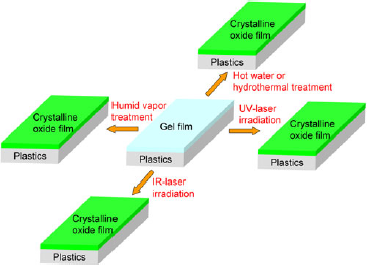
Various techniques have been reported on posttreatments for the crystallization and/or densification of precursor gel films as described below. The posttreatments include humid vapor treatment, hot water or hydrothermal treatment, and irradiation with UV or IR lasers (Fig. 2).
Techniques for converting the precursor gel films into ceramic thin films on plastics.

A. Humid vapor treatment
Imai et al.Reference Imai, Morimoto, Tominaga and Hirashima 34 , Reference Imai and Hirashima 35 reported that alkoxide-derived titania gel films on silicon wafers are crystallized by water vapor at 180 °C under autoclave conditions although the films became brittle and were easily peeled off from the substrates. They thought that the Ti–O–Ti bonds are strained and fragile in the xerogel state, and the water vapor cleaved the bonds to form Ti–OH groups, which results in the rearrangement and polycondensation to form anatase nanocrystallites.
Stimulated by Imai et al.’s work, Langlet et al.Reference Langlet, Kim, Audier and Herrmann 36 prepared anatase thin films on PC and PMMA substrates. They prepared titania gel films on plastic substrates by spin coating using a Ti(OC3H7 i)4–HCl–H2O–C2H5OH solution, followed by heat treatment at 140 °C in an autoclave that was placed in a tubular furnace and contained a small amount of an ethanol–water liquid mixture. Anatase thin films were obtained, where the crystallite size was 15–20 nm. The crystallization was accompanied by a slight increase in film thickness from 120 to 160 nm and by a noticeable increase in film porosity. The anatase films on PC substrates showed photocatalytic activity, where the porous nature rather contributed to the activity.
B. Hot water or hydrothermal treatment
Matsuda et al.Reference Matsuda, Kotani, Kogure, Tatsumisago and Minami 37 and Kotani et al.Reference Kotani, Matsuda, Tasumisago, Minami, Umezawa and Kogure 38 found that anatase nanocrystals are precipitated in alkoxide-derived titania-silica gel films when the films are immersed in hot water. They called this technique “hot-water treatment,” and prepared anatase thin films on various plastic substrates.Reference Matsuda, Matoda, Kogure, Tadanaga, Minami and Tatsumisago 39 Acid-catalyzed ethanol solutions of Si(OC2H5)4 and Ti(OC4H9 n)4 with and without polyethylene glycol (PEG) served as the coating solutions. Gel films were deposited on PET, PMMA and PC substrates by dip coating, dried at 90 °C, and then immersed into hot water of 90 °C. When a 150-nm thick gel film without PEG was immersed in the hot water, anatase nanocrystals ∼30 nm in size were precipitated on the surface of the film. When a 200-nm thick gel film with PEG was immersed, on the other hand, anatase nanocrystals ∼50 nm in size were precipitated throughout the whole of the film. The hydrolysis of the Si–O–Ti bonds, the dissolution of silica components, and the migration of hydrolyzed titania species were thought to play an important role for the nucleation and growth of anatase nanocrystals. The films were rather porous, which contributed their photocatalytic activity. The maximum thickness without cracking or peeling off was 100–200 nm on PET and PC substrates whereas the same was less than 50 nm on PMMA substrates, showing better adhesion to the former substrates.
The same group also applied the hot-water treatment to the preparation of pseudoboehmite [AlO(OH)] thin films on plastic substrates.Reference Tadanaga, Kitamuro, Matsuda and Minami 40 , Reference Yamaguchi, Tadanaga, Matsuda and Minami 41 Al(OC4H9 sec)4 was hydrolyzed in C3H7 iOH in the presence of ethylacetoacetate as a chelating agent, and dip coating was performed on PET substrates. The gel films were dried at room temperature, immersed in hot water of 60 °C, and then dried again at 60 °C. The hot-water treatment resulted in flowerlike pseudoboehmite thin films, which was thought to be formed by dissolution and reprecipitation process. A peel adhesion tape test showed that the films strongly adhered to the PET substrates. Deposition of partially hydrolyzed heptadecafluoroalkyltrimethoxysilane on the flowerlike thin films made the PET substrate surface superhydrophobic.
The flowerlike pseudoboehmite thin films were also applied as antireflective coatings for PET, PC and PMMA substrates, based on the lower density or larger porosity near the film surface.Reference Yamaguchi, Tadanaga, Matsuda and Minami 41 The Scotch-tape test showed that the adhesion was good for PET and PC substrates, but not for PMMA substrates. However, the adhesion could be improved for PMMA substrates by plasma irradiation.
Hashizume and HirashimaReference Hashizume and Hirashima 42 performed hydrothermal treatment for titania gel films on PI films. Gel films 45–200 nm in thickness were deposited on PI films using ethanol solutions of Ti(OC4H9 n)4 by spin coating, allowed to stand in air to promote hydrolysis by air moisture, and hydrothermally treated at 150 °C. The films were composed of nanometer-sized granules, and the surface was smooth but porous. They also studied the effect of the chemical modification of the PI film surface on the adhesion. The PI films were soaked in aqueous solution of sodium hydroxide (NaOH), which cleaved the imide rings, generating COOH groups on the surface. The Scotch-tape test showed that the adhesion between the hydrothermally treated titania film and the PI film is much improved by the chemical modification of the PI film.
C. Irradiation with UV lasers
Imai et al.Reference Imai, Tominaga, Hirashima, Toki and Aizawa 43 – Reference Imai, Hirashima and Awazu 45 and Asakuma et al.Reference Asakuma, Fukui, Aizawa, Toki, Imai and Hirashima 46 demonstrated that the irradiation with UV lasers induces the crystallization of indium oxide (In2O3), titania (TiO2) and lead zirconate titanate [Pb(Zr, Ti)O3] gel films. They utilized this technique to prepare ITO thin films on PET, PI, PC, and PEEK sheets.Reference Asakuma, Fukui, Toki and Imai 47 Gel films were prepared by spin coating using solutions containing In(OC4H9 sec)4, Sn(OC4H9 n)4 or Sn(OC4H9 sec)4, N, N-dimethylformamide and AcAc, followed by drying at 100 °C and exposure to an ArF excimer laser beam. The laser was operated at 1 Hz with 19 nm pulse width, and the fluence was adjusted at 20 mJ/cm2 per shot. Ten shots irradiation resulted in transparent, 95-nm thick ITO thin films 6.3 × 10⁻² and 6.2 × 10⁻²Ω cm in resistivity on PET and PI sheets, respectively. The increase in the number of shots over 10, however, resulted in an increase in resistivity, which was ascribed to the microcracks resulting from the degradation of plastic substrates caused by UV photons. Because of the damage to the plastic substrates, the ITO thin films prepared on PC and PEEK sheets did not exhibit electrical conductivity.
Very recently Kim et al.Reference Kim, Heo, Kim, Park, Yoon, Kim, Oh, Yi, Noh and Park 48 have reported a deep-UV (DUV) irradiation technique for preparing amorphous and semiconducting In2O3, indium gallium zinc oxide (IGZO), indium zinc oxide (IZO) thin films on plastic substrates. The precursor thin films were prepared by spin coating using solutions containing In(NO3)3·xH2O, Zn(CH3COO)2·2H2O, and Sn(CH3COO)4 or SnCl2 as the metal oxide sources, and CH3OC2H4OH as the solvent, followed by irradiation with DUV light from a mercury lamp under nitrogen purging. The DUV irradiation promoted the formation of metalloxane bonds as well as the film densification. Using these thin films, they fabricated thin-film-transistors on 200-μm thick polyarylate (PAR) films.
D. Irradiation with IR lasers
Königer et al.Reference Königer, Rechtenwald, Al-Naimi, Frick, Schmidt and Münstedt 49 prepared ITO thin films on PET films by means of a doctor blade using a commercially available ethanol dispersion of ITO nanoparticles approximately 100 nm in size. A plasma treatment was performed on the PET films beforehand to improve the wettability. The electrical conductivity was found to be improved by CO2-laser treatment, which was explained by a slight sinter neck formation, without thermally damaging the PET films. For a thickness of 3 μm, a sheet resistance of 0.4 kΩ/□ and a transmission in the visible range of 80% were achieved. For a bending radius of 10 mm, the sheet resistance did not exceed 1 kΩ/□ even after 300 bending cycles.
Salar Amoli et al.Reference Salar Amoli and Fathi 50 found that crystallization is promoted by irradiation with pulse Nd-YAG laser for thin films that were prepared on glass substrates using ethanol suspensions of commercially available ITO nanoparticles and were annealed at 350 °C. They also prepared ITO thin films on PC substrates using the same ITO nanoparticles that were modified by 3-methacryloxypropyltrimethoxysilane (MPTS).Reference Salar Amoli, Shokatian and Abdous 51 A 350-nm thick ITO thin film on a PC substrate had x-ray diffraction (XRD) peaks of crystalline ITO, a sheet resistance of 0.6 kΩ/□, and optical transmittance of 50–70% in the visible region. The scanning electron microscopic (SEM) image of the surface of the film revealed slight damages by the irradiation.
V. SELF-COMBUSTION OF SOLUTION-DERIVED FILMS
Kim et al.Reference Kim, Kanatzidis, Facchetti and Marks 52 have very recently presented a process that is based on self-combustion of solution-derived thin films. They chose metal nitrates as metal oxide sources, and AcAc or urea as additives. They demonstrated that the metal nitrates act as “oxidizers” and AcAc or urea acts as “fuels,” resulting in significant heat generation around 200 °C. They prepared In2O3 thin films from an AcAc-containing In(NO3)3·2.85H2O solution, and ITO thin films from a solution containing In(NO3)3·2.85H2O, tin (II) chloride (SnCl2) and ammonium nitrate (NH4NO3). A local increase in temperature due to the self-combustion allowed the In2O3 and ITO thin films to be crystallized at temperatures as low as 200 °C, where the electron mobility increased significantly. ZTO (Zn0.3Sn0.7O1.7) and IZO (In0.7Zn0.3O1.35) thin films were also prepared from solutions containing Zn(NO3)2·6H2O as zinc source with an addition of urea and AcAc, respectively. The films also exhibited a significant increase in mobility when heated up to around 200–225 °C although they remained in amorphous states. Hennek et al.Reference Hennek, Kim, Kanatzidis, Facchetti and Marks 53 the same group, also prepared amorphous indium yttrium oxide (a-IYO) thin films from AcAc-containing nitrate solutions. The films had mobility as high as 5.0 cm2/(V s) when heated at 250 °C. Kim et al.Reference Kim, Hennek, Kim, Kanatzidis, Facchetti and Marks 54 also demonstrated that the precursor solutions containing “oxidizers” and “fuels” could be used as the binders for oxide nanoparticles for preparing 60-nm thick crystalline In2O3 thin films on silicon wafers at 150 °C.
The above authors deposited their thin films on silicon wafers, not on plastic substrates. Information is awaited on the characters, performances and adhesion of the films on plastic substrates. The combination of metal nitrates and AcAc as chelating agents has been widely used for a long time by researchers working on solution deposition of oxide thin films. Therefore, the versatility of the technique, i.e., the range of thin film materials that can be prepared, is another point of interest.
VI. LIFT-OFF TECHNIQUE FOR TRANSFERRING SOLUTION-DERIVED FIRED CERAMIC THIN FILMS
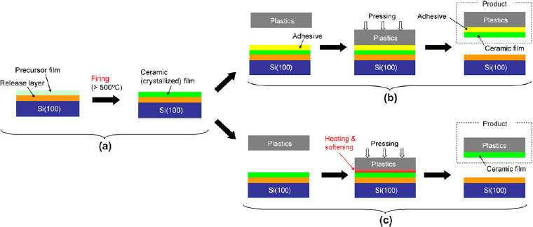
The technique we have proposed recentlyReference Kozuka, Yamano, Fukui, Uchiyama, Takahashi, Yoki and Akase 55 – Reference Kozuka, Uchiyama, Fukui and Takahashi 58 is totally different from those reported so far in that the films are fired to guarantee their crystallization and densification. The technique is based on sol-gel processing, and hence has great advantage over vapor phase depositions because all the steps are performed in the ambient atmosphere, which allows large area deposition without any specialized equipment. Figure 3 illustrates the fundamental procedure of the technique. The technique comprises (i) the deposition of gel films on thermally resistant substrates such as silicon that are coated with an organic or carbonaceous release layer, (ii) the firing of the gel films to convert them into dense, crystalline metal oxide films [Fig. 3(a)], and (iii) the transfer of the crystalline films onto plastic substrates [Figs. 3(b) and 3(c)]. Either a thermally resistant organic polymer thin film or an organic polymer-derived, thermally decomposed thin film is used as the release layer, which allows the lift-off of the fired ceramic thin film. The lift-off or transfer of the ceramic thin film can be done with [Fig. 3(b)] or without [Fig. 3(c)] the use of adhesives as will be described in this section. Although ceramics are brittle materials, the ceramic thin films prepared on the release layer surprisingly can be transferred to plastic substrates without cracking.
Transfer technique that our group has proposed. (a) Process for converting the precursor gel film into a ceramic film on a release layer on a silicon substrate. (b) Process for transferring the fired ceramic film onto a plastic substrate using an adhesive. (c) Process for transferring the fired ceramic film onto a plastic substrate without using adhesives, where the softened or molten plastics substrate acts as an adhesive.

A. Transfer process using adhesives
1. TiO2 thin films on plastics
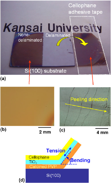
First we attempted to transfer an anatase thin film on a cellophane adhesive tape in the following manner. A coating solution of a mole ratio, polyvinylpyrrolidone (PVP):C2H5OH = 1 (monomer equivalent):15, was prepared, and dip coating was performed on an Si(100) substrate, where PVP K90 (630,000 in viscosity average molecular weight) was used. The PVP thin film thus prepared was calcined at 300 °C for 10 min, which resulted in a 2-μm thick, partially decomposed, brown-colored release layer. Then a titania gel film was prepared on the release layer from a homogeneous and transparent solution of a mole ratio, Ti(OC3H7 i)4:H2O:HNO3:C2H5OH = 1:1:0.2:20, by spin coating. The titania gel film on the release layer was heated at 5 °C/min up to 500 °C in an electric furnace, and then taken out from the furnace for cooling down to room temperature. The titania film was crystallized in anatase during firing.
The titania film was lifted off by a commercialized cellophane adhesive tape. Figure 4(a) shows the appearance of the Si(100) substrate and the cellophane adhesive tape after the transfer process where about one-half of the titania film was delaminated by the cellophane adhesive tape. The left hand side of the Si(100) substrate is colored in brown, which is the nondelaminated part. The brown color originates in the thermally decomposed release layer under the titania film. The right hand side of the Si(100) substrate is the delaminated part, where the bare substrate surface is seen. The cellophane adhesive tape has a delaminated titania film with the brown release layer on its surface. When the titania films on the release layers were fired at higher temperatures or for longer periods of time, they could not be detached from the Si(100) substrate because of the complete decomposition of the release layer.
Transfer of a fired titania thin film from a PVP-derived release layer on a silicon substrate to a cellophane adhesive tape. (a) Photograph showing the mother silicon substrate and the cellophane adhesive tape on which the fired titania thin film is transferred. Optical micrographs of (b) the non-delaminated titania film on the mother substrate, and (c) the titania film transferred to the cellophane adhesive tape. (d) Schematic illustration of the occurrence of tension and bending on the transfer process.

A serious problem encountered was the crack formation in the titania film during the transfer process. The titania film had no cracks before delamination [Fig. 4(b)], but was cracked during delamination [Fig. 4(c)] as seen in the optical micrographs. It is also seen that the cracks were aligned vertically to the peeling direction [Fig. 4(c)]. As schematically illustrated in Fig. 4(d), the titania film undergoes bending as well as in-plane tension during delamination, which could be the cause of the crack formation. The bending and in-plane tension may result from the small thickness (50 μm) of the cellophane adhesive tape.
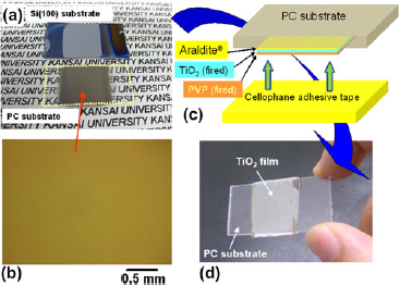
For avoiding the bending and in-plane tension, thicker plastic substrates were used instead of the cellophane adhesive tape. A commercialized epoxy resin adhesive was pasted on the fired titania film, and a PC plate (0.5 or 2 mm in thickness) was mounted on it. After two days the PC plate was detached from the Si(100) substrate, by which the fired titania film as well as the release layer was transferred to the PC plate. Crack formation during transfer process was successfully avoided by the use of such thicker plastic substrate as seen in the optical micrograph (Fig. 5). The delaminated anatase film had a brown-colored, partially decomposed release layer on its surface, which could easily be removed by a cellophane adhesive tape, leaving a colorless, transparent anatase film on the PC substrate (Fig. 5).
Transfer of a fired titania thin film from a PVP-derived release layer on a silicon substrate to a 0.5-mm thick PC substrate. (a) Photograph showing the mother silicon substrate and the PC substrate on which the fired titania thin film is transferred. (b) Optical micrograph of the titania film transferred to the PC substrate. (c) Schematic illustration showing the removal of the release layer from the titania film surface by a cellophane adhesive tape. (d) Titania film on the PC substrate after the removal of the release layer.

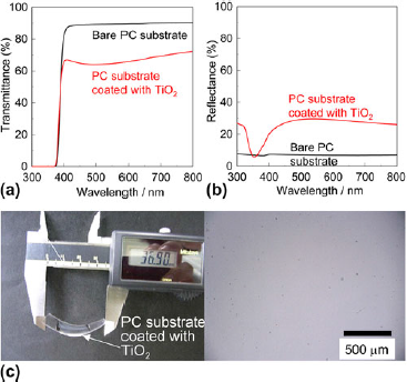
The anatase film transferred on the PC substrate had dense microstructure as was evidenced in the SEM image. The transparency of the film is demonstrated in the optical absorption spectra [Fig. 6(a)]. More importantly, the PC substrate has now high optical reflectance thanks to the anatase film as demonstrated in Fig. 6(b). The anatase film on the PC substrate could be bent to some extent without crack formation as seen in Fig. 6(c). This demonstrates the potential of the fabrication technique to be applied to high throughput roll-to-roll processes.
(a) Optical absorption spectra and (b) reflection spectra of the TiO2 film transferred on a 0.5-mm thick PC substrate using an adhesive. The absorption spectra were measured with a bare PC substrate as the reference. The spectra are also given for the bare PC substrate in (a) and (b). (c) Bending test and optical micrograph taken after the bending test for the TiO2 film on the PC substrate, where the TiO2 film is not cracked even at a radius of curvature of 20.3 mm.

2. ITO thin films on plastics
ITO thin films were prepared and transferred onto plastic substrates using adhesives in the following manner. A PI thin film was used as the release layer, which was prepared on an Si(100) substrate using a N-methyl-2-pyrrolidone solution of polyamic acid (20 mass%, U-Varnish S, Ube Industries, Ube, Japan). The as-deposited polyamic acid thin film was heated up to 450 °C under the prescribed conditions to obtain a 1.7-μm thick PI release layer.
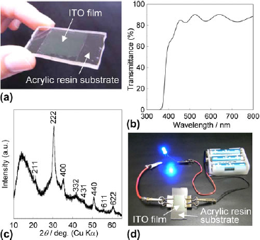
Referring to the method reported by Tomonaga and Morimoto,Reference Tomonaga and Morimoto 59 an ITO precursor solution was prepared from a solution of mole ratios, In(NO)3)3·3H2O:SnCl2·2H2O:CH3COCH2COCH3:HOCH2CH2OH:PEG 2000 (polyethylene glycol of weight average molecular weight of 2000):CH3OCH2CH(OH)CH3:CH3OH = 0.9:0.1:0.45:1.8:8.5 (monomer equivalent):6.2:17.4. The detailed preparation procedure is described in Ref. Reference Kozuka, Yamano, Fukui, Uchiyama, Takahashi, Yoki and Akase55. Spin coating was performed on the PI release layer on an Si(100) substrate, followed by firing at 500 °C for 10 min in an electric furnace. The spin coating and the firing were repeated eight times for achieving lower resistivity, resulting in a 660-nm thick ITO film. Due to the high thermal stability of PI, the release layer was not completely decomposed during such repeated firings. A commercialized epoxy resin adhesive was pasted on the fired ITO film, and a PMMA plate (3 mm in thickness) was mounted on it, followed by heating at 60 °C for 2 h. The PMMA plate was then detached from the Si(100) substrate, by which the fired ITO film as well as the PI release layer was transferred to the PMMA substrate. The PI release layer was removed from the transferred ITO film by a cellophane adhesive tape, resulting in a transparent ITO film on the PMMA substrate [Fig. 7(a)].
(a) Appearance, (b) optical absorption spectra, (c) XRD pattern, and (d) demonstration of electrical conduction for the ITO film transferred on a 3-mm thick PMMA substrate using an adhesive. The absorption spectra were measured with a bare PMMA substrate as the reference. Miller indices noted in (c) are those of ITO with bixbyite structure, and a halo observed at 2θ around 14° is originated from the PMMA substrate.

The ITO film on the PMMA substrate was transparent, [Fig. 7(b)], and was crack-free as was examined in optical micrographs and SEM images. The XRD pattern clearly showed that the film on the PMMA substrate is crystalline [Fig. 7(c)], which was achieved by the repeated firing at 500 °C before the transfer process. Figure 7(d) demonstrates the electrical conduction of the ITO film on the PMMA substrate where an LED lamp is shining by an electric current through the film. The resistivity of the ITO film on the PMMA substrate measured by four-point probe technique was 8.69 × 10⁻³Ω cm. This resistivity is not low enough compared with the values in literature, but may be lowered by optimizing the composition of the coating solution and the firing conditions.
3. Crystallographically oriented ZnO thin films on plastics
Preparation of crystallographically oriented ceramic thin films on plastic substrates is another challenge. It is known that solution-derived ZnO thin films are easily oriented crystallographically even on glass substrates.Reference Ohyama, Kozuka and Yoko 60 , Reference Ohyama, Kozuka and Yoko 61 Thereafter, we took ZnO thin films to demonstrate the possibility of the formation of oriented ceramic thin films on plastics.
Dip coating was performed on a PI release layer on an Si(100) substrate, using a homogeneous solution of molar composition, Zn(CH3COO)2·2H2O:NH2C2H4OH:CH3OC2H4OH = 1:1:16. Dip coating and calcination at 300 °C for 10 min were repeated three times, and then the film was fired at 600 °C for 5 min, resulting in a 85-nm thick, (002) oriented ZnO thin film on the release layer. A commercially available epoxy resin adhesive was pasted on the ZnO film, and a 3-mm thick PMMA plate was mounted on it, and kept in the ambient atmosphere for 2 h. The PMMA plate was then detached from the Si(100) substrate, by which the (002) oriented ZnO film was transferred to the PMMA substrate. The PI release layer on the transferred ZnO film was removed by a cellophane adhesive tape.
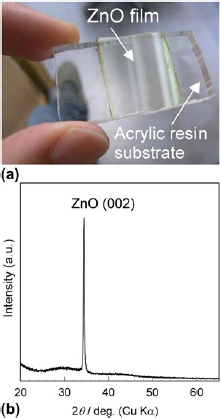
Figure 8(a) shows the ZnO film transferred onto the PMMA substrate, where transparent and reflective properties are seen. The optical micrographs and SEM images showed that the ZnO film on the PMMA substrate was crack-free. The XRD pattern measured in an ordinary θ/2θ mode shows that the (002) orientation of the ZnO film is preserved on the PMMA substrate [Fig. 8(b)].
(a) Appearance and (b) XRD pattern of the ZnO film transferred on a 3-mm thick PMMA substrate using an adhesive.

4. Patterned ZnO thin films on plastics
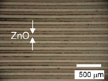
Patterned ceramic thin films can also be fabricated on plastic substrates. A diced Si(100) plate was used as the substrate, and the same procedure as that described in the previous section was used. Figure 9 shows the optical micrograph of the ZnO film thus transferred onto the PMMA substrate. Patterned ZnO films were realized on the PMMA substrate as seen in the figure.
Optical micrograph of the patterned ZnO film transferred on a PMMA substrate using an adhesive.

B. Transfer process without adhesives
1. Outline of the process
In the transfer technique described in the above section, ceramic thin films transferred onto plastic substrates have underlying adhesives. We proposed another technique where no adhesives are used, and direct bonding is realized between ceramic thin films and plastic substrates. As schematically illustrated in Fig. 3(c), the lift-off and transfer are achieved by softening or melting the surface of the plastic substrate where the softened or molten surface of plastics acts as an adhesive.
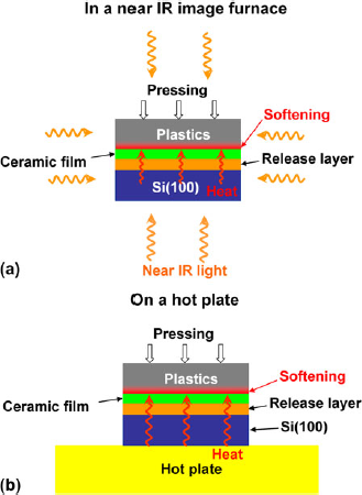
The ceramic thin film on the release layer is arranged to make contact with the plastic substrate surface so that a stack comprising plastic-substrate/ceramic-film/release-layer/Si(100)-substrate is made. Then the stack is heated either in a near-IR image furnace or from the Si(100) substrate side on a hot plate [Figs. 10(a) and 10(b)]. In a near-IR image furnace, the Si(100) substrate absorbs the near-IR lightReference Yamano and Kozuka 62 , Reference Yamano and Kozuka 63 and radiates the heat, which is transferred to the plastic substrate. When the stack is placed on a hot plate, the heat is conducted from the Si(100) substrate side to the plastic substrate. In either case, the plastics surface can be softened without softening the whole plastic substrate by optimizing the heating rate and temperature.
Schematic illustration showing the transfer process without using adhesives. (a) Softening the plastic substrate surface in a near-infrared image furnace, where the silicon substrate absorbs the near-IR light and radiates the heat, which is transferred to the plastic substrate. (b) Softening the plastic substrate surface using a hot plate, where the heat is conducted from the silicon substrate side to the plastic substrate.

2. TiO2 thin films on plastics
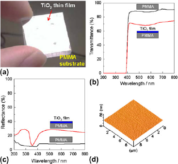
A 60-nm thick anatase thin film was prepared on a 5-mm thick PMMA substrate. The thin film was prepared from a Ti(OC3H7)4 solution by spin coating on a PI-PVP mixture release layer via heating up to 600 °C, which crystallized the film in anatase. The transfer of the anatase film to the PMMA substrate was performed in a near-IR image furnace where the PMMA/TiO2/release-layer/Si(100) stack was heated at 50 °C/min up to 170 °C. The anatase film on the PMMA substrate was obtained by peeling the PMMA substrate after cooling. The surface of the sample looks white because of the reflection of the white light by the anatase film [Fig. 11(a)]. The optical transparency and the high reflectivity of the anatase film on the PMMA substrate are demonstrated in the optical absorption and reflection spectra, respectively [Figs. 11(b) and 11(c)]. Although the transfer process appears to be severe for such a thin ceramic film to survive, the anatase film was crack-free and had flat and smooth surface. The scanning probe microscopic image of the surface of the anatase film transferred on a 5-mm thick PC substrate demonstrates high smoothness with an R a value as small as 0.62 nm [Fig. 11(d)].
(a) Appearance, (b) absorption spectra, and (c) reflection spectra of a 5-mm thick PMMA substrate coated with the 60-nm thick anatase film. The transfer was performed in the near-IR image furnace where the stack was heated up to 170 °C at 50 °C/min. The absorption spectra were measured with a bare PMMA substrate as the reference. Absorption and reflection spectra of a bare PMMA substrate are also shown. (d) Scanning probe microscopic image of the surface of the 60 nm thick anatase film transferred on a 5 mm thick PC substrate. The transfer was performed in the near-IR image furnace where the stack was heated up to 170 °C at 75 °C min−1.

3. ITO thin films on plastics
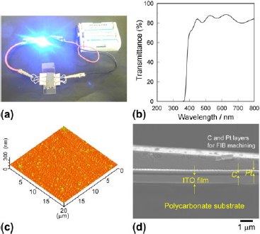
ITO thin films were also prepared on plastic substrates. The ITO thin film was prepared by spin coating on a PI-PVP release layer under the same conditions as those described in Sec. VI. A. 2. The transfer of the fired and crystallized ITO film to a 0.5-mm thick PC substrate was performed on a hot plate where the PC/ITO/release-layer/Si(100) stack was placed on a hot plate of 200 °C under a load. Figures 12(a) and 12(b) demonstrate the electrical conductivity and optical transparency of the ITO film on the PC substrate, respectively. The flat and smooth surface of the ITO film on the PC substrate was seen in the scanning probe microscopic image, where the R a value was as small as 15 nm [Fig. 12(c)]. For observing the cross section, focused ion beam (FIB) machining was performed on an ITO film that was transferred to a 5-mm thick PC substrate in a near-IR image surface, where the PC/ITO-on-Si(100) stack was heated at 75 °C/min up to 200 °C. Figure 12(d) shows the SEM image of the cross section thus made, where carbon and platinum were deposited for protecting the sample in the FIB machining. The dense microstructure is seen for the cross section of the ITO film, which was achieved by the firing process. High smoothness is confirmed for the film/substrate interface as well as for the film surface.
(a) Demonstration of electric conduction, (b) optical absorption spectra, (c) scanning probe micrograph, and (d) SEM image of the cross section fabricated by FIB for the ITO thin films transferred to PC substrates without using adhesives. The absorption spectra were measured with a bare PC substrate as the reference. The thickness of the PC substrates were 0.5 mm for (a) and (c), and 5 mm for (b) and (d). The transfer was performed on a hot plate for (a)–(c) and in a near-IR furnace for (d).

4. Patterned ITO thin films on plastics
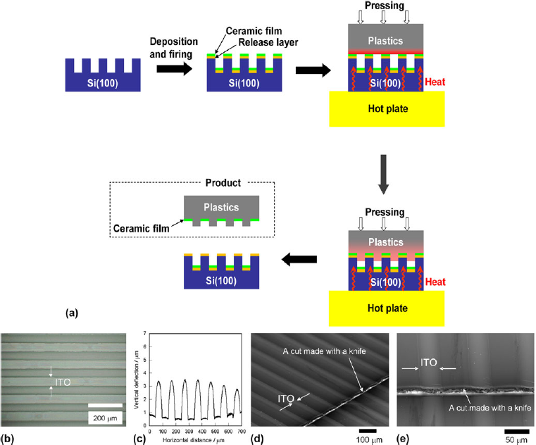
Patterned ceramic thin films can also be prepared. Figure 13(a) illustrates the process for preparing patterned ceramic thin films on plastics. A release layer and a precursor gel film are deposited by dip- and spin coating on Si(100) substrates with periodic grooves, respectively, followed by firing to convert the gel film into a ceramic film. The plastics/ceramic-film/release-layer/Si(100) stack is placed on a hot plate under a load, where the plastic substrate surface in contact with the ceramic film is molten or softened. The ceramic films in contact with the plastic substrate are transferred while those in the grooves are left, leading to the formation of patterned ceramic thin films on the plastic substrate.
(a) Process for fabricating patterned ceramic thin films on plastic substrates using a hot plate. After depositing and firing a release layer and a precursor gel film on a silicon substrate with periodic grooves, the plastics/ceramic-film/release-layer/silicon stack is placed on a hot plate under a load. The plastic substrate surface in contact with the ceramic film is molten or softened, and thus the transfer of the ceramic film onto the plastic substrate is realized. (b) Optical micrograph, (c) surface roughness profile, (d) SEM image, and (e) magnified SEM image of patterned ITO thin films transferred on a 0.5 mm thick PC substrate using a hot plate.

The optical micrograph of the patterned ITO thin films thus prepared on a PC substrate is shown in Fig. 13(b). An Si(100) substrate with periodic grooves 50 μm in width and 100 μm in depth were used as the mother substrate, and the PC/ITO/release-layer/Si(100) stack was placed on a hot plate of 200 °C under a load. ITO thin films 50 μm in width are aligned parallel on the PC substrate. In the transfer process, the softened plastics slightly intruded into the grooves of the Si(100) substrate as is schematically illustrated in Fig. 13(a). As a result, periodic PC ridges ∼3 μm in height were formed on the PC substrate as seen in the surface roughness profile shown in Fig. 13(c), where the ITO films are present in the valleys. However, such ridges and valleys are only slightly visible in the SEM pictures as shown in Figs. 13(d) and 13(e) because of the small height of the ridges compared with their width. The height of the ridges can be controlled by controlling the heating rate, temperature and load in the transfer process.
C. Transfer process using polydimethylsiloxane and comparison
Transfer or lift-off techniques with “firing” steps have been proposed recently by two other groups,Reference Qi, Jafferis, Lyons, Lee and McAlpine 64 , Reference Park, Xu, Liu, Hwang, Kang, Wang and Lee 65 although thin films are not prepared by wet processing but by radio frequency (rf) sputtering. Qi et al.Reference Qi, Jafferis, Lyons, Lee and McAlpine 64 prepared lead zirconate titanate (PZT) thin ribbons on polydimethylsiloxane (PDMS) rubbers. They prepared 500-nm thick PZT precursor thin films by radio frequency (rf) sputtering on MgO substrates that were prepatterned with resist. The resist was stripped via light sonication in acetone, and firing at 750 °C was performed to crystallize the PZT precursor films. The MgO substrates with the PZT ribbons were dipped in phosphotic acid, which undercut and loosened the ribbons, and then the PZT ribbons were transferred to PDMS plates that were brought into contact with the ribbons and quickly peeled off. Park et al.Reference Park, Xu, Liu, Hwang, Kang, Wang and Lee 65 prepared 300-nm thick barium titanate (BaTiO3) thin ribbons on Kapton films. They deposited amorphous BaTiO3 films on Pt/Ti/SiO2/Si(100) substrates by rf magnetron sputtering, followed by firing at 700 °C for crystallization. After etching the gold (Au)/BaTiO3/platinum (Pt) layers in narrow bridge patterns by an inductive coupled plasma-reactive ion etcher, the underlying Si layer was removed by anisotropic wet etching with tetramethylammonium hydroxide, which separated the Au/BaTiO3/Pt ribbons from the mother substrate. The Au/BaTiO3/Pt ribbons were transferred to a PDMS stamp, and then placed on a polyurethane (PU)-coated Kapton film. The PU was optically cured, by which the Au/BaTiO3/Pt ribbons were settled on the Kapton film, and the PDMS was peeled away.
The techniques presented by Qi et al. and Park et al. have two key points that allow the thin film transfer. One is the etching process that separates the ceramic thin ribbons and the mother substrates, and the other is the use of PDMS as stamps for lifting of the ceramic ribbons. The etching for the undercutting and film-substrate separation is possible only when the thin films have shapes of ribbons with small widths. Our process, on the other hand, uses the release layer that allows the film/Si(100) substrate separation, and hence large area ceramic thin films can be lifted off without etching of the mother substrate. And compared with the use of PDMS, our process realizes the adhesion of ceramic thin films to plastic substrates by the use of adhesives or by the melting or softening of the plastic substrate surface, which makes the lifting-off available to any kind of plastic substrates. Thus our process is more advantageous in that ceramic thin films on plastics can be realized regardless of the coating area and of the combination of plastics and ceramics. In addition, each step in the whole process can be performed in the ambient atmosphere in our process, which provides a great advantage for industrial production of ceramic thin films on plastics. Thus the technique proposed here may reform the concept and possibility of the techniques for depositing ceramic thin films on plastics that may be used as functional materials and devices in a variety of application fields.
VII. SUMMARY
Processing techniques for fabricating ceramic thin films on plastics are strongly demanded in technologies on flexible macroelectronics and by those aiming at providing the surface of lightweight, flexible plastics a variety of functions. Potential wet processing techniques for fabricating ceramic thin films on plastics have been reviewed. The techniques reviewed include crystalline nanoparticle deposition, LPD, sol-gel method and CSD. Most of the techniques have been focusing on how to crystallize and/or densify the precursor films on plastic substrates without firing, and efforts are still being made. A transfer technique that our group has proposed recently was also described, where the crystallization and densification are guaranteed by a firing process. Large area as well as patterned coating was demonstrated to be achieved on plastic substrates by the technique.
ACKNOWLEDGMENTS
This work was financially supported by MEXT (Grant-in-Aid for Scientific Research (B), and High-Tech Research Center Project for Private Universities), JST (A-STEP FS-Stage, and Highway for Promoting the Utilization of Intellectual Properties), NSG Foundation, and Expenditures for Supporting Establishment of Research Centers, Kansai University. The author thanks Ms. Mayu Yoki, Mr. Takatoshi Akase, Dr. Akihiro Yamano, Mr. Takafumi Fukui and Mr. Mitsuru Takahashi, who performed the experimental work on the transfer technique at Kansai University. The author also thanks Dr. Hiroaki Uchiyama, Kansai University for his fruitful experimental suggestions.