Introduction
Diamond is widely known as a superior material for electronics applications because of its high hardness, high thermal conductivity, and high breakdown voltage. Diamond Schottky junction diodes and field-effect transistors (FETs) are mainly being developed. In addition, diamond has unique properties for electronics applications such as extremely long spin relaxation times of point defects, negative electron affinity (NEA) of hydrogen terminated surfaces, stable exciton states at room temperature, and high conductivity for heavy doping. Using these unique properties, new types of electronic devices can be fabricated: room-temperature operating quantum devices by long spin-lattice relaxation times,Reference Gruber, Dräbenstedt, Tietz, Fleury, Wrachtrup and von Borczyskowski1,Reference Mizuochi, Makino, Kato, Takeuchi, Ogura, Okushi, Nothaft, Neumann, Gali, Jelezko, Wrachtrup and Yamasaki2 electron emission p-i-n (or p–n) diodes by NEA,Reference Koizumi, Ono and Sakai3,Reference Takeuchi, Makino, Kato, Okushi and Yamasaki4 exciton light-emitting diodes by stable excitons,Reference Koizumi, Watanabe, Hasegawa and Kanda5,Reference Makino, Kato, Ogura, Watanabe, Ri, Yamasaki and Okushi6 and high current density diodes by hopping conduction in heavily doping diamond.Reference Kato, Umezawa, Tokuda, Takeuchi, Okushi and Yamasaki7,Reference Oyama, Ri, Kato, Ogura, Makino, Takeuchi, Tokuda, Okushi and Yamasaki8 These achievements are made possible by success in high-quality diamond growth. In this article, we introduce recent progress in diamond film growth to realize electronics applications, including intrinsic and n-type doping of diamond, p-type doping of diamond, and heterostructures of diamond and other compound semiconductors.
Intrinsic and n-type doped diamond film growth
Research on diamond within the field of electronics has accelerated since the end of the 1990s when high-quality intrinsic and boron-doped p-type diamond was fabricated. High-quality diamond is homoepitaxially grown by the plasma-enhanced chemical vapor deposition (PECVD) technique on high temperature and high pressure diamond substrates. The typical growth conditions are a substrate temperature around 1000°C, pressure of 20–100 Torr, and microwave power of 200–5000 W. The source gas is hydrogen-diluted methane, and the dilution ratio is less than 1 vol%.Reference Yamanaka, Watanabe, Masai, Takeuchi, Okushi and Kjimura9–Reference Isberg, Hammersberg, Johansson, Wikström, Twitchen, Whitehead, Coe and Scarsbook16
For p-type diamond, boron as an impurity is easily incorporated into both natural and synthetic diamond by CVD without any restriction on crystal orientation. On the other hand, n-type diamond is not present in nature, and controlled n-type doping had been considered almost impossible until 1997.Reference Koizumi, Kamo, Sato, Ozaki and Inuzuka17 Among the group V elements as dopants, nitrogen was one of the candidates for n-type doping because of its similar covalent bond length (0.074 nm) to that of diamond (0.077 nm), but it forms a deep donor level ∼1.7 eV below the bottom of the conduction band due to its structural distortion from the substitutional position in the diamond lattice.
An important breakthrough was the success of P-doped n-type diamond by Koizumi et al.Reference Koizumi, Kamo, Sato, Ozaki and Inuzuka17 They experimentally demonstrated the growth of P-doped n-type diamond on (111)-oriented diamond substrates by PECVD using a mixture of PH3/CH4 (concentration: 1,000–20,000 ppm) as a dopant source and H2 gas. They carefully controlled the growth conditions to improve crystallinity and avoid undesirable impurities such as hydrogen, boron, and nitrogen at specific P-doping concentrations. Following this success, much effort was devoted to growing high-quality P-doped, n-type diamond films,Reference Kato, Futako, Yamasaki and Okushi12–Reference Kociniewski, Barjon, Pinault, Jomard, Lusson, Ballutaud, Gorochov, Laroche, Rzepka, Chevallier and Saguy15 so that nowadays, room-temperature mobility up to ∼660 cm2/Vs for a film with a phosphorus concentration of 7 × 1016 cm−3 has been achieved.Reference Katagiri, Isoya, Koizumi and Kanda18 The phosphorus donor level in diamond was experimentally estimated at ∼0.6 eV below the bottom of the conduction band.
The discovery of phosphorus doping of diamond was limited to the (111)-oriented diamond lattice structure. For actual technological applications, the growth of n-type diamond films on (001) substrates was a basic requirement because of an advantage regarding substrate size. In 2005, Kato et al. overcame this difficulty by optimizing the conditions for CVD growth, where the parameters differ significantly compared to those for (111) growth.Reference Kato, Yamasaki and Okushi19,Reference Kato, Makino, Yamasaki and Okushi20 This is a significant achievement, eliminating the restrictions on crystal orientation of n-type doping. Based on this breakthrough, the fabrication of p–n or p-i-n junctions with good diode characteristics became feasible on (001)-oriented substrates with all CVD layers, and high-efficiency excitonic emission with deep UV light at room temperature could be realized.Reference Makino, Kato, Ogura, Watanabe, Ri, Yamasaki and Okushi6
The deep dopant level of 0.6 eV for P-doping causes a serious issue for diamond electronic devices because of the small density of free carriers at room temperature (i.e., because of the high resistivity of the material). In order to decrease the resistivity, a heavy P-doping technique has been proposed.Reference Kato, Umezawa, Tokuda, Takeuchi, Okushi and Yamasaki7,Reference Oyama, Ri, Kato, Ogura, Makino, Takeuchi, Tokuda, Okushi and Yamasaki8 Since the energy levels of dopants are very deep, even in a relatively high doping regime, these levels are separated from the extended states without overlap. Also, diamond has a strong C–C bonding energy, which reduces the defect creation probability one would expect from heavy doping. This is unique to diamond, because for other compound semiconductors, the resistivity increases with an increase in doping density in the doping proximity of 1019 cm–3. For diamond, the resistivity monotonously decreases with increasing dopant density even over 1020 cm–3. The conduction mechanism changes from band conduction to hopping conduction around 1019 cm–3.Reference Oyama, Ri, Kato, Ogura, Makino, Takeuchi, Tokuda, Okushi and Yamasaki8
At room temperature, in both p-type and n-type single crystal diamond, the resistivity can be largely reduced when hopping conduction dominates a conduction system.Reference Oyama, Ri, Kato, Ogura, Makino, Takeuchi, Tokuda, Okushi and Yamasaki8,Reference Yamanaka, Watanabe, Masai, Takeuchi, Okushi and Kjimura9 Figure 1 shows the temperature dependence of resistivity of B- and P-doped diamond films (p-type, p+-type, n-type, and n+-type; + means heavy doping). The doping concentrations of these films are 1 × 1018 cm−3, 1 × 1020 cm−3, 1 × 1018 cm−3, and 8 × 1019 cm−3, respectively. For p-type and n-type films over the entire temperature range and n+-type films (8 × 1019 cm−3) in the high-temperature range (>500 K), thermally activated conduction (band conduction) has been observed originating from donor and acceptor levels of 0.6 eV and 0.37 eV from the conduction band minimum and the valence band maximum, respectively. On the other hand, the n+-type film in a low-temperature range and the p+-type film (1 × 1020 cm−3) over the entire temperature range have a weaker temperature dependence, which originates from hopping conduction. As shown in Figure 1, n+- and p+-type films have much smaller resistivity than n- and p-type films at room temperature, respectively.
Temperature dependence of resistivity of B- and P-doped diamond films (p-type, p+-type, n-type, and n+-type).Reference Oyama, Ri, Kato, Ogura, Makino, Takeuchi, Tokuda, Okushi and Yamasaki8

The film quality of diamond still continues to be improved and valency control in diamond is almost possible. It is a good time to develop high-performance diamond electronic devices.
p-type doping of diamond
Collins et al.Reference Collins and Williams21 made the first clear demonstration of p-type behavior in some rare electricity-conducting diamond crystals in 1971. Aluminum was supposed to be the main acceptor in p-type diamond,Reference Chrenko22 but it has been shown that boron is in fact the only p-type dopant that can be incorporated with high reproducibility into the diamond structure. Its activation energy of 382 meV is rather large compared to usual semiconductors, but substitutional boron behaves as a shallow level center, with the high value being consistent with the low dielectric constant and the large hole effective masses.Reference Gheeraert, Koizumi, Teraji, Kanda and Nesladek23 The covalent radii of boron (0.082 nm) and carbon (0.077 nm) are close enough to allow incorporation of boron into substitutional sites with high solubility.
The first attempts at boron doping from the gas phase were performed using diborane (B2H6), which, upon decomposition, allows an intake of boron atoms in the gas mixture and thus a possible reintroduction of these in the solid phase.Reference Fujimori, Imai and Doi24 Subsequently, other attempts at p-doping diamond from the gas phase have been initiated from various other gaseous precursors such as trimethylborate (B(OCH3)3),Reference Chen, Chen, Hong and Wang25 trimethylboron (TMB, B(CH3)3 that has a higher thermal stability compared to diborane),Reference Cifre, Puigdollers, Polo and Esteve26 and triethylbore (B(C2H5)3).Reference Haubner, Bohr and Lux27 Boron powderReference Borst and Weis28 and boron trioxide (B2O3) dissolved in ethanolReference Show, Matsukawa, Ito, Iwase and Izumi29 were also used as impurity sources. Currently, p-doping from the gas phase is done mainly using diborane and TMB. With diborane, a doping range of a few 1014 cm–3 30 up to 1022 cm–3 31 is possible in both monocrystalline and polycrystalline layers.Reference Takano, Nagao, Takenouchi, Umezawa, Sakaguchi, Tachiki and Kawarada32
Doping by ion implantation has poor efficiency, since defect recovery is very difficult both because of the high diffusion energies in diamond (requiring high annealing temperatures) and the metastable nature of diamond inducing a transformation into graphite after amorphization due to the implantation.Reference Fontaine, Uzan-Saguy, Philosoph and Kalish33
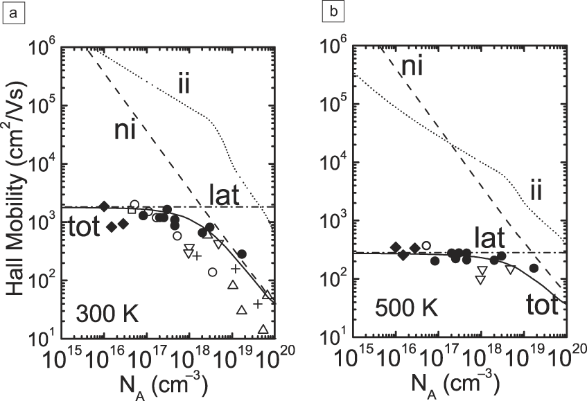
For boron concentrations lower than 2 × 1017 cm–3, the hole concentration activation energy is around 370 meV. At higher boron concentrations, the activation energy decreases near the formation of a boron impurity band, which supplies additional near-neighbor hopping conduction at low temperature. At a boron concentration of 4.5 × 1020 cm–3, metallic conduction is observed.Reference Klein, Achatz, Kacmarcik, Marcenat, Gustafsson, Marcus, Bustarret, Pernot, Omnes, Sernelius, Persson, Ferreira da Silva and Cytermann34 At room temperature, the phonon scattering mechanism governs the carrier mobility,Reference Pernot, Volpe, Omnes, Muret, Mortet, Haenen and Teraji35 leading to an intrinsic mobility of 2000 cmReference Mizuochi, Makino, Kato, Takeuchi, Ogura, Okushi, Nothaft, Neumann, Gali, Jelezko, Wrachtrup and Yamasaki2V–1s–1, as reported by several groups for high-quality lightly doped diamond films,Reference Yamanaka, Watanabe, Masai, Takeuchi, Okushi and Kjimura9,Reference Teraji, Wada, Yamamoto, Arima and Ito36,Reference Mortet, Daenen, Teraji, Lazea, Vorlicek, D’Haen, Haenen and D’Olieslaeger37 see Figure 2. In the case of doping levels larger than 1017 cm–3, the scattering induced by the ionized impurities becomes the dominant mechanism and reduces the mobility.Reference Pernot, Volpe, Omnes, Muret, Mortet, Haenen and Teraji35
Hall mobility of holes as a function of doping level in homoepitaxial diamond at (a) 300 K and (b) 500 K. The symbols indicate experimental data, and the theoretical contributions of various scattering modes are illustrated by dashed and dotted lines for the lattice (lat, acoustic, and optical phonons): a dotted line for the ionized impurities (ii) mode, and a dashed line for the neutral impurities (ni) mode.Reference Pernot, Volpe, Omnes, Muret, Mortet, Haenen and Teraji35
The large ionization energy of boron results in low carrier concentration at room temperature and consequently high resistivity. This induces a series resistance in electronic devices, and careful design reducing this resistance as much as possible is required, such as a buried heavily doped layer with metallic conductivity. This also leads to low conductance of junction FETs. In order to enhance the carrier concentration, various solutions have been explored, such as a H-terminated transistor that creates hole accumulation on the surface easily controlled by a top gate,Reference Kawarada38 or a delta-doped transistor benefitting from quantum confinement to enhance the hole mobility of a very thin metallic layer,Reference Chicot, Tran Thi, Fiori, Jomard, Gheeraert, Bustarret and Pernot39 and, more recently, a metal oxide semiconductor (MOS) transistor working in the inversion regime.Reference Chicot, Marechal, Motte, Muret, Gheeraert and Pernot40
Heterointerface
For diamond, since activation energy of dopants is larger than 0.3 eV, conductivity control is required for the operation of diamond FETs. Two major approaches have been adopted for this. The first is a diamond FET obtained using a surface conductive layer on the hydrogen-terminated diamond surface.Reference Kawarada, Aoki and Ito41 The surface is easily prepared with hydrogen plasma treatment using a microwave plasma chemical vapor deposition (MPCVD) technique and is known to provide a two-dimensional hole gas (2DHG). The 2DHG achieves a hole channel with a typical sheet carrier density of 1013 cm–2 and Hall mobility ranging from 50 to 150 cmReference Mizuochi, Makino, Kato, Takeuchi, Ogura, Okushi, Nothaft, Neumann, Gali, Jelezko, Wrachtrup and Yamasaki2/V•s. These FETs have been widely studied, and the term surface-channel FETs has been coined. Although several models have been proposed to explain the formation of the 2DHG, an exact understanding of the mechanism is still being investigated. Although surface-channel FETs have a high possibility for application in high-frequency and high-power FETs, their properties are significantly affected by their surrounding environment due to the lack of a protective layer that does not degrade the 2DHG. Thus, it has been necessary to explore passivation layers to stabilize device performance.
The second approach toward conductivity control is a diamond FET using a heavily boron-doped layer prepared with delta-doping (with thickness below 1 nm and a doping level larger than 1020 cm–3) based on the MPCVD technique.Reference Aleksov, Vescan, Kunze, Gluche, Ebert, Kohn, Bergmaier and Dollinger42 It is predicted that a delta-doped layer is required to control the FET action. Therefore, FET performance is still in the preliminary stage, and further development of the delta-doping technique is a key factor for successful fabrication of diamond FETs.
Thus, it is important to search for a new approach that provides thermally stable, high-frequency, and high-power diamond FETs. A combination of diamond and other semiconductors or dielectrics using a “heterointerface” is a possible strategy for producing such electronic devices. Miskys et al.Reference Miskys, Garrido, Nebel, Hermann, Ambacher and Stutzmann43 made the first demonstration of the AlN/diamond heterojunction diode by using a molecular beam epitaxy (MBE) technique, and an epitaxial AlN layer was obtained on the diamond substrate surface. Kueck et al.Reference Kueck, Scharpf, Ebert, Fikry, Scholz and Kohn44 reported on the effectiveness of AlN for passivating a hydrogen-terminated diamond surface. Group-III nitrides (AlN, GaN, and BN) with wide energy bandgaps are attractive materials for diamonds. Since it is difficult to grow GaN directly on diamond surfaces, AlN and BN are key materials for fabricating heterojunction FETs (HFETs). Imura et al.Reference Imura, Hayakawa, Watanabe, Liao, Koide and Amano45 demonstrated the first AlN/diamond HFET prepared by a metal organic vapor phase epitaxy technique.
The other approach to prepare a heterointerface is in dielectrics. In order to achieve high-current output FETs, strong coupling between the gate capacitance and the conductive channel is required. Simultaneously, a valence band offset, ΔE V, between the diamond and dielectric is important to accumulate holes in diamond close to the interface. Figure 3 shows a band lineup evaluated by the charge neutrality level for various semiconductors, III-nitrides, and oxides, where the zero energy equals the diamond valence band edge.Reference Mönch46,Reference Robertson47 A ΔE V value larger than 1 eV is needed to obtain the hole accumulation stage. Various gate dielectrics such as SiO2,Reference Saito, Park, Hirama, Umezawa, Satoh, Kawarada, Liu, Mitsuishi, Furuya and Okushi48 Al2O3,Reference Hirama, Sato, Harada, Yamamoto and Kasu49 CaF2,Reference Otsuka, Suzuki, Shikama, Maki and Kobayashi50 Ta2O5,Reference Cheng, Sang, Liao, Liu, Imura, Li and Koide51 HfO2,Reference Liu, Liao, Imura and Koide52 and LaAlO3Reference Liu, Liao, Imura, Oosato, Watanabe, Tanaka, Iwai and Koide53 were developed for the fabrication of MOS diodes and MOSFETs.
Energy band lineup for various semiconductors, Group III nitrides, and oxides, where the zero energy equals the diamond valence band edge. The graph is compiled using the values simulated by Mönch and Robertson.Reference Mönch46,Reference Robertson47
Figure 4 shows real charge and hole densities in diamond as a function of the electric field, which is applied to the gate dielectric. The charge density can be controlled by SiO2, Al2O3, and CaF2 and is lower than 1 μC/cmReference Mizuochi, Makino, Kato, Takeuchi, Ogura, Okushi, Nothaft, Neumann, Gali, Jelezko, Wrachtrup and Yamasaki2, which corresponds to a hole density around 1 × 1013 cm–2 at an applied electric field lower than 2 MV/cm, since the dielectric constants (k) of these dielectrics are lower than 10. A gate dielectric with k > 100 is essential to control the hole density around 1 × 1014 cm–2 reported for a hydrogen-terminated surface (see the blue dot point in Figure 4),Reference Cheng, Sang, Liao, Liu, Imura, Li and Koide51 and therefore ferroelectric materials represent a good choice of gate dielectric. The reduction in thickness of the gate dielectric to obtain a large charge density provides an increase in the leakage current that originates from carriers tunneling through the gate dielectrics. A gate insulator with higher dielectric constant (high-k) is desirable for the development of diamond FET.
Charge and hole densities in diamond as a function of electric field that is applied to gate dielectrics.Reference Cheng, Sang, Liao, Liu, Imura, Li and Koide51
Conclusion
Excellent heterointerfaces and heterojunctions are key to the successful development of high-performance diamond electron devices, and III-nitrides and high-k oxides are good candidate materials to realize these devices. Our research direction has been to search for the best gate material for diamond HFET and MOSFET.
Because diamond has superior and unique properties, we expect new types of electronic devices to emerge, which cannot be achieved using other semiconductors. To realize such electronic devices, further progress in substrate size, crystallinity, doping technique, interface control, and surface control will be important.