
Introduction
The direct conversion of solar energy to chemical fuels is a tantalizing route to store renewable energy. By employing photocatalysts to split water into H2 and O2 gas,[Reference Cook, Dogutan, Reece, Surendranath, Teets and Nocera1, Reference Walter, Warren, McKone, Boettcher, Mi, Santori and Lewis2] solar energy can be stored in H2 fuel, subsequently combined with O2 to produce water and electricity in a cycle free of CO2 emissions. A “Z-scheme”[Reference Kudo and Miseki3, Reference Li and Wu4] separates the two constituent reactions—the oxygen evolution reaction (OER) and hydrogen evolution reaction (HER)—so that they occur on separate electrodes, thus decoupling the requirements of band gap and the energy of photoexcited carriers in materials design. Typical oxide photoanodes used to drive the OER have large band gaps,[Reference Alexander, Kulesza, Rutkowska, Solarska and Augustynski5–Reference Smith, Sharp, Strandwitz and Bisquert7] and can thus absorb high-energy photons in a photoelectrochemical (PEC) device, allowing low-energy photons to pass through to the photocathode, which drives the HER.
One semiconductor with attractive light-absorption properties is Ge. In contrast to other semiconductors currently being studied, Ge has a small, indirect band gap of 0.66 eV, as well as a larger optical absorption coefficient across the visible portion of the solar spectrum and into the infrared.[Reference Sze8] Furthermore, Ge exhibits high room-temperature electron and hole mobilities of 3900 and 1900 cm2/V.s, respectively.[Reference Prince9] Density functional theory (DFT) calculations indicate that the conduction band (CB) of Ge is higher in energy than hydrogen redox,[Reference Chen and Wang10] indicating that photoexcited electrons are energetic enough to reduce H2O to evolve H2 gas. Thus, the low photovoltage cathode could harness low-energy photons (potentially combining Ge absorbers in series) coupled with a high photovoltage anode to drive solar water splitting. However, interaction with the electrolyte can lead to corrosion of the Ge surface[Reference Erdélyi and Green11] and recombination of photogenerated electron–hole pairs at surface states,[Reference Memming and Neumann12] limiting PEC activity.
We employ controlled passivation[Reference Hu, Lewis, Ager, Yang, McKone and Strandwitz13] of Ge by epitaxial growth of a wide band-gap semiconductor, SrTiO3, using oxide molecular beam epitaxy (MBE). By examining a model epitaxial film, we are able to examine charge transport through the heterostructure to yield a critical new understanding of PEC. A similar approach has recently been employed to protect a GaAs photovoltaic.[Reference Kornblum, Fenning, Faucher, Hwang, Boni, Han, Morales-Acosta, Zhu, Altman, Lee, Ahn, Walker and Shao-Horn14] Growth of SrTiO3 on Ge has previously been demonstrated for the purpose of investigating associated electrical properties,[Reference Hudait, Clavel, Zhu, Goley, Kundu, Maurya and Priya15, Reference McDaniel, Ngo, Posadas, Hu, Lu, Smith, Yu, Demkov and Ekerdt16] and we have recently measured the valence band (VB) offset between Ge and SrTiO3.[Reference Chambers, Du, Comes, Spurgeon and Sushko17] These findings support the idea that photoexcited electrons in the Ge would have a downhill path in energy to reach the SrTiO3 surface.
Here we present the first PEC measurements of the HER on a SrTiO3 (001)/p-Ge (001) heterostructure in neutral (pH 7) electrolyte. This model epitaxial system enables quantification of the abrupt interface by scanning transmission electron microscopy (STEM), as well as surface stoichiometry and speciation, both post mortem, following electrochemical cycling, and in situ using ambient pressure x-ray photoelectron spectroscopy[Reference Stoerzinger, Hong, Crumlin, Bluhm and Shao-Horn18] (AP-XPS). The Sr/Ti ratio remains similar under all conditions, suggesting that the SrTiO3 film is stable in the electrochemical environment and supporting its role as a protective cap on Ge, and the surface actively dissociates H2O to form OH groups. Surface roughness on the Ge substrate leads to pinhole defects, which hinder the efficacy of 4 nm SrTiO3 film passivation; however, a 13 nm SrTiO3 film blocks electron transport to the surface. These findings suggest that tailoring SrTiO3 electronic properties by, for example, doping may provide a promising route for Ge photocathode protection.
Experimental details
Film growth
Ga-doped p-Ge (001) substrates (AXT Inc., Freemont, CA, ρ = 0.04 Ω-cm) were prepared by wet etching procedures described elsewhere.[Reference Ponath, Posadas, Hatch and Demkov19] Following desorption of the chemically prepared oxide at ~600 °C, the surfaces were clean at the detection limit of x-ray photoelectron spectroscopy (XPS) and exhibited a (2 × 1) reconstructed surface. Epitaxial growth by oxygen-assisted MBE followed the approach outlined in Jahangir-Moghadam et al.,[Reference Jahangir-Moghadam, Ahmadi-Majlan, Shen, Droubay, Bowden, Chrysler, Su, Chambers and Ngai20] as further detailed in ref. [Reference Chambers, Du, Comes, Spurgeon and Sushko17]. An initial SrGe2 (001) (3 × 1) layer was grown at 400 °C in vacuum, followed by the growth of 3 unit cells (u.c.) amorphous SrTiO3 at ambient temperature in 4 × 10⁻⁷ Torr O2, followed by subsequent crystallization at 600 °C in vacuum. Additional layers were grown at 300 °C in O2 and annealed at up to 500 °C in vacuum to achieve better crystallinity, reaching a final thickness of 5 u.c. (2 nm), 4 nm, or 13 nm SrTiO3.
Scanning transmission electron microscopy
Cross-sectional STEM samples were prepared using an FEI Helios NanoLab Dual-Beam Focused Ion Beam (FIB) microscope and a standard lift-out procedure along the Ge [100] and [110] zone axes, with initial cuts made at 30 kV/2° and final polishing at 1 kV/3° voltage/incidence angle. High-angle annular dark field (STEM-HAADF) images were collected on a JEOL ARM-200CF microscope operating at 200 kV, with a convergence semiangle of 20.6 mrad and a collection inner semiangle ranging from 68 to 90 mrad. To minimize scan artifacts and improve signal-to-noise, drift-corrected images were prepared using the SmartAlign plugin[Reference Jones, Yang, Pennycook, Marshall, Van Aert, Browning, Castell and Nellist21]; for this, a series of ten frames at 1024 × 1024 pixels with a fast 2 µs px−1 dwell time and 90° rotation between frames was used. The frames were upsampled 3 × prior to non-rigid alignment. The inset of Fig. 1(c) was subsequently processed using a lattice-enhanced filter to improve signal-to-noise.[Reference Krivanek, Chisholm, Nicolosi, Pennycook, Corbin, Dellby, Murfitt, Own, Szilagyi, Oxley, Pantelides and Pennycook22]
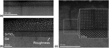
(a) Representative cross-sectional STEM-HAADF image of a 13 nm SrTiO3/p-Ge (001) heterostructure, showing the overall structure along the Ge [110] zone axis. (b) STEM-HAADF image of local Ge substrate roughness. (c) Drift-corrected STEM-HAADF image of a film discontinuity and lattice-filtered inset of an antiphase boundary between two film regions.

Electron energy loss spectroscopy (STEM-EELS) maps were collected on a Nion UltraSTEM 100MC “Hermes” microscope operating at 60 kV with a convergence semiangle of 31 mrad and a 44 mrad STEM-EELS collection angle. STEM-EELS maps were collected using 0.37 eV ch−1 dispersion, yielding an effective energy resolution of ~1.1 eV. No plural scattering correction was performed, since zero loss measurements confirm that the samples are sufficiently thin (t/λ < 0.5 inelastic mean free paths). Composition maps are presented in the supplementary information.
Photoelectrochemistry
Films were transferred directly from ultra-high vacuum (UHV) to a N2-purged glove box for PEC measurements. GaIn eutectic (Sigma, >99.99%) was scratched into the back of the Ge, and a Cu wire held in contact with the pad in a custom-built compression cell. The electrolyte was prepared from Nanopure water (18.2 MΩ-cm) from a mixture of K2HPO4 and KH2PO4 (Sigma, >99.0%) to achieve a pH of 7 and phosphate concentration of 0.1 M, and bubbled with ultra-high purity N2 gas before and during data collection. Measurements were made with a CHI-660C potentiostat by cyclic voltammetry at 20 mV/s or constant potential measurements, and voltages corrected for the electrolyte resistance between the working and reference electrodes (~95 Ω for 4 nm SrTiO3/Ge). The saturated calomel reference electrode (RE-2BP, ALS Co.) was calibrated to the reversible hydrogen electrode (RHE) scale in the same electrolyte, saturated with H2 and using Pt working and counter electrodes. A Pt counter electrode (ALS Co.) was also used for PEC measurements.
Light from a 630 nm ultra-high power LED (Prizmatix) was incident through a planar quartz window. The illuminated area of the sample was defined by the PEEK holder, and was commensurate with the area exposed to the electrolyte. The intensity of the LED at the location of the sample was measured after passing through the quartz window with a Newport 843-R power meter, and estimated to attenuate ~10% over the ~6 cm path length from water absorption.
X-ray photoelectron spectroscopy
Characterization of the films as-grown and after (photo)electrochemical cycling was performed with an Al K-α source in UHV at room temperature.
AP-XPS was collected at Beamline 9.3.2 at Lawrence Berkeley National Laboratory's (LBNL) Advanced Light Source (ALS).[Reference Grass, Karlsson, Aksoy, Lundqvist, Wannberg, Mun, Hussain and Liu23] The 5 u.c. SrTiO3/Ge was placed directly onto a ceramic heater, held in place by spring-loaded Inconel tips separated with an Al2O3 spacer, and grounded through the thermocouple. The thermocouple was pressed into a gold foil placed directly onto the sample surface and isolated from the sample holder clip with an Al2O3 spacer.
The incident photon energy (IPE) was calibrated to the Au 4f5/2 peak at 84 eV binding energy (BE). The sample was first heated to 300 °C in 100 mTorr O2 (measured by a calibrated membrane pressure gauge) and characterized. Keeping the sample at 300 °C, the chamber was evacuated to a pressure lower than 1.5 × 10⁻⁷ Torr, and 100 mTorr H2O was introduced into the chamber. The water source was prepared from deionized water (DI; Millipore, >18.2 MΩ·cm) and degassed by several freeze–pump–thaw cycles. The sample was then cooled in 100 mTorr H2O.
The O 1s spectra were deconvoluted with Gaussian–Lorentzian peaks using CasaXPS after a Shirley-type background subtraction (Table S1). The O 1s integrated area of the (bi)carbonate peak was calculated from the area of the C 1s (bi)carbonate peak using an O 1s:C 1s relative sensitivity factor, which was experimentally calibrated using the core levels of CO2 gas.[Reference Stoerzinger, Hong, Crumlin, Bluhm, Biegalski and Shao-Horn24]
Results
Figure 1 shows representative cross-sectional STEM-HAADF images that illustrate the quality of the SrTiO3 (001)/p-Ge (001) film and interface. We observe a relatively uniform film across large areas, as shown in the image of a 13 nm SrTiO3/Ge interface in Fig. 1(a). We observe no phase separation or impurities, but we do measure some substrate roughness in Fig. 1(b). This roughness is accompanied by film discontinuities and the presence of antiphase boundaries [see inset of Fig. 1(c)]. We note that the damage at the film surface (top) in this image is the result of long exposure to the electron beam and not characteristic of the film itself.
We found that this structure is highly beam sensitive at 200 kV and that exposure to the electron beam over 30–60 s was sufficient to locally amorphize the structure. To mitigate this problem, we conducted multi-frame, drift-corrected imaging using the SmartAlign plugin[Reference Jones, Yang, Pennycook, Marshall, Van Aert, Browning, Castell and Nellist21, Reference Jones, Varambhia, Beanland, Kepaptsoglou, Griffiths, Ishizuka, Azough, Freer, Ishizuka, Cherns, Ramasse, Lozano-Perez and Nellist25] to reduce the effective electron dose rate; this approach allowed us to acquire high-resolution images of the film–substrate interface without damaging the underlying structure. Figure 1(c) shows that the interface is extremely abrupt, a finding further supported by STEM-EELS maps of a related 5 u.c. SrTiO3/Ge heterostructure shown in Fig. S1; these measurements were performed at a lower 60 kV accelerating voltage to avoid excessive sample damage. Taken together, our results illustrate the uniformity, relatively good quality, and sharp interface structure that can be attained through MBE growth of these films.
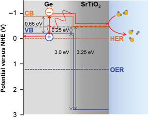
The band alignment at the SrTiO3/Ge interface is of critical importance for separation of photogenerated electrons and holes, and the transport of electrons to the surface to reduce H2O and generate H2. Previous measurement of the core levels and VB by XPS[Reference Chambers, Du, Comes, Spurgeon and Sushko17] indicate that the VB of SrTiO3 is 3.0 eV lower in energy than that of p-Ge. Coupled with the 3.25 eV band gap of SrTiO3 and the 0.66 eV band gap of Ge, the CB of SrTiO3 is found to be 0.4 eV below that of Ge. DFT band edge calculations report the Ge CB to be −0.9 V versus normal hydrogen electrode (NHE) at pH 0,[Reference Chen and Wang10] placing the CB of SrTiO3 in the heterostructure at −0.5 versus NHE (Fig. 2). This is in contrast to the CB of isolated SrTiO3, reported at −0.26 V versus NHE at pH 0.[Reference Li and Wu4] Assuming a Nernstian shift of the oxide band edges with increasing pH,[Reference Ping, Sundararaman and Goddard26] this finding then suggests that the CB of the SrTiO3/Ge heterostructures is at −0.5 V versus RHE in pH 7, resulting in photoexcited electrons being sufficiently energetic to drive the HER.
Interface band energy alignment on the NHE scale (pH = 0), obtained from the experimental measurement of VB offset in the heterostructure,[Reference Chambers, Du, Comes, Spurgeon and Sushko17] reported CB level of Ge,[Reference Chen and Wang10] and band gap of SrTiO3. For pH 7 conditions, assuming Nernstian behavior of the oxide band edges would then result in a SrTiO3 CB at −0.5 V versus RHE.

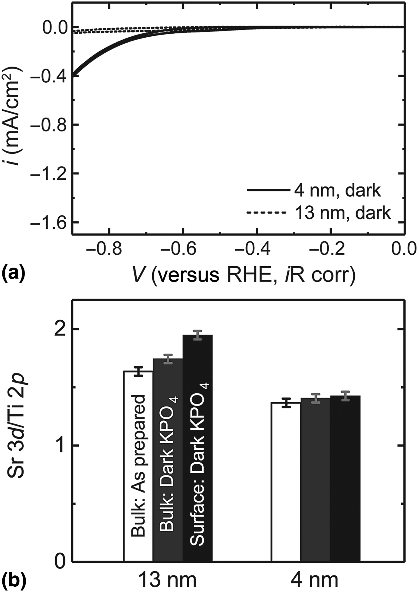
Following growth, the heterojunctions were transferred directly from UHV to a N2-purged glove box for electrochemical characterization in a custom three-electrode cell. The pH 7 phosphate-buffered electrolyte was constantly bubbled with N2 before and during measurements to minimize buildup of evolved H2 gas. Figure 3(a) compares the cyclic voltammetry for 4 and 13 nm SrTiO3 on Ge, measured initially in the dark. For the 4 nm film, cathodic current was observed commensurate with the formation of bubbles on the electrode with an onset potential ~−0.7 V versus RHE in the dark. For the 13 nm film, current was negligible within the tested window. We hypothesize that the 13 nm film acts as a blocking electrode for electrons as seen by the larger resistance measured by high-frequency impedance spectroscopy at open circuit conditions (>400 Ω, compared with <100 Ω for the 4 nm heterostructure).
(a) CV curves in dark at 20 mV/s in pH 7, 0.1 M phosphate buffer. The 13 nm SrTiO3 (dashed) acts as a blocking electrode, while the 4 nm film (solid) allows current to be passed to drive HER at high overpotentials. (b) XPS ratio of Sr 3d/Ti 2p core levels measured with hν = 1486 eV for the as-prepared heterostructure (white) and after cycling in the dark. At 90° incidence (“bulk”), the probe depth is ~7 nm, while at 20° incidence (“surface”), it is ~2 nm.

Films were then removed from the electrolyte within the purged N2 box, rinsed with DI water, dried, and returned to UHV for XPS characterization. XPS confirms no electrodeposition of Pt or other contaminants on the film (Figs. S2 and S3). The ratio of Sr 3d to Ti 2p core levels remained similar to that of the as-prepared film [Fig. 3(b)], indicating no preferential leaching of, for example, Sr occurred. This is in contrast to thermodynamic calculations of the Pourbaix diagram at pH 7, which indicate a greater stability of TiO2 with Sr cations compared with SrTiO3,[Reference Castelli, Thygesen and Jacobsen27] and suggests that additional contributors to kinetic stabilization like surface energy and functionalization play an important role. We note, however, that the ratio of the Sr 3d and Ti 2p relative to the Ge 3d for the 4 nm film (where the Ge 3d is observable due to the large probe depth of the >1400 eV kinetic energy photoelectrons) decreased after cycling (Fig. S4), suggesting the roughness of the Ge substrate may expose some pinhole defects in the SrTiO3 film, which grow with cycling.
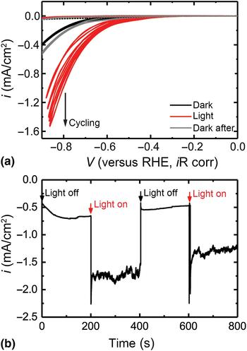
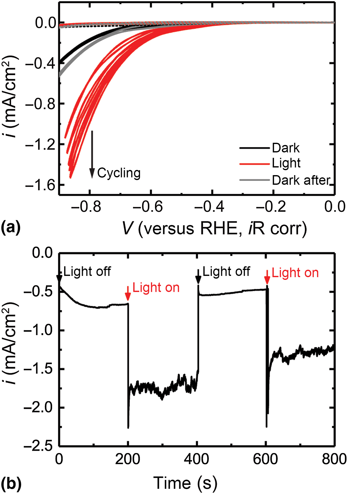
Upon illumination with an ~8 mW 630 nm LED [Fig. 4(a)], the 13 nm SrTiO3/Ge heterostructure exhibited no change in current density compared with cycling in the dark. In contrast, the 4 nm SrTiO3/Ge heterostructure exhibited a cathodic photocurrent after initially sweeping below ~−0.75 V versus RHE. The photocurrent increased with cycle number; however, the dark current remained constant before and after cycling. We hypothesize that this behavior might result from in situ generation of oxygen vacancies in the SrTiO3 film, which would facilitate electron transport to the surface. Chronoamperometry [Fig. 4(b)] illustrates the photocurrent from the 4 nm SrTiO3/Ge heterostructure directly by switching the LED on and off, in contrast to the lack of HER photocurrent from a bare Ge wafer (Fig. S5). The difference between the dark current just before 200 s and the current during illumination after 200 s (where the noise arises from the rapid generation of H2 bubbles and light scattering) gives a photocurrent of 1.1 mA/cm2 at −0.87 V versus RHE. This corresponds to an incident-photon-to-current efficiency (IPCE) of ~14%. We note that the epitaxial nature of the film on the single-crystal Ge substrate results in a roughness factor approaching unity and a highly reflective surface; thus, the photocurrent on a geometric basis and IPCE would be expected to improve greatly by introducing nanostructuring.[Reference Quan, Jang, Stoerzinger, May, Jang, Kochuveedu, Shao-Horn and Kim28] Furthermore, the high overpotential is expected to decrease substantially upon incorporation of a co-catalyst.[Reference Kwon, Choi, Hong, Andoshe, Suh, Kim, Choi, Oh, Kim and Jang29–Reference Esposito, Levin, Moffat and Talin31] Co-catalysts can improve the onset potential of photocurrent by mechanisms including passivation of surface traps, accumulation of the generated photocarriers, and aiding in charge transfer to reaction intermediates, and will be the subject of a future study.
(a) CVs at 20 mV/s in pH 7, 0.1 M phosphate buffer for the 13 nm SrTiO3 (dashed) and 4 nm SrTiO3 (solid) on Ge. Compared with polarization in the dark (black), illumination with a 630 nm LED (red) causes a photocurrent/voltage for the 4 nm film, which increases with cycling. After illumination (gray), the CV is similar to before illumination. (b) Chronoamperometry for 4 nm SrTiO3/Ge at −0.87 V versus RHE (iR corrected with average current). The dark HER current initially increases, and illumination leads to a constant −1.75 mA/cm2 current. Turning the light off returns the current to that previously measured in dark. Repeated illumination gives a similar photocurrent, however this decreases over time.
After >1 h of testing in the dark and illumination, the activity of the 4 nm SrTiO3/Ge heterostructure decreased with time. Following removal from the cell and copious rinsing to remove salt before introduction to the UHV chamber for XPS, much of the film delaminated, suggesting that pinhole defects in the 4 nm film arising from roughness of the Ge crystal grow with cycling. In contrast, the 13 nm SrTiO3 film shows comparable ratios of Sr 3d and Ti 2p and remains sufficiently thick that no Ge 3d is observed following cycling under illumination (Fig. S6). Future directions will include cation doping of thicker SrTiO3 films to ensure n-type conductivity persists over the conformal film thickness.
In order to better understand the interface between SrTiO3 and the electrolyte, we performed AP-XPS in both dry-oxidizing and humid-reducing environments. The tunable IPE at a synchrotron allows the probe depth to be tuned to the top ~1 nm of the film (hν = 690 eV, O 1s core level), and a system of differential pumping and electrostatic lensing enables the surface speciation to be probed in equilibrium with a gas.[Reference Stoerzinger, Hong, Crumlin, Bluhm and Shao-Horn18]
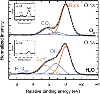
We first consider the surface at 300 °C in 100 mTorr of O2, similar to growth conditions, which minimizes carbon present from transferring the samples between growth facilities and the synchrotron (Fig. S7). Figure 5 illustrates that the O 1s spectra is dominated by bulk-coordinated oxygen of the perovskite crystal,[Reference Stoerzinger, Hong, Crumlin, Bluhm, Biegalski and Shao-Horn24] with some residual CO3 whose intensity is scaled from that of the CO3 feature in the C 1s inset. When the O2 is removed from the chamber and H2O slowly introduced, a feature increases in intensity at ~1.2 eV BE above the bulk (Fig. S8). This feature is attributed to hydroxyl, OH, formation from the dissociation of H2O on the surface.[Reference Stoerzinger, Hong, Crumlin, Bluhm, Biegalski and Shao-Horn24] In a humid environment, a feature (“Surf”) at higher BE above the bulk is notable, observed from depth profiling (Fig. S9) to be located at the surface. A feature at similar BE offsets located on the surface has been observed for (001)-oriented LaFeO3 films terminated with the “LaO” plane, but not for the “FeO2” plane.[Reference Stoerzinger, Comes, Spurgeon, Thevuthasan, Ihm, Crumlin and Chambers32] We note, however, that on the SrTiO3 surface, a small phosphorous signal (likely in the form of phosphate) was observed in humid environments (Fig. S7), and may also contribute to the signal at this intensity. Adsorption of phosphate species in humid environments may also have implications on the use and role of a PO4-containing buffer during PEC measurements.[Reference Favaro, Abdi, Lamers, Crumlin, Liu, van de Krol and Starr33]
AP-XPS performed at an incident photon energy (IPE) of hν = 690 eV at 300 °C in 100 mTorr O2 (top) or 100 mTorr H2O (bottom). The O 1s spectra is shown on a binding energy (BE) scale relative to bulk oxygen (orange), with OH (light blue), CO3 (gray, intensity determined from the shaded CO3 feature in the C 1s inset), surface oxygen (peach), and H2Ovapor (medium blue) at increasingly higher BE. Some adventitious carbon (AC, C 1s inset) remains and attenuates the spectra. Fitting parameters are given in Table S1.
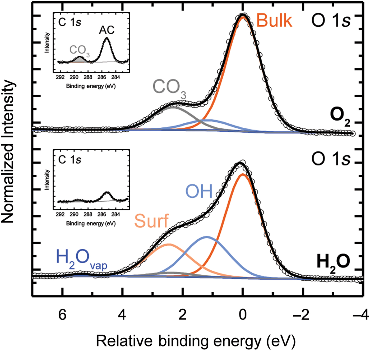
The notable dissociation of H2O on the surface of SrTiO3 to form OH species suggests that during PEC conditions in a neutral electrolyte, SrTiO3 is likely also hydroxylated. This adsorption of OH species may in turn impact band bending at the surface, of future interest for studies linking surface speciation to the driving force for charge transfer during PEC. In further consideration of the surface stoichiometry in equilibrium with gaseous environments, the ratio of Sr signal to combined Sr and Ti signals remains relatively constant across both dry-oxidizing and humid-reducing conditions, as does the distribution of Sr and Ti with depth (Fig. S10). This further supports ex situ measurements after electrochemically cycling, which indicate that Sr remains stable within the SrTiO3 film in contact with H2O at pH 7.
Conclusions
SrTiO3 was epitaxially grown on p-Ge (001) using MBE as a means to protect the surface of the Ge photoabsorber during PEC measurements in aqueous pH 7 electrolyte and maintain an energetically downhill path for photogenerated electrons to reach the solution. The band alignment between SrTiO3 and Ge is such that the photoexcited electrons can travel through a 4 nm SrTiO3 capping layer and remain sufficiently energetic to reduce H2O and evolve H2 gas in the HER. For 13 nm SrTiO3, the film behaves like a blocking electrode, with larger contact resistance and minimal current passed at similar overpotentials compared with the 4 nm film. At −0.87 V versus RHE, the IPCE for 630 nm red light is ~14%, noting that the roughness factor of the epitaxial film approaches one and notable reflective losses are not considered in calculation of the IPCE. Thus, the current density would be expected to improve with nanostructuring. Furthermore, the electrode is free of Pt or any other catalyst, and thus its probed intrinsic ability to supply photoexcited electrons to the HER is expected to substantially improve upon deposition of a co-catalyst. Some inherent roughness (on the nm scale) on the Ge surface leads to the presence of pinhole defects in the 4 nm film, resulting in corrosion and film delamination. Future directions include La doping of the SrTiO3 films to control their carrier concentration such that thicker conformal films can be epitaxially grown and maintain sufficient conductivity for charge transfer.
In situ characterization of the SrTiO3 (001)/p-Ge (001) heterostructure provides insight into the surface speciation during reaction conditions. AP-XPS was used to characterize the surface under dry-oxidizing and humid-reducing conditions. In contrast to the dry O2 environment, in a humid environment, SrTiO3 notably dissociates H2O to form OH species. This indicates that during the HER in pH 7 aqueous electrolyte, the SrTiO3 surface likely also contains some hydroxyl species. Future directions will link this speciation to the resultant surface band bending.
Supplementary material
The supplementary material for this article can be found at https://doi.org/10.1557/mrc.2018.38
Acknowledgments
AP-XPS and (photo)electrochemistry measurements and analysis were supported for K. A. S. by the Linus Pauling Distinguished Post-doctoral Fellowship at Pacific Northwest National Laboratory (PNNL LDRD 69319). Film growth and characterization was supported at PNNL by the US Department of Energy, Office of Science, Division of Materials Sciences and Engineering under Award No. 10122. The PNNL work was performed in the Environmental Molecular Sciences Laboratory (EMSL), a national science user facility sponsored by the Department of Energy's Office of Biological and Environmental Research and located at Pacific Northwest National Laboratory. PNNL is a multiprogram national laboratory operated for DOE by Battelle. STEM-EELS measurements were carried out at the SuperSTEM Laboratory, the UK National Research Facility for Advanced Electron Microscopy, which is supported by the Engineering and Physical Sciences Research Council (EPSRC). This research used resources of the Advanced Light Source, which is a DOE Office of Science User Facility under contract no. DE-AC02-05CH11231.