
I. INTRODUCTION
Implantable devices have drawn increasing attention due to their unique roles in biomedical applications, ranging from defibrillator and ventricular assist devices for heart failure Reference Bristow, Saxon, Boehmer, Krueger, Kass, De Marco, Carson, DiCarlo, DeMets, White, DeVries and Feldman1–Reference Irnich3 to drug delivery systems Reference Vallet-Regi, Balas and Arcos4,Reference LaVan, McGuire and Langer5 and tissue engineering scaffolds, Reference Williams6 to brain-machine interfaces Reference Lebedev and Nicolelis7,Reference Rousche, Pellinen, Pivin, Williams, Vetter and Kipke8 and hybrid artificial organs. Reference Colton9 Such devices can be broadly classified into two categories: one that is designed to last permanently as a hallmark of modern electronics and the other that dissolves and resorbs in the human body after operation. Most of the past developments fall into the former, whereas the latter is only available in certain passive devices, such as resorbable sutures, Reference Lendlein and Langer10 matrix for drug delivery, Reference Soppimath, Aminabhavi, Kulkarni and Rudzinski11–Reference Tobias, Lee, Engelmayr, Macaya, Bettinger and Cima13 cardiovascular stents, Reference Peuster, Wohlsein, Brugmann, Ehlerding, Seidler, Fink, Brauer, Fischer and Hausdorf14,Reference Moravej and Mantovani15 and plate-screw systems for fixation. Reference Cavusoglu, Yavuzer, Basterzi, Tuncer and Latifoglu16 However, there still exists an unaddressed need to develop high-performance electronic devices that can actively sense, actuate, and communicate in the human body. Reference Fu, Wang, Dai, Carter and Hu17–Reference Zhang, Lu, Xu and Feng19 Devices developed around year 2010 attempted to address this goal by using water-soluble materials for certain constitute components Reference Kim, Kim, Amsden, Panilaitis, Kaplan, Omenetto, Zakin and Rogers20,Reference Bettinger and Bao21 or exploring nondissolvable components on a dissolvable silk substrate. Reference Kim, Viventi, Amsden, Xiao, Vigeland, Kim, Blanco, Panilaitis, Frechette, Contreras, Kaplan, Omenetto, Huang, Hwang, Zakin, Litt and Rogers22 Although such schemes provide some utilities in disposable electronic devices or even improve contact mechanics, the nondissolvable components limit their applications in implantable devices, as a second surgical operation would still be needed for retrieval. The ideal situation remains in the case that an implantable device functions for a biologically relevant timeframe followed by a complete dissolution via resorption in the human body, eliminating the complication Reference Nery, Fernandes, Nair, Sumner, Ribas, Menon, Wang, Krahn, Morillo and Connolly23 and the need for recollection. Reference Hwang, Tao, Kim, Cheng, Song, Rill, Brenckle, Panilaitis, Won, Kim, Song, Yu, Ameen, Li, Su, Yang, Kaplan, Zakin, Slepian, Huang, Omenetto and Rogers24
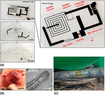
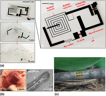
Recent developments of inorganic dissolvable devices nucleate around a realization that semiconductor grade crystalline silicon undergoes hydrolysis at physiologically relevant conditions. Reference Hwang, Tao, Kim, Cheng, Song, Rill, Brenckle, Panilaitis, Won, Kim, Song, Yu, Ameen, Li, Su, Yang, Kaplan, Zakin, Slepian, Huang, Omenetto and Rogers24 Taken together with dissolvable metals as interconnects between device components as well as biodegradable polymers for substrates, the silicon-based device provides an essential platform for future diagnostics/therapeutics. Figure 1(a) presents the dissolution sequence of a proof-of-the-concept device, which includes silicon (Si) diode, magnesium (Mg) resistor and interconnects, Mg/MgO (magnesium oxide) inductor and capacitor, and Si/MgO/Mg transistor on a silk substrate. This device was sealed in a silk package and implanted in the subdermal region of BALB/c mice. Figure 1(b) (left) revealed only faint residue in the examination after 3 weeks. At the same time, reintegration into the subdermal layers and apparent revascularization were observed. No significant inflammatory reactions were shown in the figure on the right of Fig. 1(b).
Demonstration of inorganic dissolvable electronics. (a) Sequence of optical images shows the dissolution behavior of the proof-of-concept device in deionized water. The magnified view of the device in the inset illustrates the key components that include transistors, diodes, inductors, capacitors, resistors, and interconnects on a thin silk substrate. (b) 3 weeks after implantation, only faint residue of the silk film was found at the surgical site (left) and histological section of the tissue at the surgical site (right). (A, B, and C represent subcutaneous tissue, silk film, and muscle layer, respectively.) (a)–(b): adapted with permission from Reference Hwang, Tao, Kim, Cheng, Song, Rill, Brenckle, Panilaitis, Won, Kim, Song, Yu, Ameen, Li, Su, Yang, Kaplan, Zakin, Slepian, Huang, Omenetto and RogersRef. 24. (c) An array of heterojunction bipolar transistors on a cellulose nanofibril substrate wrapped around a tree stick with a radius of 3 mm. Reprinted with permission from Reference Jung, Chang, Zhang, Yao, Zheng, Yang, Mi, Kim, Cho, Park, Jiang, Lee, Qiu, Zhou, Cai, Gong and MaRef. 33.

With the technique of transfer printing, Reference Carlson, Bowen, Huang, Nuzzo and Rogers25–Reference Kim, Carlson, Cheng, Lee, Park, Huang and Rogers30 nearly all of the bioresorbable materials can be used for dissolvable devices, enabling applications in biomedicine such as deep brain monitoring to continuously monitor the intracranial pressure and temperature, Reference Kang, Murphy, Hwang, Lee, Harburg, Krueger, Shin, Gamble, Cheng, Yu, Liu, McCall, Stephen, Ying, Kim, Park, Webb, Lee, Chung, Wie, Gujar, Vemulapalli, Kim, Lee, Cheng, Huang, Lee, Braun, Ray and Rogers31 spatiotemporal mapping of electrical activity from the cerebral cortex, Reference Yu, Kuzum, Hwang, Kim, Juul, Kim, Won, Chiang, Trumpis, Richardson, Cheng, Fang, Thompson, Bink, Talos, Seo, Lee, Kang, Kim, Lee, Huang, Jensen, Dichter, Lucas, Viventi, Litt and Rogers32 and many others. In addition to the biomedical applications, the concept that electronics dissolve after operation can also be explored for environmental sensors to avoid recollection Reference Jung, Chang, Zhang, Yao, Zheng, Yang, Mi, Kim, Cho, Park, Jiang, Lee, Qiu, Zhou, Cai, Gong and Ma33 or for consumer devices to minimize the electronic wastes generated from obsolescence. Reference Robinson34 Figure 1(c) presents an array of heterojunction bipolar transistors on a cellulose nanofibril substrate wrapped around a tree stick with a radius of 3 mm. This early demonstration shows feasibility of a sustainable and green design for high-performance flexible microwave and digital electronics. On-going efforts on reducing the use of nonrenewable materials will certainly lead to a new generation of eco-friendly devices. In addition, the physical destruction or disappearance of dissolvable electronics also creates opportunities in security-related applications. Reference Lee, Jeong, Liu, Zhang, Shi, Kang, Kim, Kim, Lee, Kim, Jang, Yin, Kim, Banks, Paik, Huang and Rogers35
This mini review with a focus on dissolvable inorganic devices is arranged in the following order. The requirement and processing consideration of materials for each device component will be introduced in Sec. II. The demonstrated applications of dissolvable electronics are discussed in Sec. III, followed by a perspective of the future developments in Sec. IV.
II. MATERIALS SELECTION
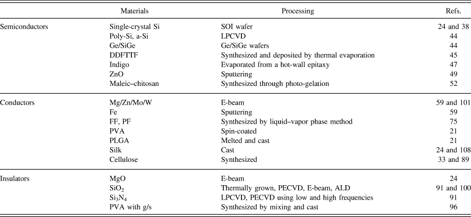
As a typical device is composed of sensor components, connecting wires, a substrate that the other components reside on, and encapsulation that protects the entire device, a natural requirement for a dissolvable electronic device is to dissolve every single component in a relevant fluidic solution. This requirement becomes particularly challenging when it comes to applications in the human body and/or the environment, where the fluidic solution has to be benign. For example, implantable devices need to function in the human body with a temperature rise ∼5 °C (Ref. Reference Xu, Lu, Seffen and Ng36) and near neutral pH levels ranging from 4.5 to 8.0 in various tissues and cellular compartments. Reference Schmaljohann37 Understanding the dissolution kinetics of each dissolvable material is essential in constructing functional devices, thus this section focuses on the dissolution behavior of each material particularly in biologically relevant conditions. The key materials and their processing methods are also summarized in Table I.
Materials and their processing methods for use in dissolvable electronics.

Poly-Si: polycrystalline silicon; a-Si: amorphous silicon; SiGe: alloy of silicon and germanium; g/s: gelatin/sucrose; LPCVD: low-pressure chemical vapor deposition; E-beam: electron beam evaporation; PECVD: plasma-enhanced chemical vapor deposition; ALD: atomic layer deposition; LPCVD: low-pressure chemical vapor deposition.
A. Semiconductors
As the industrial standard, silicon remains the most relevant material for integration and potential commercialization. In addition to the in vivo study demonstrated in Fig. 1, long-term immunologic and tissue biocompatibility were also studied in subcutaneous pockets created from sagittal skin incisions on the upper back of the mouse. Reference Hwang, Park, Cheng, Song, Kang, Yin, Kim, Omenetto, Huang, Lee and Rogers38 Implantation of test structures (silk and silicon on silk) was compared with a control that had a piece of high-density polyethylene (HDPE). Mice were monitored in a specific pathogen free facility for 5 weeks after closure of the wounds and no serious adverse events occurred during the evaluation period, suggesting that the test structures are biocompatible and nonimmunogenic.
Fast anisotropic etching of single-crystal silicon was observed in strong base solutions to fabricate a large variety of silicon structures in a controllable and reproducible manner.
Reference Seidel, Csepregi, Heuberger and Baumgartel39
For example, the etch rate of single-crystal silicon ranges from a few μm/h to a few tens of μm/h in aqueous KOH solutions with weight concentration from 10 to 60 % and temperatures from 30 to 100 °C. For aqueous KOH solutions with a concentration of 10–60 %, the silicon etch rate R was related to water concentration [H2O] and KOH concentration [KOH] by following an empirical formula
 $R = {k_0}{\left[ {{{\rm{H}}_{\rm{2}}}{\rm{O}}} \right]^4}{\left[ {{\rm{KOH}}} \right]^{1/4}{e^{−E_a/kT}}$
, where E
a is the activation energy, k is the Boltzmann constant, and T is the temperature in Kelvins. E
a and k were found to be 0.595 eV and 2480 μm/h × (mol/L)−4.25 for 〈100〉 silicon, and 0.60 eV and 4500 μm/h × (mol/L)−4.25 for 〈110〉 silicon, respectively. This empirical formula also indicates the temperature dependence follows Arrhenius scaling. Several steps are involved in the dissolution process of single-crystal silicon. Silicon surfaces with dangling bonds are first attacked by two hydroxide ions, reducing the strength of the backbonds of the surface silicon atoms. Breaking of the backbonds allows the silicon–hydroxide complex to bond to two more hydroxide ions, producing orthosilicic acid Si(OH)4. The neutral Si(OH)4 is not stable in solutions with pH levels exceeding 12, so two protons are detached, which react with two more hydroxide ions to form water molecules. The overall gross reaction of silicon in solutions with high pH levels follows:
 ${\rm{Si}} + 2{\rm{O}}{{\rm{H}}^ - } + 2{{\rm{H}}_2}{\rm{O}} \to {\rm{Si}}{{\rm{O}}_2}\left( {{\rm{OH}}} \right)_{\rm{2}}^ — + 2{{\rm{H}}_2}$
. This reaction is driven by the larger Si–O binding energy (193 kcal/mol) than that of Si–Si (78 kcal/mol).
The dissolution rate becomes however, exceptionally small when the solution is near neutral (pH ∼7). As Si(OH)4 molecules are stable in near neutral solutions, it is hypothesized that Si(OH)4 molecules can leave the solid surface by diffusion, leading to the dissolution of single-crystal silicon in near neutral solutions to follow the equilibrium:
 ${\rm{Si}} + 4{{\rm{H}}_2}{\rm{O}} \to {\rm{Si}}{\left( {{\rm{OH}}} \right)_4} + 2{{\rm{H}}_2}$
.
Reference Hwang, Tao, Kim, Cheng, Song, Rill, Brenckle, Panilaitis, Won, Kim, Song, Yu, Ameen, Li, Su, Yang, Kaplan, Zakin, Slepian, Huang, Omenetto and Rogers24,Reference Cheng, Wu, Yu, Kim-Lee, Carlson, Turner, Hwang, Huang and Rogers40
In this proposed reaction, four hydroxide ions from the reduction step are the ones that are consumed in the oxidation step, resulting in the role of hydroxide ions as catalyst. This leads to the belief that the empirical formula from Seidel et al.
Reference Seidel, Csepregi, Heuberger and Baumgartel39
may still be applicable with a different power law exponent for [OH−], which indeed captures the experimental observation for the dissolution of single-crystal silicon in near neutral solutions.
Reference Hwang, Park, Cheng, Song, Kang, Yin, Kim, Omenetto, Huang, Lee and Rogers38
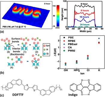
Systematic characterization of silicon dissolution can be performed on patterned silicon nanomembranes on a layer of thermal oxide. Immersion of the structure in aqueous buffer solutions allows for the measurement of the thickness and dissolution rate of silicon, as the dissolution of thermal oxide is much smaller than that of silicon [Fig. 2(a)].
Dissolution of silicon nanomembranes and other organic semiconductors. (a) Single-crystal silicon nanomembrane in the shape of a UIUC logo (100 nm thick) is characterized by a phase-sensitive microscopy technique. Line scan profiles show the dissolution sequence in phosphate buffer solution (PBS, 1M, pH 7.4, Sigma–Aldrich, USA) at physiological temperature (37 °C). Reprint with permission from Reference Hwang, Park, Edwards, Corbin, Kang, Cheng, Song, Kim, Yu, Ng, Lee, Kim, Yee, Bhaduri, Su, Omennetto, Huang, Bashir, Goddard, Popescu, Lee and RogersRef. 42. (b) (Left) Atomic configurations of each ion adsorption event obtained from density functional theory (DFT) illustrate the silicon dissolution process. (Right) Energy change computed using different functionals for different ions, indicating bonding preference of OH > HPO4 > Cl. Reprinted with permission from Reference Yin, Farimani, Min, Vishal, Lam, Lee, Aluru and RogersRef. 41. (c) Chemical structures of DDFTTF and indigo. Reprinted with permissions from Reference Bettinger and BaoRefs. 21 and Reference Irimia-Vladu, Głowacki, Troshin, Schwabegger, Leonat, Susarova, Krystal, Ullah, Kanbur and Bodea47.

Like the hydroxide ion, the other anions widely found in biological systems can also have an evident effect on the dissolution of single-crystal silicon. To understand the underlying effect of the other anions, the dissolution of silicon in solutions with different ion concentrations (chlorides and phosphates, 0.05−1 M) has also been studied at a fixed pH level (∼7.5). Reference Yin, Farimani, Min, Vishal, Lam, Lee, Aluru and Rogers41 The experiment setup is similar to the dissolution of silicon in solutions with various pH levels described above. As illustrated by density functional theory (DFT) simulations, chlorides and phosphates play a similar role as hydroxide ions in the dissolution of silicon [Fig. 2(b), left]. In near neutral solutions (e.g., pH = 7.5), the concentration of OH− (10−6 M) is much lower than that of the other anions such as chlorides and phosphates (0.05–1 M). Acting as nucleophiles to weaken the surface silicon atoms, chlorides and phosphates can also form bonds with Si. The DFT simulation finds the bonding preference is Si–OH > Si–HPO4 > Si–Cl, as confirmed by the change in energy (ΔE = E bonded − E nonbonded) between bonded and nonbonded ions for each ion [Fig. 2(b), right]. This study provides critical insights for previously reported data of silicon dissolution in various aqueous solutions, where solutions with a higher concentration of ions correspond to higher dissolution rates. Reference Hwang, Park, Cheng, Song, Kang, Yin, Kim, Omenetto, Huang, Lee and Rogers38,Reference Hwang, Park, Edwards, Corbin, Kang, Cheng, Song, Kim, Yu, Ng, Lee, Kim, Yee, Bhaduri, Su, Omennetto, Huang, Bashir, Goddard, Popescu, Lee and Rogers42 The experiment in this study also shows that even a few nanometers of silicon oxide on the silicon surface can significantly slow down the dissolution of silicon, further supporting silicon oxide as a promising candidate for encapsulation materials. After removal of the surface oxide, silicon can also go through oxidation to form silicon oxide, followed by its dissolution. But in the base solution, the DFT simulation illustrates the existence of hydroxide ions slows the formation rate of silicon oxide, thereby accelerating the silicon disassociation and dissolution.
To modulate electrical properties of silicon in semiconductor production, doping is intentionally performed to introduce impurities in the intrinsically pure silicon. An obvious reduction of the etching rate is observed in highly boron doped (p-doped) silicon due to the lack of electrons, and this etch stop phenomenon is primarily based on the electrical rather than the chemical effect of the dopant. Reference Seidel, Csepregi, Heuberger and Baumgartel43 In comparison to p-doped silicon, the reduction of the dissolution rate is much smaller in silicon doped with phosphorous (n-doped). The lack of electrons is not applicable for n-doped silicon as electrons are abundant and a different mechanism is needed to help better understand the etch stop phenomenon in n-doped silicon. Without considering the mechanism involved, the dissolution rate R doping as a function of doping concentration C can be captured by a class of equations, R doping = R i × [1 + (C/C 0) a ]−4/a , where a > 0 is a real number and C 0 is the critical doping concentration below which the dissolution R i is independent from the doping concentration C. This set of equations is also found to be applicable for the dissolution of doped silicon in near neutral solutions. Reference Hwang, Park, Edwards, Corbin, Kang, Cheng, Song, Kim, Yu, Ng, Lee, Kim, Yee, Bhaduri, Su, Omennetto, Huang, Bashir, Goddard, Popescu, Lee and Rogers42
Given their extensive use in conventional electronics, semiconducting materials such as polycrystalline silicon (poly-Si), amorphous silicon (a-Si), germanium (Ge), and alloy of silicon and germanium (SiGe) have been investigated as well.
Reference Kang, Park, Kim, Hwang, Cheng, Shin, Chung, Kim, Yin, Lee, Lee and Rogers44
The previously established chemical reaction of single-crystal silicon also applies to poly-Si and a-Si. Ge can react with water with dissolved oxygen, i.e.,
 ${\rm{Ge}} + {{\rm{O}}_2} + {{\rm{H}}_2}{\rm{O}} \to {{\rm{H}}_2}{\rm{Ge}}{{\rm{O}}_3}$
. The dissolution rate of these semiconducting materials is found to follow: a-Si > poly-Si ∼ Ge > SiGe. An in vitro cytotoxicity study further shows biocompatibility of these semiconducting materials and their dissolution products in comparison to negative control samples (no material, or high-density polyethylene), indicating their potential integration for use in dissolvable electronics. Certain organic semiconductors (e.g., DDFTTF,
Reference Bettinger and Bao21,Reference Roberts, Mannsfeld, Queraltó, Reese, Locklin, Knoll and Bao45
indigo,
Reference Irimia-Vladu, Glowacki, Voss, Bauer and Sariciftci46,Reference Irimia-Vladu, Głowacki, Troshin, Schwabegger, Leonat, Susarova, Krystal, Ullah, Kanbur and Bodea47
and etc.
Reference Irimia-Vladu, Troshin, Reisinger, Shmygleva, Kanbur, Schwabegger, Bodea, Schwödiauer, Mumyatov and Fergus48
) can also be used for devices that only require simple functions [Fig. 2(c)]. In addition, zinc oxides deposited by RF magnetron sputtering through a PI mask provide an alternative to the above discussed semiconductor materials, with expanded capabilities in energy harvesting and light emission.
Reference Dagdeviren, Hwang, Su, Kim, Cheng, Gur, Haney, Omenetto, Huang and Rogers49
Fabrication of single-crystal silicon nanomembranes (NM) follows the process of standard photolithography. Reference Liu50 Highly doped regions in Si are defined by high temperature diffusion of phosphorous and boron for n- and p- type areas in silicon-on-insulator wafers. Next, sulfur hexafluoride (SF6) gas is used in reactive ion etching (RIE) to pattern the doped Si NMs. Following a release from the wafer by removing the buried oxide in hydrofluoric acid, Si NMs can then be delivered to a target substrate (e.g., silk) via the technique of transfer printing. Layers of poly-Si and a-Si are formed on a silicon wafer from low-pressure chemical vapor deposition. Reference Kang, Park, Kim, Hwang, Cheng, Shin, Chung, Kim, Yin, Lee, Lee and Rogers44 Patterning of poly-Si and a-Si can be achieved by photolithography and RIE as for single-crystal Si. Single-crystal silicon-germanium [Si8Ge2 (100)] and germanium [Ge (100)] wafers purchased from MTI Corp. (USA) with a patterned Ti mask layer on top can be used directly for the dissolution test.
B. Conductors
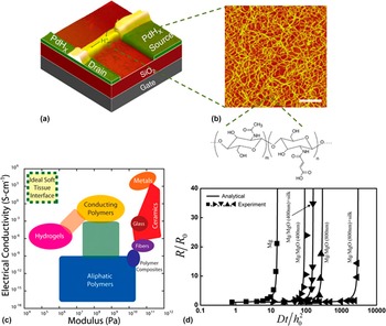
To connect electronic components, conducting materials are essential in constructing dissolvable circuits. Metals and conducting polymers represent two separate approaches. The conducting polymer has the potential to transport the neurotransmitters in their ionic form. Reference Irimia-Vladu51 As electrical signaling occurs with ions and protons rather than electrons in biological systems, the device that can monitor and control ionic/protonic currents provides an ideal interface. With a maleic–chitosan Reference Zhong, Wu, Reinhart-King and Chu52 H+-FET (field-effect transistor) shown in Figs. 3(a)–3(b), Zhong et al. Reference Zhong, Deng, Roudsari, Kapetanovic, Anantram and Rolandi53 demonstrated that an electrostatic potential applied to the gate electrode can control the flow of protonic current, from the maleic acid groups where protons dissociated to the proton conductors along the hydrated hydrogen-bond network.
Conductors for interconnects. (a) Schematic of a biopolymer protonic field-effect transistor with a maleic-chitosan nanofibre protonic channel (3.5 μm wide, 8.6 μm long, and 82 nm thick) bridging PdHx contacts of 10 μm wide (source and drain) on top of a 100 nm SiO2 gate dielectric. (b) After partial dissolution of the polysaccharide in water, AFM image is taken for the maleic-chitosan nanofibers with molecular structure shown below (m/n = 0.85, scale bar 200 nm). (a)–(b): reprinted with permission from Reference Zhong, Deng, Roudsari, Kapetanovic, Anantram and RolandiRef. 53. (c) Ashby diagram identifies the ideal material with both high electrical conductivity and high mechanical compliance in the dashed border. This region is currently inaccessible through hydrogels, polymers or their associated composites (unlabeled intermediate regions). Reprinted with permission from Reference Muskovich and BettingerRef. 56. (d) Experimental measurements (symbols) and analytical predictions (lines) of electrical resistances of Mg, Mg with MgO encapsulation layers of different thicknesses (400 and 800 nm), and Mg with MgO encapsulation layers and different silk overcoats (the percentage of the maximum crystallinity of the silk overcoats are 45 and 90% respectively). Reprinted with permission from Reference Li, Cheng, Su, Hwang, Yin, Tao, Brenckle, Kim, Omenetto, Rogers and HuangRef. 64.

In comparison to conducting polymers, Reference Zelikin, Lynn, Farhadi, Martin, Shastri and Langer54,Reference Rivers, Hudson and Schmidt55 metals are of particular interest due to their low resistivity, robustness, and widely adopted use in commercial devices. Of course, there is an unmet need to develop ideal materials with simultaneous properties of high electrical conductivity and high compliance [Figs. 3(c)] Reference Muskovich and Bettinger56 Without this type of new materials available at this time, the focus of the following subsection is placed on the metal materials that are essential for biological functions. With a recommended daily intake value ranging from 0.05 mm/day to 400 mm/day, Reference Trumbo, Yates, Schlicker and Poos57,Reference Zheng, Gu and Witte58 thin film forms of magnesium (Mg), zinc (Zn), iron (Fe), and molybdenum (Mo) were selected for study due to their biocompatibility. Reference Zheng, Gu and Witte58,Reference Yin, Cheng, Mao, Haasch, Liu, Xie, Hwang, Jain, Kang, Su, Li, Huang and Rogers59 Tungsten (W) was also included in the study, as published data indicate that W dissolves in physiological solutions with no obvious adverse effects, Reference Anik and Osseo-Asare60 though less comprehensive study of biocompatibility is reported. It is important to note that degradation of pure Mg involves generation of hydrogen gas or other gas molecules. The formed gas pocket is detrimental to the local tissues, Reference Song and Song61 which has motivated the use of Mg alloys. Reference Li, Gu, Lou and Zheng62 Thin film traces were selected for rapid rate of dissolution and favorable mechanics in bending deformation. The dissolution behavior of thin film can be quite different from that of bulk form, as grain size and pinholes as well as other factors can have dominating effects. Reference Revie and Uhlig63 The study on electrical resistance, morphology, and surface chemistry indicates a two-stage dissolution, where a fast degradation of the metal is followed by a slow dissolution of residue oxides. In comparison to W/Mo/Fe, Mg/Zn as well as AZ31B Mg alloy dissolves much faster. The residue oxide may take one week to several months to dissolve or may even be insoluble.
To provide physical insight and quantitative analysis of experimental observations, a model of reactive diffusion has been developed.
Reference Li, Cheng, Su, Hwang, Yin, Tao, Brenckle, Kim, Omenetto, Rogers and Huang64
Unlike the dissolution of single-crystal silicon where the reaction only happens at the surface, the diffusion of water and/or solution molecules cannot be ignored for porous metal materials. These molecules diffuse inside the metal traces and react with the surrounding metal material along the thickness direction. This phenomenon becomes more evident for samples with pinholes or as porosity increases after the initial reaction. The model of reactive diffusion takes diffusion into consideration and accounts for the effective area that is in reaction. Because the initial thickness of the metal traces is much smaller than their width and length, a one-dimensional (1-D) model is sufficient to capture the experimental observations. The model first calculates the concentration w(y, t) of solution molecules (e.g., water) at each location y as a function of time t. This result is obtained by analytically solving the reactive diffusion equation,
Reference Danckwerts65
 $D{{{\partial ^2}w} \mathord{\left/ {\vphantom {{{\partial ^2}w} {\partial {y^2}}}} \right. \kern-\nulldelimiterspace} {\partial {y^2}}} - kw = {{\partial w} \mathord{\left/ {\vphantom {{\partial w} {\partial t}}} \right. \kern-\nulldelimiterspace} {\partial t}},\;0\, \le \,y\, \le \,{h_0}$
where h
0 is the initial thickness of the metal trace, D is the diffusivity of solution molecules in the metal traces, and k is the reaction constant between solution molecules and the metal. When the reaction constant approaches zero, the equation of reactive diffusion reduces to the diffusion equation. With the concentration of solution molecules at each location, the reacted metal can be calculated by realizing the ratio between solution molecules and the metal in the corresponding chemical reaction. Integration over the thickness and time then gives the amount of metal that is dissolved at a certain time t, thereby leading to the expression of the remaining thickness h of the metal trace. In this 1-D model, the change in width/length is much smaller than that of thickness. Therefore, the electrical resistance R of the metal trace that is inversely proportional to the remaining thickness h is related to the initial resistance R
0 as R = R
0
h
0/h. The prediction of the electrical resistance from the model of reactive diffusion reproduced the experimental measurements as shown in Fig. 3(d).
Patterns of metal electrodes and interconnect traces can be deposited on the target substrate by electron-beam (e-beam) physical vapor deposition through stencil masks. Reference Hwang, Tao, Kim, Cheng, Song, Rill, Brenckle, Panilaitis, Won, Kim, Song, Yu, Ameen, Li, Su, Yang, Kaplan, Zakin, Slepian, Huang, Omenetto and Rogers24 However, the resolution from stencil masks is limited to a few microns and the glass temperature of the substrate materials should be well above the processing temperature, limiting the substrate materials options. Inspired by the idea of transfer printing that has been widely used in the fabrication of stretchable electronics, Hwang et al. Reference Hwang, Song, Huang, Cheng, Kang, Kim, Kim, Yu, Huang and Rogers66 has developed an alternative fabrication approach that allows the fabricated devices on conventional wafers or glass slides to be picked up and delivered to nearly any substrate of interest. In addition, metal interconnects in stretchable electronic devices are typically sandwiched between two polyimide (PI) layers, where PI layers serve as protection and carriers for transfer printing, Reference Kim, Song, Choi, Kim, Kim, Liu, Huang, Hwang, Zhang and Rogers67–Reference Ying, Bonifas, Lu, Su, Li, Cheng, Ameen, Huang and Rogers69 as well as minimizing the strain in the metal layer during bending. Reference Webb, Bonifas, Behnaz, Zhang, Yu, Cheng, Shi, Bian, Liu, Kim, Yeo, Park, Song, Li, Huang, Gorbach and Rogers70,Reference Xu, Gutbrod, Bonifas, Su, Sulkin, Lu, Chung, Jang, Liu, Ying, Lu, Webb, Kim, Laughner, Cheng, Liu, Ameen, Jeong, Kim, Huang, Efimov and Rogers71 However, PI is not dissolvable in the human body and attempt to etch PI in reactive-ion etching would lead to damage to the polymer substrate. To address this issue, Hwang et al. Reference Hwang, Song, Huang, Cheng, Kang, Kim, Kim, Yu, Huang and Rogers66 has introduced an ultra-thin layer of diluted polyimide (D-PI) to minimize the damage to the polymer substrate, enabling transfer printing for the processing of metal interconnects.
C. Substrates and insulators
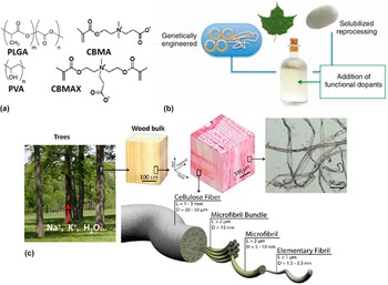
Metal foils used for interconnects were also explored for substrates, with advantages over organic polymers in low permeability of gases and liquids, absence of swelling, and direct device fabrication. Reference Kang, Hwang, Yu, Seo, Corbin, Shin, Wie, Bashir, Ma and Rogers72 But the fabrication limitation of polymer substrates was removed after transfer printing was introduced in the fabrication approach. Reference Hwang, Song, Huang, Cheng, Kang, Kim, Kim, Yu, Huang and Rogers66 To interface with biological tissues, soft and flexible polymeric materials still play dominant roles for the substrate. The synthetic materials and materials with natural origin are both important. Reference Nair and Laurencin73 A set of synthetic polymers has been developed for biodegradable substrates, Reference Hwang, Song, Huang, Cheng, Kang, Kim, Kim, Yu, Huang and Rogers66,Reference Tian, Tang, Zhuang, Chen and Jing74 including diphenylalanine (FF) and polyfluorene (PF), Reference Khanra, Cipriano, Lam, White, Fileti, Alves and Guha75 poly(vinyl alcohol) (PVA), Reference Bettinger and Bao21 polycaprolactone (PCL), Reference Tian, Tang, Zhuang, Chen and Jing74 poly lactic acid (PLA), Reference Anderson and Shive76 poly glycolic acid (PGA), Reference Middleton and Tipton77 and poly(lactic-co-glycolic acid) (PLGA) Reference Anderson and Shive76 that is a copolymer of PLA and PGA. In particular, both PVA and PLGA are inexpensive, commercially available, and widely used in biomedical devices with clinical applications [Fig. 4(a)]. Reference Tian, Tang, Zhuang, Chen and Jing74
Insulators for substrates and encapsulations. (a) Chemical structures of poly(vinyl alcohol) (PVA) and poly(L-lactide-co-glycolide) (PLGA), as well as CBMA monomer and CBMA cross-linker (CBMAX) for poly(carboxybetaine methacrylate) (PCBMA) hydrogels. Reprinted with permissions from Reference Bettinger and BaoRefs. 21 and Reference Zhang, Cao, Bai, Carr, Ella-Menye, Irvin, Ratner and Jiang80. (b) Reconstituted native silk proteins or genetically engineered silks lead to new materials and technology platforms with control of mechanical, morphological, and structural properties. Reprinted with permission from Reference Omenetto and KaplanRef. 109. (c) Three-dimensional (3D) hierarchical structure of wood fiber for metabolic ion transportation. Reprinted with permission from Reference Zhu, Jia, Chen, Weadock, Wan, Vaaland, Han, Li and HuRef. 141.

In the second category, silk consisting of two main proteins (i.e., fibroin and sericin) is one representative biopolymer, because it is biocompatible, bioresorbable, and water-soluble with programmed rates of dissolution [Fig. 4(b)]. Reference Hu, Shmelev, Sun, Gil, Park, Cebe and Kaplan78,Reference Wang, Kluge, Leisk and Kaplan79 Eliciting no immune response, silk is a widely used material for encapsulation, which will be discussed more in detail for a multilayer encapsulation strategy at the end of this subsection. Toward the same goal to overcome the foreign body responses, zwitterionic hydrogels have been developed. Reference Zhang, Cao, Bai, Carr, Ella-Menye, Irvin, Ratner and Jiang80 As a unique zwitterionic material, carboxybetaine-based poly(carboxybetaine methacrylate) (PCBMA) hydrogels prepared from a carboxybetaine monomer (CBMA) and a carboxybetaine cross-linker (CBMAX) can effectively mitigate the foreign body reaction [Fig. 4(a)]. Another protein-based polymer is gelatin, a fully biocompatible and biodegradable material that is widely used in the pharmaceutical industry for drug delivery capsules. Reference Kim, Chun, Whitacre and Bettinger81 As a low cost material, shellac has also been recently introduced as an edible coating by the food industry to preserve the freshness of fruits and vegetables during transportation. Reference Irimia-Vladu51 Another innovative report has introduced egg white, or natural chicken albumen as dielectric layer. Reference Chang, Wang, Huang, Tsai, Guo and Wen82 Made from plant-derived cellulose, paper is another prominent substrate material in the second category, Reference Hamedi, Ainla, Guder, Christodouleas, Fernandez-Abedul and Whitesides83–Reference Russo, Ahn, Adams, Duoss, Bernhard and Lewis85 with increasing attention toward paper electronics. Reference Nyholm, Nystrom, Mihranyan and Stromme86,Reference Tobjork and Osterbacka87 Though paper is inexpensive from roll-to-roll industrial manufacturing, the synthetic latex binder and natural mineral pigments such as kaolin are not fully biodegradable. Reference Irimia-Vladu51 Completely derived from wood, biodegradable cellulose nanofibril shown in Fig. 4(c) was reported as an alternative substrate for ecofriendly electronics, with a fungal degradation test to prove the concept. Reference Jung, Chang, Zhang, Yao, Zheng, Yang, Mi, Kim, Cho, Park, Jiang, Lee, Qiu, Zhou, Cai, Gong and Ma33 The transparent property of the nanopaper also makes it particularly suitable for OLED devices. Reference Zhu, Xiao, Liu, Li, Weadock, Fang, Huang and Hu88–Reference Jin, Lee, Im, Han, Jeong, Rolandi, Choi and Bae90 The cellulose-based materials are low-cost, noncytotoxic, and compatible with human blood, demonstrating great potential for biodegradable substrates, especially for scalable manufacturing to be discussed in detail in Sec. IV. B.
The stable operation of devices depends on proper passivation and encapsulation. Without proper encapsulation, certain devices would still function before conducting interconnects break, but the electrical performance changes over time. In a two-stage dissolution of dissolvable electronics, the initial period of stable operation of the device is determined by the encapsulation layer, followed by a rapid degradation determined by the dissolution of metal interconnects. MgO was explored as an encapsulation layer on top of Mg interconnects to extend the lifetime of the device. Reference Hwang, Tao, Kim, Cheng, Song, Rill, Brenckle, Panilaitis, Won, Kim, Song, Yu, Ameen, Li, Su, Yang, Kaplan, Zakin, Slepian, Huang, Omenetto and Rogers24 Without encapsulation, an Mg interconnect with an initial thickness of 300 nm functions for ∼1 h. With an MgO encapsulation layer of 400 and 800 nm, the time increases to ∼3 and ∼13 h, respectively [Fig. 3(d)].
The thickness of the encapsulation layer extends the lifetime of the device in a controlled manner, and this is further illustrated in a bilayer reactive diffusion model, where an encapsulation layer is laminated on top of the device layer. The equation of reactive diffusion still applies to each of these two layers. The concentration and flux of solution are continuous across the interface. Taken together with the updated boundary and initial conditions, the equation of reactive diffusion for the bilayer system can be analytically solved to give the concentration field of the solution as a function of time. Reference Li, Cheng, Su, Hwang, Yin, Tao, Brenckle, Kim, Omenetto, Rogers and Huang64 For the MgO/Mg system in aqueous solutions, the diffusivity of MgO encapsulation is much smaller than that of Mg, leading to a relatively uniform and low water concentration in the Mg layer in comparison to the case without MgO. In addition, the water concentration in the Mg layer increases slowly, which effectively extends the lifetime of Mg. The model also captures the effect of thickness of encapsulation layer on the dissolution of Mg, indicating thickness of encapsulation is another effective means in programming the lifetime of the device.
In silicon-based high-performance electronics, silicon oxides (SiO2) and nitrides (Si3N4) are key materials for dielectrics and encapsulations as they serve as strong barriers against water penetration.
Reference Kang, Hwang, Cheng, Yu, Kim, Kim, Huang and Rogers91
The hydrolysis of silicon oxides forms orthosilicic acid,
Reference Brady and Walther92
 ${\rm{Si}}{{\rm{O}}_2} + 2{{\rm{H}}_2}{\rm{O}} \to {\rm{Si}}{\left( {{\rm{OH}}} \right)_4}$
where the concentration of hydroxide ions has a strong effect due to their initiation of the reaction.
Reference Seidel, Csepregi, Heuberger and Baumgartel39
In aqueous solutions, silicon nitrides first oxidize to silicon oxides, followed by the hydrolysis of silicon oxides.
Reference Bergstrom and Bostedt93
The overall reaction is
 ${\rm{S}}{{\rm{i}}_3}{{\rm{N}}_4} + 12{{\rm{H}}_2}{\rm{O}} \to 3{\rm{Si}}{\left( {{\rm{OH}}} \right)_4} + 4{\rm{N}}{{\rm{H}}_3}$
. The dependence of dissolution rates on pH levels is found to be similar to that of silicon oxides, because they serve as an intermediate reaction product. Because of the ability to form a conformal coating and its established use in commercial devices, Kang et al.
Reference Kang, Hwang, Yu, Seo, Corbin, Shin, Wie, Bashir, Ma and Rogers72
also reported silicate-based spin-on glass as encapsulation and dielectric layers.
The model of reactive diffusion cannot be directly applied to understand the dissolution of silicon oxides and nitrides encapsulation layers, because the density of the layer varies in different deposition methods. For example, the densities are ∼2.3 g/cm3, ∼2.1 g/cm3, and ∼1.9 g/cm3 for thermally grown, plasma enhanced chemical vapor deposition (PECVD), and electron-beam physical vapor deposition oxides, respectively. Similarly, the density of silicon nitride is 3.1 g/cm3 for low-pressure chemical vapor deposition (LPCVD), 3.0 g/cm3 for PECVD-LF (low frequency), and 2.5 g/cm3 for PECVD-HF (high frequency). The variation in density changes the dissolution rate in two ways: (a) lower density is associated with smaller amount of materials to be dissolved for the same size of the sample; and (b) lower density corresponds to higher porosity, leading to larger effective area for reaction. To account for the effect of density in the model of reactive diffusion, effective density ρeff of the porous material should be used and it is related to the density ρs of fully dense material ρeff = ρs V s/(V s + V air), where V s and V air are the volumes of the material and air cavity in the porous structure. Following the same procedure, the model of reactive diffusion can be solved to give the remaining thickness of the porous material, which reproduced the experimental measurements of silicon oxides and nitrides. The reaction constants are found to be slightly different for the dissolution of silicon oxides and nitrides from various methods of deposition, which may be attributed to bond strength. Reference Kang, Hwang, Cheng, Yu, Kim, Kim, Huang and Rogers91 Future work on the dissolution at atomic scale is needed to uncover the underlying mechanism.
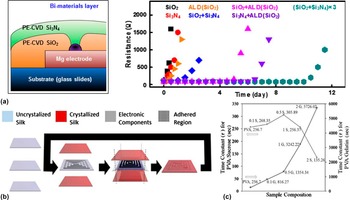
The thickness of encapsulation provides an effective means to extend the lifetime of the device, but it is not practical when the period of stable operation spans days or even weeks. An encapsulation layer with low water diffusivity such as one made of a silicon oxide or a nitrite is desirable, as it can serve as a barrier layer to slow down water penetration. However, the pinholes and the other defects in the encapsulation provide water leakage pathways, leading to the breakdown of the device. Therefore, the design of a multilayer structure with different materials offers a unique solution to cooperatively eliminate the defect density and significantly increase the lifetime of the device. As shown in Fig. 5(a), an Mg trace of 300 nm with several encapsulation layouts was studied. As an alternative to the deposition methods discussed above, atomic layer deposition (ALD) with few defects is effective to reduce the defect density. Reference Dameron, Davidson, Burton, Carcia, McLean and George94 In comparison to the increase of a few hours for the Mg trace with a single encapsulation of ALD SiO2 (20 nm) or PECVD SiO2 (Si3N4) (1 μm), a bilayer of PECVD SiO2 and Si3N4 (500 nm each) can extend the time to ∼1 day. Another bilayer of PECVD SiO2 (or Si3N4, 500 nm) and ALD SiO2 (20 nm) further increases this time to 5 days (or 7 days). In addition, a triple layer of alternating PECVD SiO2 and Si3N4 (200/200/200/200/100/100 nm, total thickness of 1 μm) extends the time to ∼10 days, illustrating the cooperative elimination of defect pathways. The multilayer structure was also demonstrated in systems with the other encapsulation materials. As an example, silk overcoat was applied on top of MgO encapsulation for Mg interconnects to extend the lifetime by a few factors in Fig. 3(d). Silk overcoat is of particular interest, because of its tunable crystalline and diffusion properties. With minimal immunogenicity, silk can also be applied in the form of pocket to improve the in vivo behavior of the device. Direct application of silk pocket presents challenge, however, because sagging of silk introduces mechanical stress to the devices and exposes them directly to water. To address this issue, Brenckle et al. Reference Brenckle, Cheng, Hwang, Tao, Paquette, Kaplan, Rogers, Huang and Omenetto95 introduced encapsulation of multiple air pockets fabricated from silk fibroin, with a scheme demonstrated in Fig. 5(b). Sealing of the silk encapsulation and substrate enclosed the device in an air pocket and iteration of this process created multiple air pockets as needed. Onset degradation of the device started when the swelling of silk clasped the multiple air pockets. In another example, Acar et al. Reference Acar, Çınar, Thunga, Kessler, Hashemi and Montazami96 explored a composite insulating structure with addition of gelatin or sucrose to a PVA polymer matrix to either slow or enhance the transiency of the composite. The dissolution curves as a function of time were fitted with inversed exponential functions. The lower time constants in the inversed exponential function correspond to faster transiency. As shown in Fig. 5(c), an increase in the ratio of gelatin slows down the transiency of the composite, thereby extending the lifetime of the device.
Multilayer encapsulation strategy. (a) (Left) Combination of different material layers (Si3N4 and SiO2) for transient electronics encapsulation. Defect such as the pinhole shown in the figure is covered by the bilayer structure. (Right) Electrical resistance of Mg traces (300 nm) encapsulated by different materials and thicknesses is measured after immersion in DI water at room temperature for different periods of time. Black: 1 μm PECVD SiO2 single layer; Red: 1 μm PECVD-LF Si3N4 single layer; Orange: 20 nm ALD SiO2 single layer; Blue: 500 nm PECVD SiO2/500 nm PECVD-LF Si3N4 bilayer; Magenta: 500 nm PECVD SiO2/20 nm ALD SiO2 bilayer; Purple: 500 nm PECVD-LF Si3N4/20 nm ALD SiO2 bilayer; Cyan: alternately laminated PECVD SiO2 and PECVD-LF Si3N4 layers (200/200/200/200/100/100 nm). Reprinted with permission from Reference Kang, Hwang, Cheng, Yu, Kim, Kim, Huang and RogersRef. 91. (b) Fabrication process of the silk pocket that utilizes three silk films for each pocket. Inner silk film remains uncrystallized and serves as substrate while outer layers are crystallized to be water insoluble depending on the required degradation characteristics. Sealing of the edges of outer films encapsulates the device and repeating this process creates multiple silk pockets. Reprinted with permission from Reference Brenckle, Cheng, Hwang, Tao, Paquette, Kaplan, Rogers, Huang and OmenettoRef. 95. (c) Time constant for composites with different ratios of sucrose and gelatin. 0.1 G/S, 0.5 G/S, 1 G/S, and 2 G/S correspond to weight ratio of PVA to gelatin/sucrose of 10:1, 2:1, 1:1, and 1:2, respectively. Reprinted with permission from Reference Acar, Çınar, Thunga, Kessler, Hashemi and MontazamiRef. 96.

III. FUNCTIONAL DISSOLVABLE DEVICES
Demonstrated applications of inorganic dissolvable electronics range from simple active components such as Si diodes, Reference Hwang, Tao, Kim, Cheng, Song, Rill, Brenckle, Panilaitis, Won, Kim, Song, Yu, Ameen, Li, Su, Yang, Kaplan, Zakin, Slepian, Huang, Omenetto and Rogers24,Reference Hwang, Huang, Seo, Song, Kim, Hage-Ali, Chung, Tao, Omenetto, Ma and Rogers97 inverters, Reference Hwang, Song, Huang, Cheng, Kang, Kim, Kim, Yu, Huang and Rogers66,Reference Hwang, Huang, Seo, Song, Kim, Hage-Ali, Chung, Tao, Omenetto, Ma and Rogers97,Reference Hwang, Kim, Tao, Kim, Kim, Yu, Panilaitis, Jeong, Song and Omenetto98 and n- and p-channel transistors, Reference Hwang, Tao, Kim, Cheng, Song, Rill, Brenckle, Panilaitis, Won, Kim, Song, Yu, Ameen, Li, Su, Yang, Kaplan, Zakin, Slepian, Huang, Omenetto and Rogers24,Reference Hwang, Song, Huang, Cheng, Kang, Kim, Kim, Yu, Huang and Rogers66,Reference Hwang, Huang, Seo, Song, Kim, Hage-Ali, Chung, Tao, Omenetto, Ma and Rogers97,Reference Jin, Shin, Cho, Han, Lee, Lee, Lee and Rogers99 to integrated systems that include hydration sensors, Reference Hwang, Song, Huang, Cheng, Kang, Kim, Kim, Yu, Huang and Rogers66 pH sensors, Reference Hwang, Lee, Cheng, Jeong, Kang, Kim, Shin, Yang, Liu, Ameer, Huang and Rogers100 strain and temperature sensors, Reference Hwang, Tao, Kim, Cheng, Song, Rill, Brenckle, Panilaitis, Won, Kim, Song, Yu, Ameen, Li, Su, Yang, Kaplan, Zakin, Slepian, Huang, Omenetto and Rogers24 electrophysiological sensors, Reference Hwang, Lee, Cheng, Jeong, Kang, Kim, Shin, Yang, Liu, Ameer, Huang and Rogers100 thin-film solar cells, Reference Hwang, Tao, Kim, Cheng, Song, Rill, Brenckle, Panilaitis, Won, Kim, Song, Yu, Ameen, Li, Su, Yang, Kaplan, Zakin, Slepian, Huang, Omenetto and Rogers24,Reference Kang, Park, Kim, Hwang, Cheng, Shin, Chung, Kim, Yin, Lee, Lee and Rogers44 array of photodetectors, Reference Hwang, Tao, Kim, Cheng, Song, Rill, Brenckle, Panilaitis, Won, Kim, Song, Yu, Ameen, Li, Su, Yang, Kaplan, Zakin, Slepian, Huang, Omenetto and Rogers24 mechanical energy harvesters, Reference Dagdeviren, Hwang, Su, Kim, Cheng, Gur, Haney, Omenetto, Huang and Rogers49 RF power scavengers, Reference Hwang, Huang, Seo, Song, Kim, Hage-Ali, Chung, Tao, Omenetto, Ma and Rogers97 batteries, Reference Yin, Huang, Xu, Zhang, Lam, Cheng and Rogers101,Reference Tsang, Armutlulu, Herrault, Shafer, Allen and Allen102 and pressure sensor array for cardiovascular monitoring. Reference Boutry, Nguyen, Lawal, Chortos, Rondeau-Gagne and Bao103 The initial conceived application in biomedical implants is of particular interest, but the capabilities to transform the function and dissolve on demand also open up new opportunities for dissolvable devices.
A. Dissolvable batteries
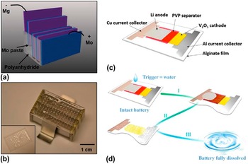
As in conventional devices, power supply is a crucial component in dissolvable electronics. Demonstrated strategies include near-field radio frequency power transfer modules, Reference Hwang, Huang, Seo, Song, Kim, Hage-Ali, Chung, Tao, Omenetto, Ma and Rogers97 mechanical energy harvesters, Reference Dagdeviren, Hwang, Su, Kim, Cheng, Gur, Haney, Omenetto, Huang and Rogers49 and silicon based solar cells, Reference Hwang, Tao, Kim, Cheng, Song, Rill, Brenckle, Panilaitis, Won, Kim, Song, Yu, Ameen, Li, Su, Yang, Kaplan, Zakin, Slepian, Huang, Omenetto and Rogers24 though each has significant shortcomings. In addition to water-activated edible batteries Reference Kim, Chun, Whitacre and Bettinger81,Reference Sammoura, Lee and Lin104 that have partial constituent materials to be transient, fully biodegradable primary batteries have also been introduced. Reference Yin, Huang, Xu, Zhang, Lam, Cheng and Rogers101 The demonstrated device used dissolvable metals for the electrodes and biodegradable polymers for barrier layers and encapsulations. Though metallic cathodes reduce the operating voltage and output current density, it is possible to compensate by series connecting batteries to increase the voltage and enlarging the battery area for higher current density. As shown in Fig. 6(a), four Mg–Mo cells separated by polyanhydride layers are connected in series by a Mo paste buried in the polyanhydride encasement. In addition, thin polyanhydride film with porous structures serves as a top cover to retain the electrolyte due to positive contact angle, while permitting the release of hydrogen gas [Fig. 6(b)]. The polyanhydride encasement in the battery dissolves first, leaving partially dissolved Mg and Mo to slowly degrade after 11 days in PBS at body temperature.
Transient batteries. (a) A battery pack consists of four Mg-Mo cells in series separated by polyanhydride spacers. (b) Optical image of the battery shows porous polyanhydride (inset) as a top cover to confine electrolytes. (a)–(b): reprinted with permission from Reference Yin, Huang, Xu, Zhang, Lam, Cheng and RogersRef. 101. (c) Schematic illustration of the transient rechargeable battery. (d) When triggered by water, cascade reactions lead to a complete dissolution of every battery component. (c)–(d): reprinted with permission from Reference Fu, Liu, Yao, Wang, Zhao, Luo, Dai, Lacey, Zhou, Shen, Kim, Swafford, Sengupta and HuRef. 118.

Rechargeable modules in battery Reference Xu, Zhang, Cho, Lee, Huang, Jia, Fan, Su, Su, Zhang, Cheng, Lu, Yu, Chuang, Kim, Song, Shigeta, Kang, Dagdeviren, Petrov, Braun, Huang, Paik and Rogers105 offer unique opportunities for repeated use. Combining with the idea of transient technology, Fu et al. Reference Yin, Huang, Xu, Zhang, Lam, Cheng and Rogers101 reported the first transient rechargeable battery based on lithium ion batteries Reference Fu, Wang, Yan, Liu, Yao, Dai, Hitz, Wang, Luo and Chen106 [Fig. 6(c)]. This battery exploited vanadium oxide (V2O5) for the cathode, due to its high capacity and ability to dissolve in alkali solutions formed when lithium (Li) metal anode reacted with water. To achieve fast dissolution for the entire battery system, water-soluble polyvinylpyrrolidone (PVP) and sodium alginate (Na-AG) were selected for separators and battery encasements, respectively. The battery (0.5 cm by 1.0 cm; total mass of 0.1 g; energy of 0.1 J) was fabricated by a combination of cut-and-stack and shadow mask metal depositions. When triggered by water, cascade reactions started from the dissolution of Li anode, followed by a complete disappearance of all components in the alkali solution to the naked eye within minutes [Fig. 6(d)]. In addition to high voltage and capacity, the battery with property size and mass demonstrated stable discharge–charge curves. Although the flexible design of this rechargeable transient battery can meet various voltage and capacity requirements, the alkaline solution generated from the cascade reaction is not compatible with human body. For potential applications in environmental sensors, their impact on the environment also needs to be closely examined, whereas this characteristic is not critical in security or military related applications. Therefore, rechargeable transient battery with biologically and environmentally benign end products remains a direction for the future development. It is also desirable to develop miniaturized cells with small footprint/size for implantable applications, as well as wireless power transfer to deep-tissue implants. Reference Ho, Yeh, Neofytou, Kim, Tanabe, Patlolla, Beygui and Poon107 With functional power supply modules specifically designed for each application, dissolvable electronics are on their way in finding new opportunities.
B. Biomedical implants
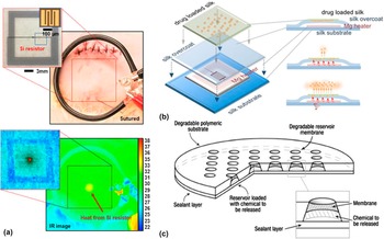
Implantable devices are direct applications of dissolvable electronics in biomedicine. Hwang et al. Reference Hwang, Tao, Kim, Cheng, Song, Rill, Brenckle, Panilaitis, Won, Kim, Song, Yu, Ameen, Li, Su, Yang, Kaplan, Zakin, Slepian, Huang, Omenetto and Rogers24 first demonstrated an inorganic thermal therapy device through a series of in vitro and in vivo experiments. Placed below an agar plate of 3 mm loaded with Escherichia coli bacteria, a metamaterial radio frequency (RF) antenna included one Mg RF inductive coil to transmit power and one Mg resistor to serve as a heater. The center of the plate that corresponds to the heater position was heated to ∼50 °C, whereas the control samples (with only an Mg resistor or an Mg inductor) showed negligible heating. The local absence zone of bacteria was clearly observed in the heated region and there was no noticeable change for the controls, after 30 min heating followed by lawn growth in a 37 °C incubator overnight. In addition, bacterial inhibition could be enhanced by both power (thus temperature) and duration. Reference Tao, Hwang, Marelli, An, Moreau, Yang, Brenckle, Kim, Kaplan, Rogers and Omenetto108 To demonstrate the biodegradation of the device in vivo, a thermal therapy device was implanted under the skin of a female albino Sprague–Dawley rat [Fig. 7(a), top]. In the device, a doped Si nanomembrane serving as a resistor was connected to a wireless Mg inductor by an Mg interconnect. Transfer of the Si resistor on an untreated silk film was followed by subsequent deposition and patterning of Mg inductor, MgO interlayer, and Mg interconnect. Encapsulating in a silk package then completed the fabrication process. When powered by a near-field inductive coupling through the skin, the device generated a localized temperature increase (ΔT ∼5 °C) corresponding to the location of the heater [Fig. 7(a), bottom]. Designed by the property of the silk pocket, the operation time of the device was chosen to be 15 days to coincide with the medically critical timeframe for maintaining asepsis at the wound site.
Biomedical implants with in vitro and in vivo demonstrations. (a) Primary coil on top of the sutured implant site, with a thermal therapy device shown in the inset (Top). Temperature rise of 5 °C (magnified view in the inset) between the heating zone and background is observed during powering of the device (Bottom). Adapted with permission from Reference Hwang, Tao, Kim, Cheng, Song, Rill, Brenckle, Panilaitis, Won, Kim, Song, Yu, Ameen, Li, Su, Yang, Kaplan, Zakin, Slepian, Huang, Omenetto and RogersRef. 24. (b) Schematic illustration of the wirelessly activated drug release device with loaded drug in the silk film (Orange dots: ampicillin molecules; Green matrix: silk film). Wirelessly activated heater increases the temperature and promotes the antibiotic release. Reprinted with permission from Reference Tao, Hwang, Marelli, An, Moreau, Yang, Brenckle, Kim, Kaplan, Rogers and OmenettoRef. 108. (c) Schematic of polymeric microchip device for multi-pulse drug delivery. Degradable polymer substrate with patterned reservoirs for drug loading is sealed with degradable reservoir membranes on one side and a polyester sealant tape on the other side. A magnified view of a reservoir shows the reservoir membrane, polyester tape, and loaded chemical. Reprinted with permission from Reference Grayson, Choi, Tyler, Wang, Brem, Cima and LangerRef. 110.

Silk used in the aforementioned study not only is a suitable biomaterial for substrate and encapsulation, but also has the potential for wirelessly controlled drug stabilization and release because of its ability to load stable therapeutic compounds. Reference Omenetto and Kaplan109 As shown in Fig. 7(b), Tao et al. Reference Tao, Hwang, Marelli, An, Moreau, Yang, Brenckle, Kim, Kaplan, Rogers and Omenetto108 tested this paradigm in a series of in vitro experiments. Ampicillin solution was first mixed with 6 wt% silk solution to load the antibiotic in the silk film, and then integrated on top of a wireless Mg heater encapsulated by a silk pocket. Wireless activation triggered the continuous release of the drug. Both silk solution extraction time and water-vapor annealing were shown to affect the antibiotic release kinetics. Reference Tao, Hwang, Marelli, An, Moreau, Yang, Brenckle, Kim, Kaplan, Rogers and Omenetto108 The increase in temperature also enhanced the drug release due to increased diffusivity of the antibiotic and temperature-driven annealing of wet silk chains. In addition to loading the drug to biomaterials for continuous release, biodegradable materials can also serve as reservoirs for pulsatile release. As shown in Fig. 7(c), truncated conical reservoirs in the biodegradable polymeric substrate were loaded with chemicals, and sealed with biodegradable membranes of different dissolution time. Reference Grayson, Choi, Tyler, Wang, Brem, Cima and Langer110 Multi-pulses of drug were released when each membrane was sequentially degraded and opened. The timing of each release was controlled by the design of each membrane, thereby eliminating the need for external stimuli to trigger the drug release over the period of months. Although this strategy works well for pulsatile release at designed time, it cannot meet the need to release drug on-demand. A combination of these two strategies will create opportunities for future drug delivery systems.
C. Function transformation
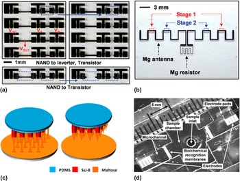
The capability to program function transformation of the device provides versatility in the design and opens additional opportunities for dissolvable electronics. A simple strategy is to utilize variations in types and thicknesses of materials to dissolve different components in a programmed manner. In Fig. 8(a), a patterned encapsulation layer of MgO allows a rapid dissolution of Mg in the locations without MgO encapsulation, leading to functional transformation in NAND gates. Reference Hwang, Kang, Huang, Brenckle, Omenetto and Rogers111 The first and second rows in Fig. 8(a) correspond to the transformation of NAND gates to inverters and individual n-channel MOSFETs, respectively. In addition, transformation of function can result from a switch between two components connected in parallel (e.g., a resistor and a diode). At low electrical bias, most of the current flows through the resistor due to low resistance. When the encapsulation is only applied to the diode, the resistor without encapsulation dissolves and leaves the circuit with only the diode. The same concept can be applied to the other circuit designs as well.
Functional transformation of the device by dissolving its key components. (a) Transformation from a NAND gate (left) to an inverter and transistor (right) is accomplished by dissolution of the Mg interconnect. (b) A transient Mg antenna connected to an Mg resistor (thickness, 2.5 μm), encapsulated by SiO2 of 2 μm and MgO of 800 nm except the regions indicated in the figure by blue and red boxes. (a)–(b): reprinted with permission from Reference Hwang, Kang, Huang, Brenckle, Omenetto and RogersRef. 111. (c) After immersing the SU-8 microtubes in the liquid maltose at 140 °C followed by a gradual temperature increase to 160 °C, SU-8 microtubes are drawn away from the interface. Shrinking and breaking of individual maltose bridge creates a sharp tip on top of each SU-8 microtube. Reprinted with permission from Reference Xiang, Wang, Pant, Pastorin and LeeRef. 113. (d) Autonomous microfluidic sensing device that transduces chemical and biological signal to a large output voltage, when the target fluid dissolves biological/chemical recognition membranes and connects the electrodes. Reprinted with permission from Reference Sridharamurthy, Agarwal, Beebe and JiangRef. 114.

Transformation of geometry from dissolution provides another means to tune circuit characteristics. As an example shown in Fig. 8(b), Hwang et al. Reference Hwang, Kang, Huang, Brenckle, Omenetto and Rogers111 demonstrated radio frequency (RF) antennas with tunable shifts in the resonance frequency. Connected to an Mg resistor, an Mg antenna was encapsulated at selected regions with thin and less effective layers (400 and 800 nm MgO in stages 1 and 2), in comparison to the effective encapsulation in the other regions (MgO of 800 nm and SiO2 of 2 μm). The dissolution started at the location with thin encapsulation, leading to the progressively shortened length of the antenna and thus higher resonance frequency. Via a similar idea, resonance frequency of an Mg inductor can be changed through dissolution of local interconnects. Elimination of crossing between adjacent lines altered the current flow generated from inductive coupling, contributing to the decrease of the resonance frequency. The design on variation of encapsulation thickness can also be realized by replacing encapsulated regions 1 and 2 with two different materials, so that corresponding etchant can initiate the transformation in a sequential and selective manner. Reference Lee, Kang, Salvatore, Ma, Kim, Jiang, Kim, Yan, Wie, Banks, Oh, Feng, Huang, Troester and Rogers112 Other applications include reconfigurable circuits for signal processing. For example, gain of analog amplifiers and oscillation frequency of square waveform generators can be tuned by the selective dissolution of resistors/interconnects.
Coupling the above ideas with the other functional components provided additional control in functional transformation through the control of dissolution. Figure 8(c) presents an innovative process to fabricate microneedle array for transdermal drug delivery. Reference Xiang, Wang, Pant, Pastorin and Lee113 In comparison to the traditional time-consuming fabrication approach that deploys various molds to create sharp tips at the end of needles for penetration, drawing SU-8 microtubes immersed in the maltose at an increased speed form sharp tips at the end of microtubes. After penetrating the skin's outer barrier layer (stratum corneum), all of the maltose tips are easily dissolved in the tissue, allowing continuous delivery of the drug via biocompatible microtubes.
In another example shown in Fig. 8(d), dissolvable membrane can also be used as a sensing element in simple microfluidic devices to transduce chemical and biological signals into electrical signals with large amplification. Reference Sridharamurthy, Agarwal, Beebe and Jiang114 Electrodes separated by biological/chemical recognition membranes are initially in the air with large resistance. These membranes become porous and eventually dissolve in the fluid, with dissolution time characteristic determined by the concentration of fluid. The movement of fluid connects the two electrodes, which dramatically changes the resistance. By defining the membrane specific to the target, a range of targets such as toxins can be detected. The design concept can also be applied to other microfluidic systems. For example, dissolvable bridges Reference Houghtaling, Liang, Thiessen and Fu115 or valves Reference Gorkin, Nwankire, Gaughran, Zhang, Donohoe, Rook, O'Kennedy and Ducrée116 can be used to control the close or open of the flow of fluids. As discussed in the previous subsection, it is also useful to program functional transformation upon user-defined signals and this type of triggered transience will be introduced more in detail in the next subsection.
D. Triggered transience
The lifetime of the device is defined by the encapsulation layer and therefore, it is controlled by the encapsulation strategy selected at the initial fabrication. Significant utility of dissolvable devices is evident if active control of their lifetime can be achieved. Metastable polymers can depolymerize rapidly by specific stimuli, thereby providing a unique means to precisely control the lifetime of the device. To respond to a specific trigger (e.g., chemical, Reference Seo and Phillips117 humidity, Reference Fu, Liu, Yao, Wang, Zhao, Luo, Dai, Lacey, Zhou, Shen, Kim, Swafford, Sengupta and Hu118 temperature, Reference Park, Kang, Hernandez, Kaitz, Wie, Shin, Lee, Sottos, Moore, Rogers and White119 or light Reference Hernandez, Kang, Lee, Hwang, Kaitz, Inci, Park, Chung, Sottos, Moore, Rogers and White120 ), the metastable polymers must possess the following two properties: (a) robust performance as a substrate or encapsulant with tunable degradation kinetics, and (b) triggered depolymerization to deactivate the device.
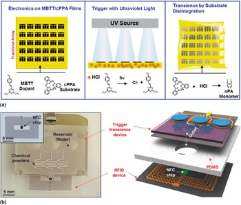
To demonstrate a phototriggerable dissolvable device, Hernandez et al. Reference Hernandez, Kang, Lee, Hwang, Kaitz, Inci, Park, Chung, Sottos, Moore, Rogers and White120 explored arrays of transistors and diodes on a cyclic poly(phthalaldehyde) (cPPA) substrate with a photo-acid generator (PAG) 2-(4-methoxystyryl)- 4,6-bis(trichloromethyl)-1,3,5-triazine (MBTT) additive. The films maintained robust mechanical properties in ambient conditions until they were exposed to ultraviolet (UV) lights. The irradiance of the UV source generated HCl from MBTT and triggered the dissolution of the PAG/cPPA substrate, leading to deactivation of the electronics [Fig. 9(a)]. Similar to the idea of light trigger, Park et al. Reference Park, Kang, Hernandez, Kaitz, Wie, Shin, Lee, Sottos, Moore, Rogers and White119 also demonstrated a heat trigger to deactivate the device. In addition to fast device destruction, heat triggers can also be coupled with light, magnetic, or RF through photothermal nanomaterials or induction heating Reference Hwang, Tao, Kim, Cheng, Song, Rill, Brenckle, Panilaitis, Won, Kim, Song, Yu, Ameen, Li, Su, Yang, Kaplan, Zakin, Slepian, Huang, Omenetto and Rogers24,Reference von Maltzahn, Park, Agrawal, Bandaru, Das, Sailor and Bhatia121,Reference Hoare, Santamaria, Goya, Irusta, Lin, Lau, Padera, Langer and Kohane122 to provide other triggering modalities.
The idea to destroy electronics on demand also finds applications in data security. Though vulnerable, data encryption and access passwords are still widely used approaches to effectively protect confidential data. As opposed to software approaches, destruction of the hardware presents ultimate solution to secure data. To demonstrate the idea, wireless microfluidic components were explored to permanently remove the key constituent materials in integrated circuits. Reference Lee, Jeong, Liu, Zhang, Shi, Kang, Kim, Kim, Lee, Kim, Jang, Yin, Kim, Banks, Paik, Huang and Rogers35 As shown in Fig. 9(b), a wireless microfluidic device consisted of (a) micro-fabricated thermal actuators, (b) thermally expandable polymers, (c) fluid reservoirs, and (d) microfluidic channels with embedded enchant powders. Each thermal actuator can be controlled independently to induce Joule heating, resulting in an increase in volume of thermally expandable polymer when heated above 80 °C. The drastic volume change nearly fills the reservoir regions, and ejection of water from the reservoirs mix with powders embedded in the serpentine microfluidic channels to form etchants. The resulting etchants directed by the outlet can selectively remove the target components and lead to functional degradation of the device. In the example shown in Fig. 9(b), an unpackaged near field communication (NFC) chip was connected to a Cu inductive coil by an In/Ag solder paste to form a radio frequency identification device (RFID). Reference Kim, Banks, Cheng, Xie, Xu, Jang, Lee, Liu, Gutruf, Huang, Wei, Liu, Li, Dalal, Ghaffari, Feng, Huang, Gupta, Paik and Rogers123 The triggered release of KHF etchant destroyed the NFC chip as well as the interconnections between the chip and Cu coil. The abrupt functional degradation stopped the power/data communication of the NFC chip within 3 s. However, the liquids can only be retained in the microfluidic system for a relatively short time (∼1 week) and advancement in conventional microfluidics is expected to extend this time.
Dissolution on demand. (a) The destruction of electronics integrated on MBTT/cPPA substrate (left) is triggered by exposing the substrate to ultraviolet light, which generates HCl (middle) that rapidly depolymerizes cPPA and dissolves the Mg electrodes (right). Reprinted with permission from Reference Hernandez, Kang, Lee, Hwang, Kaitz, Inci, Park, Chung, Sottos, Moore, Rogers and WhiteRef. 120. (b) Optical image (left) and schematic illustration (right) of wirelessly triggered dissolvable radio frequency identification device (RFID) device. A microfluidic system integrated with the RFID device enables the trigger by directing the etchant to the NFC chip (shown in the inset) through the predefined holes in PDMS substrate. Reprinted with permission from Reference Lee, Jeong, Liu, Zhang, Shi, Kang, Kim, Kim, Lee, Kim, Jang, Yin, Kim, Banks, Paik, Huang and RogersRef. 35.

IV. PERSPECTIVES AND CONCLUSIONS
Although dissolvable devices have addressed many of the unmet needs in biomedical applications, there still remain opportunities for the future developments. Dissolvable devices with stretchable mechanics and scalable manufacturing characteristics represent two possible directions. The early explorations for these two directions are discussed in the following.
A. Biodegradable, stretchable devices
Application of dissolvable electronics for implantable devices ultimately hinges on the development of stretchable characteristics to conform electronics onto the complex topology of various tissues. A combined strategy in materials and mechanics opens opportunities for devices that can deform to arbitrary surfaces. Reference Rogers, Someya and Huang124,Reference Kim, Lu, Ma, Kim, Kim, Wang, Wu, Won, Tao, Islam, Yu, Kim, Chowdhury, Ying, Xu, Li, Chung, Keum, McCormick, Liu, Zhang, Omenetto, Huang, Coleman and Rogers125 The core idea is to assemble rigid device components connected by serpentine interconnects on a stretchable polymeric substrate. Reference Zhang, Fu, Su, Xu, Cheng, Fan, Hwang, Rogers and Huang126–Reference Kim, Bae, Kim, Cheng, Kim, Kim, Li, Wu, Du, Kim, Kim, Estrada, Hong, Huang, Pop and Rogers128 Interconnects deform out-of-plane to accommodate the large deformation and this leaves minimal deformation in the rigid device components that are strongly bonded to the substrate. To exploit this idea for stretchable configuration in dissolvable electronics, a dissolvable substrate with stretchable property is required. To this end, Hwang et al. Reference Hwang, Lee, Cheng, Jeong, Kang, Kim, Shin, Yang, Liu, Ameer, Huang and Rogers100 studied stretchable configuration of the device on poly(1,8-octanediol-co-citrate (POC), Reference Yang, Webb and Ameer129 a stretchable elastomer with controllable mechanical and biodegradation properties. The deformation behavior of device components connected by metal interconnects was captured by the finite element simulation. The simulation results indicated a large stretchability (>40 %) for the system with bonded device components (to the substrate) and nonbonded interconnects. However, the stretchability of the system was significantly reduced when an encapsulation layer was applied, as the encapsulation restricted the out-of-plane motion of the freestanding interconnects. Therefore, it is desirable to construct device components on raised substrate islands such that interconnects can deform into the free space in the structured substrate. Reference Lee, Wu, Shi, Yoon, Park, Li, Liu, Huang and Rogers130,Reference Liu, Cheng and Wu131
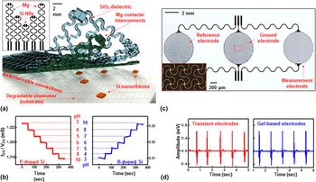
The stretchable mechanics is of particular interest to biomedical applications that require conformal contact on a time-dynamic, curvilinear surface. A stretchable pH monitor demonstrated utility in this area [Fig. 10(a)]. The fabrication of the device started with transfer of doped Si nanoribbons on a Si wafer coated with a bilayer of PMMA/D-PI. Depositions of Mg contacts/interconnects from E-beam and SiO2 dielectric from PECVD were followed by a patterned etching through a second D-PI mask. Immersing in acetone removed the sacrificial PMMA layer, enabling retrieval of the device onto a PDMS stamp. After removing the bottom D-PI layer in RIE, the device was transfer printed on a POC substrate. Etching the top D-PI layer and functionalizing Si nanoribbons with 3-aminopropyltriethoxysilane (APTES) yielded the completed system. In the pH sensor, the –NH2 and –SiOH groups on the functionalized surface protonated to –NH3 + at low pH levels and deprotonated to –SiO− at high pH levels. The conductance of phosphorus- and boron-doped Si underwent a step decrease or increase as the pH level increased from 3 to 10 [Fig. 10(b)].
The design concept on stretchable configurations can also be applied to stretchable, transient electrophysiological sensors for vital signal measurements, including electroencephalogram (EEG), Reference Kim, Lu, Ma, Kim, Kim, Wang, Wu, Won, Tao, Islam, Yu, Kim, Chowdhury, Ying, Xu, Li, Chung, Keum, McCormick, Liu, Zhang, Omenetto, Huang, Coleman and Rogers125,Reference Norton, Lee, Lee, Lee, Kwon, Won, Jung, Cheng, Jeong and Akce132 electrocardiogram (ECG), Reference Xu, Gutbrod, Bonifas, Su, Sulkin, Lu, Chung, Jang, Liu, Ying, Lu, Webb, Kim, Laughner, Cheng, Liu, Ameen, Jeong, Kim, Huang, Efimov and Rogers71,Reference Kim, Lu, Ma, Kim, Kim, Wang, Wu, Won, Tao, Islam, Yu, Kim, Chowdhury, Ying, Xu, Li, Chung, Keum, McCormick, Liu, Zhang, Omenetto, Huang, Coleman and Rogers125,Reference Jeong, Kim, Cheng, Yeo, Huang, Liu, Zhang, Huang and Rogers133 electromyography (EMG), Reference Kim, Lu, Ma, Kim, Kim, Wang, Wu, Won, Tao, Islam, Yu, Kim, Chowdhury, Ying, Xu, Li, Chung, Keum, McCormick, Liu, Zhang, Omenetto, Huang, Coleman and Rogers125,Reference Jeong, Yeo, Akhtar, Norton, Kwack, Li, Jung, Su, Lee, Xia, Cheng, Huang, Choi, Bretl and Rogers134,Reference Jang, Han, Xu, Mathewson, Zhang, Jeong, Kim, Webb, Lee, Dawidczyk, Kim, Song, Yeo, Kim, Cheng, Rhee, Chung, Kim, Chung, Lee, Yang, Cho, Gaspar, Carbonari, Fabiani, Gratton, Huang and Rogers135 and electrooculography (EOG). Reference Jang, Han, Xu, Mathewson, Zhang, Jeong, Kim, Webb, Lee, Dawidczyk, Kim, Song, Yeo, Kim, Cheng, Rhee, Chung, Kim, Chung, Lee, Yang, Cho, Gaspar, Carbonari, Fabiani, Gratton, Huang and Rogers135 As shown in Fig. 10(c), Mg trace of 300 nm coated with SiO2 dielectrics of 100 nm formed in serpentine shapes for measurement, ground, and reference electrodes, as well as connecting leads between electrodes and a data acquisition system. In comparison to conventional gel electrodes, high fidelity capacitive sensing was achieved when the Mg electrodes coupled to the skin through a thin sheet of POC layer [Fig. 10(d)].
B. Scalable manufacturing
Scalable manufacturing represents another direction for the future development of dissolvable electronics. The development in this area promises wide adoption of dissolvable consumer electronics to minimize the electronic wastes generated from obsolescence due to the rapid decrease in the lifetime of the electronics. Reference Jung, Chang, Zhang, Yao, Zheng, Yang, Mi, Kim, Cho, Park, Jiang, Lee, Qiu, Zhou, Cai, Gong and Ma33 To provide mechanical support and electrical connections for the mounted components, printed circuit boards (PCBs) are indispensable in nearly all forms of commercial devices. With multilayer configurations, PCBs provide robust and reliable performance with minimal transmission loss over extended periods of time.
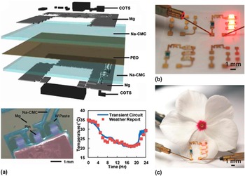
As a starting point to provide a complete picture for large scale manufacturing of dissolvable devices, Huang et al. Reference Huang, Liu, Hwang, Kang, Patnaik, Cortes and Rogers136 developed dissolvable PCBs with dissolvable metal traces and dielectric interlayers on a flexible substrate. As shown in Fig. 11(a), a thin layer of poly(ethylene oxide) (PEO, 1 μm) was sandwiched between two sodium carboxymethylcellulose (Na-CMC, 50 μm) substrates, with dissolvable metal pastes filling via holes for electrical connection between the top and bottom circuits. Commercial-off-the-shelf (COTS) components were also mounted on PCBs by using these dissolvable metal pastes as adhesive to connect the pins of COTS components to the contact pads on PCBs [Fig. 11(a), bottom left]. A transmission antenna generated 3 V in the wireless power harvester for device operation. The measurements of ambient temperature were communicated wirelessly to an external recording system, and the recordings compared favorably to those from local weather report [Fig. 11(a), bottom right]. Screen printing i.e., widely used in conventional device manufacturing also finds application in fabricating dissolvable electronics. Dissolvable metal pastes that were screen printed on Na-CMC substrates yielded antennas for wireless power transmission and coils in RFID for near field communication. When connected to an LED, the antenna provided a power output of 20 W at 1.03 GHz at an operating distance of 1 m. For a coil of 40 mm by 40 mm, when connected to a capacitor of 130 pF and an NFC chip with a capacitance of 17 pF, its intrinsic resonance frequency of 109 MHz changed to 13.5 MHz, demonstrating utility in data and power transmissions.
Dissolvable devices with stretchable mechanics. (a) Schematic illustration of biodegradable, stretchable pH sensors based on doped Si nanoribbons with a top view in the inset. (b) Conductance of the devices when immersed in solutions of different pH levels (from 3 to 10) for phosphorus (left) and boron (right) doped Si nanoribbons. (c) Optical image of a capacitive biodegradable, stretchable electrophysiological (EP) sensor. The inset shows a magnified view of the filamentary serpentine mesh electrodes. (d) EMG signal collected by biodegradable, stretchable EP sensor (left) and standard gel-based electrode (right). (a)–(d): reprinted with permission from Reference Hwang, Lee, Cheng, Jeong, Kang, Kim, Shin, Yang, Liu, Ameer, Huang and RogersRef. 100.

Scalable manufacturing via an early demonstration. (a) Exploded view schematic illustration of a representative dissolvable printed circuit board (PCB) device (top) used to sense ambient temperature and wirelessly transmit data. It consists of water dissoluble polymer films, dissolvable metal patterns, and commercial off-the-shelf (COTS) components. SEM image of a COTS component mounted by W paste is shown in the lower left (false color). The lower right shows a comparison of environmental temperature measured by the PCB device and reported by local weather report. Reprinted with permission from Reference Huang, Liu, Hwang, Kang, Patnaik, Cortes and RogersRef. 136. Light-emitting diodes connected by conductive inks on a nanocellulose–pullulan substrate are operational on (b) flat and (c) flower pedal surfaces. (b)–(c): reprinted with permission from Reference Daniele, Knight, Roberts, Radom and EricksonRef. 137.

Another important direction behind scalable manufacturing is the selection of ideal substrate materials. A desired substrate will be (i) macroscopically flexible for bio-integration and microscopically rigid to support functional device components, and (ii) compatible with large-scale manufacturing at a reduced cost. As discussed in Sec. II. C, materials systems that are amenable to scale-up at the industrial scale such as paper and especially wood-derived cellulose hold great promise toward this goal. In one example, Daniele et al. Reference Daniele, Knight, Roberts, Radom and Erickson137 exploited a bi-layer polysaccharide circuit board with a nanocellulose thin-film on a pullulan support for device integration. To demonstrate the feasibility, conductive inks were printed on the bi-layer substrate to connect LED components at the wafer scale [Fig. 11(b)]. Similar to transfer of a water-slide decal, dissolving the pullulan backing layer provided a soft mechanics for the system, which subsequently allowed for conformal integration on biological surfaces. The operation of LED circuits on a flower petal was shown in Fig. 11(c). In addition to good thermal and mechanical properties, the demonstrated nanocellulose–pullulan substrate also exhibited high water transmission rate, which is a crucial but often overlooked parameter in devices for bio-integration.
C. Conclusion
Although current inorganic dissolvable devices have shown promising results in biomedicine, the long-term reliability and effect on the animals still remain unknown. To gain more insights toward commercialization, more relevant clinical studies are necessary. In addition to the ongoing in vivo tests and clinical trials, new dissolvable materials with extra capabilities Reference Lendlein and Langer10,Reference Reeder, Kaltenbrunner, Ware, Arreaga-Salas, Avendano-Bolivar, Yokota, Inoue, Sekino, Voit, Sekitani and Someya138–Reference Park, Joo, Choi and Jeong140 and the devices based on them also require thorough evaluations to ensure safety for potential clinical use.
There is also a huge potential to apply this technology for use in environmentally benign electronics to minimize the electronic wastes. Future work is needed to verify the environmental impact on the living organisms when electronics are disposed. Integrated systems with multifunctional modules for consumer devices as well as advancement in scalable manufacturing will be an important step forward toward this goal.
ACKNOWLEDGMENTS
The work is supported by ASME Haythornthwaite Foundation Research Initiation Grant, Dorothy Quiggle Career Development Professorship in Engineering, and the start-up fund provided by the Engineering Science and Mechanics Department, College of Engineering, and Materials Research Institute at The Pennsylvania State University. The author also thanks Vikas Vepachedu for editing the manuscript.