I. INTRODUCTION
Metallic materials that are able to survive extreme irradiation doses are of critical importance for advanced nuclear energy and related applications.Reference Guerin, Was and Zinkle1–Reference Odette and Hoelzer3 Electron and light ion irradiation of crystalline solids leads to the creation of large numbers of vacancies and interstitials that agglomerate to form dislocation loops, stacking-fault tetrahedra, voids, or gas-filled bubbles.Reference Mansur4–Reference Sickafus, Grimes, Valdez, Cleave, Tang, Ishimaru, Corish, Stanek and Uberuaga14 The irradiation-induced defect agglomerates contribute to swelling, hardening, and embrittlement, which accelerate material degradation and failure in radiation environments.Reference Mansur4–Reference Sickafus, Grimes, Valdez, Cleave, Tang, Ishimaru, Corish, Stanek and Uberuaga14 To prolong the operating limits and lifetimes of metallic materials in advanced nuclear reactors or under other extreme irradiation conditions, the formation of these defect agglomerates must be curtailed.
One approach to suppressing accumulation of point defects in irradiated materials is to annihilate freely migrating point defects, such as interstitials and vacancies, at sinks, such as grain or interphase boundaries.Reference Singh15–Reference Zhang, Huang, Millett, Tonks and Wolf29 Because grain boundaries are point defect sinks, defect-denuded zones are observed to form in their vicinity, even when grain interiors posses a large number of radiation-induced defects.Reference Adamson, Bell and Kelly30–Reference Han, Demkowicz, Fu, Wang and Misra37 In Cu irradiated at 450 °C by Helium (He) ions, the typical width of void-denuded zones (VDZs) is between 40 and 70 nm for large-angle grain boundaries.Reference Han, Demkowicz, Fu, Wang and Misra37 If all the grains inside a material have diameters smaller than twice the characteristic width of VDZs, then one might expect that irradiation-induced voids would be suppressed throughout the grain interiors. However, this long-anticipated effect has never been rigorously demonstrated experimentally.
In the current contribution, we compare the irradiation damage behaviors of single crystal (SC), coarse-grained (CG), and nanograined (NG) copper (Cu) films under identical He ion bombardment conditions. Through these systematic experimental studies, we intend to probe the role of grain boundaries and grain size on the irradiation damage behavior of metallic materials. In addition, the effect of irradiation dose on their damage behaviors will be considered as well. The current experimental studies indicate that the cavities’ size and number density can be effectively reduced in NG Cu compared with its SC Cu or CG Cu counterpart and increase with the irradiation dose. In Sec. II, we introduce the experimental design and procedures, the main results and discussion are presented in Sec. III, and the key findings are summarized in Sec. IV.
II. EXPERIMENTAL DESIGN AND PROCEDURES
A. Sample preparation
High purity (99.99%) CG Cu samples were prepared in two steps to obtain finer initial grain structure: they were rolled to ∼50% thickness reduction (∼1 mm final thickness) and annealed at 500 °C for 10 min. Postcharacterization show that the grain size of the annealed Cu is ∼20–30 μm. SC Cu and NG Cu film samples were prepared by physical vapor deposition on polished NaCl substrates by electron beam evaporation at 350 and 200 °C, respectively. These deposited Cu films are fully dense and have a total thickness of ∼80 nm.
B. Irradiation design and microstructure characterization
He implanted in Cu precipitates out in the form of nanometer-sized bubbles.Reference Was38,Reference Johnson and Mazey39 Since our goal was to study the formation of voids due to agglomeration of radiation-induced vacancies and not He bubbles, we wish to minimize the ratio of implanted He atoms to the number of collision-induced vacancies. According to the stopping and range of ions in matter (SRIM)Reference Ziegler, Biersack and Littmark40 calculation shown in Fig. 1, for a He ion energy of 200 keV, the peak He concentration occurs at a depth of ∼650 nm, whereas the He concentration is near zero for the initial 200 nm range. Therefore, for CG Cu sample, we first prepare transmission electron microscopy (TEM) samples by conventional twin-jet polishing and then perform He irradiation directly on the thin CG Cu foils. In general, the regions in these foils that are electron transparent in a 300 keV TEM are less than 100 nm in thickness.Reference Williams and Carter41 Hence, the average implanted He concentration in the electron transparent regions is much less (only 0.08 at.% in some discrete locations for a dose of 2 × 10¹⁷ ions/cm2) based on Fig. 1(a) and the damage is roughly uniform across the sample. For irradiation experiments on SC or NG Cu film, we also perform irradiation directly on TEM samples as well. The TEM samples of SC and NG Cu were prepared by dissolving the NaCl substrate in water, and capturing the released Cu film on a TEM grid for the following implantation and microstructural observation.
SRIM calculation of (a) He concentration and (b) damage profile for 2 × 10¹⁶, 1 × 10¹⁷, and 2 × 10¹⁷ ions/cm2 fluences of 200 keV He irradiation on the 100-nm Cu foil and bulk Cu sample. Gray areas in the figures represent the TEM foils. The insets are the detailed calculation of the He concentration and damage for the 100-nm-thick Cu foil.

Ion irradiation was performed at the Ion Beam Materials Laboratory at Los Alamos National Laboratory. To probe the effect of irradiation dose, the Cu TEM foils were irradiated using 200 keV He ions to fluences of 2 × 10¹⁶, 1 × 10¹⁷, and 2 × 10¹⁷ ions/cm2 at 450 °C. The damage rate is approximately 2.8 × 10⁻⁴ dpa/s. Before and after irradiation experiments, the Cu TEM samples were examined under focus and defocus imaging conditions by using a Tecnai F30 (Hillsboro, OR) operated at 300 keV with a field emission gun.
III. RESULTS AND DISCUSSION
A. He concentration and damage profile
The He concentration and the damage profiles in irradiated SC, CG, and NG Cu were calculated by SRIM and shown in Figs. 1(a) and 1(b). The peak He concentration occurs at a depth of ∼650 nm for all the irradiations performed with 200 keV He ions, whereas for the initial 100 nm range (approximate the TEM foil thickness shown as the gray areas in Fig. 1), the average He concentration is very low, only 0.08 at.% at some discrete locations for maximum fluence irradiation, as highlighted in the inset in Fig. 1(a). Numerous studies show that small amount of implanted He or solid transmuted He has an effect in simulating the formation of cavities.Reference Glowinski, Fiche and Lott42–Reference Muroga, Watanabe and Yoshida48 In our experiment, due to the very low concentration of He, the formed cavities are most likely void.Reference Glowinski, Fiche and Lott42–Reference Muroga, Watanabe and Yoshida48 Our estimation show that even for an average He concentration of 0.08 at.%, the ratio of vacancy to He in a 5 nm cavities is larger than 33 in irradiated Cu. Therefore, the TEM observations will show voids due to the agglomeration of irradiation-induced vacancies and not pressurized He bubbles. For accuracy, the term cavity will be used to describe these defects in following sections. The damage levels for the three different doses used in the experiments are distinct, varying from ∼3 dpa for a dose of 2 × 10¹⁷ ions/cm2 to ∼0.3 dpa for irradiation with a dose of 2 × 10¹⁶ ions/cm2 as shown in Fig. 1(b). In addition, the irradiation damages are approximately uniform across the TEM foils. In this way, we can study the effect of irradiation dose on the agglomeration behaviors of irradiation-induced vacancies in SC, CG, and NG Cu.
B. Irradiation damage of SC Cu
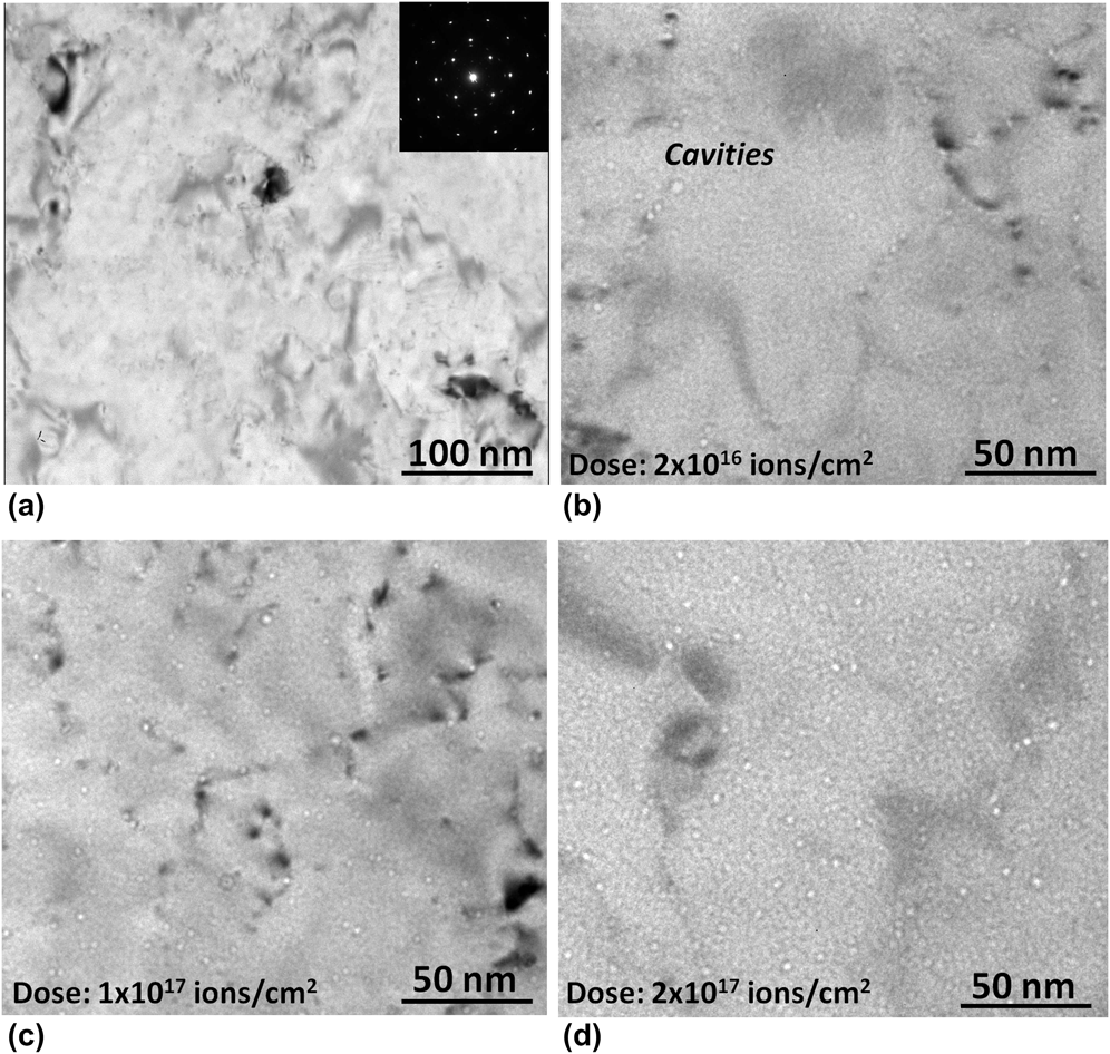
The microstructure of as-deposited and irradiated SC Cu film is displayed in Fig. 2. As shown in Fig. 2(a), the as-deposited SC film has clean structures and only dislocation contrast can be seen in some locations. The corresponding selected area diffraction pattern indicates that the Cu film has an SC structure with its image normal near [001]Cu. After He ion irradiation at 450 °C, visible cavities can be found in the SC film while the cavities number density varies a lot for different irradiation doses. Under irradiation to a dose of 2 × 10¹⁶ ions/cm2, cavities are distributed heterogeneously, with preferential nucleation along the growth defects, such as dislocations, as marked in Fig. 2(b). With the increase of dose to 1 × 10¹⁷ ions/cm2, some cavities are also observed away from dislocations as shown in Fig. 2(c). At the dose of 2 × 10¹⁷ ions/cm2, cavities appear to be distributed homogeneously [Fig. 2(d)], resulting from both heterogeneous and homogeneous nucleation of cavities across the sample in contrast to the cavities nucleated primarily at dislocations under lower dose irradiation [Fig. 2(b)]. These results indicate that the cavities number density increased with the irradiation dose, and the growth defects such as dislocation lines are preferential sites for nucleation of cavities in the SC Cu film under He irradiation.
TEM images showing the SC Cu film (a) prior to irradiation and after fluences of (b) 2 × 10¹⁶ ions/cm2, (c) 1 × 10¹⁷ ions/cm2, and (d) 2 × 10¹⁷ ions/cm2. The image in (a) is in focus, whereas those in (b)–(d) are taken under a defocus of −3 μm.
C. Irradiation damage of CG Cu
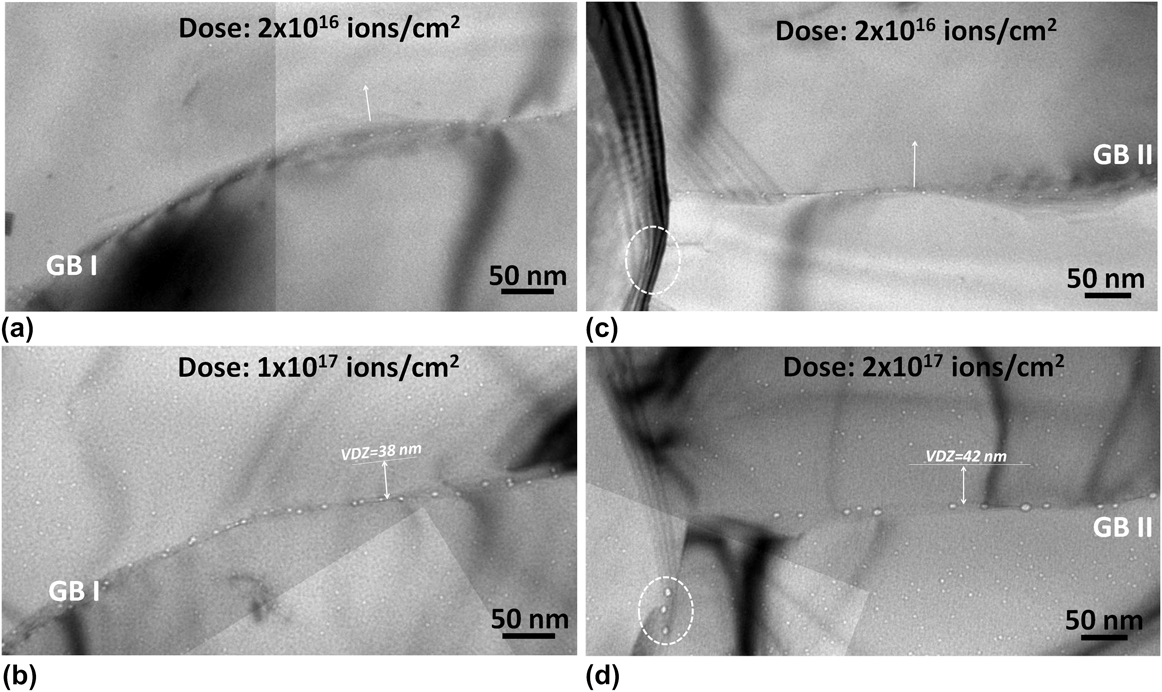
Figures 3(a)–3(d) show the irradiation damage features in the grain boundary regions in irradiated CG Cu with He ion fluences from 2 × 10¹⁶ to 2 × 10¹⁷ ions/cm2. A large number of irradiation-induced cavities were formed both in the grain interior and along grain boundaries. The cavities have a spherical shape with diameters smaller than ∼10 nm in grain interior. However, the cavities formed in the grain boundary are much larger than that in the grain interior as shown in Fig. 3. A clear VDZ can be identified along grain boundaries in Fig. 3, consistent with earlier reports.Reference Zhang, Huang, Millett, Tonks and Wolf29–Reference Zinkle35 Their presence indicates that grain boundaries are efficient sinks for irradiation-induced vacancies. Under the current elevated temperature irradiation conditions, no radiation-induced dislocation loops or stacking-fault tetrahedra were observed.
Irradiation damage near grain boundary I in CG Cu under fluences of (a) 2 × 10¹⁶ ions/cm2 and (b) 1 × 10¹⁷ ions/cm2. Irradiation damage near grain boundary II in CG Cu under fluences of (c) 2 × 10¹⁶ ions/cm2 and (d) 2 × 10¹⁷ ions/cm2. All images were taken with a defocus of −5 μm. VDZ stands for “void-denuded zone.” The dashed ellipse in (d) shows cavities that were not present at the lower dose shown in (c).
As revealed in a previous study, VDZ widths depend on the character of the grain boundaries along which they form.Reference Han, Demkowicz, Fu, Wang and Misra37 However, It is unclear whether a critical irradiation dose need to be achieved to form an obvious VDZs. Therefore, we performed irradiation on the same grain boundary and monitor the formation of VDZ under different fluences of He ions. As shown in Fig. 3, we found that the VDZs become clear with the increasing of irradiation dose. For grain boundary I, irradiated to a fluence of 2 × 10¹⁶ ions/cm2, no clear VDZ can be identified along the grain boundary [Fig. 3(a)] due to the low cavities density. In the mean time, some small cavities are nucleated and decorated along the grain boundary I. By increasing the dose to 1 × 10¹⁷ ions/cm2, the number of cavities near grain boundary I increased significantly, and the VDZ became obvious and has a width of 38 nm, and the size of cavities in grain boundary I become larger. These results show that a critical irradiation dose is needed to form a clear VDZ. A similar phenomenon can be observed in irradiated grain boundary II [Figs. 3(c) and 3(d)]. For irradiation with the dose of 2 × 10¹⁶ ions/cm2, no clear VDZ can be identified, such as no visible cavities can be found within 200 nm range in the upper part of grain boundary II [Fig. 3(c)], whereas there are many small cavities in the grain boundary interior. With the increasing irradiation dose, the VDZ becomes obvious and the width is ∼42 nm as marked in Fig. 3(d). Furthermore, as marked by the dashed circle in Fig. 3(d), cavities are formed in the left vertical grain boundary under high-dose irradiation, while not in the low-dose experiment shown in Fig. 3(c). These observations indicate that the grain boundaries are efficient sinks for vacancies, and a critical cavities density is needed to form clear VDZ.
D. Irradiation damage of NG Cu
The irradiation experiments in CG Cu show that the grain boundaries are efficient sinks for irradiation-induced vacancies, and the formation of clear VDZ need a critical cavities density. The typical widths are in the range of 40–70 nmReference Zinkle35 for general large-angle grain boundaries under He ion irradiation with a dose of 2 × 10¹⁷ ions/cm2. Hence, if the grain size is smaller than twice the width of VDZ, such as d < 80 nm, the cavities density in the grain interior would be expected to be reduced, and cavities will mainly nucleate along grain boundaries. Here, we have tested this hypothesis in NG Cu.
For the irradiation experiments performed on NG Cu, since the implantations were performed at 450 °C for ∼6 h, the grain size of NG Cu was significantly coarsened. As shown by the dark-field TEM image of the as-deposited NG Cu in Figs. 4(a) and 4(b), the initial grain size is ∼15 nm and has a relatively narrow size distribution. After irradiation at 450 °C to a dose of 1 × 10¹⁷ ions/cm2 by He ions, the average grain size increased to approximately 35 nm, with a wider size distribution from 15 to 60 nm, as displayed in Figs. 4(c) and 4(d). From the inserted selected area diffraction pattern in Figs. 4(a) and 4(c), we note that the continuous diffraction rings have become discontinuous consistent with an increase in grain size. Grain growth under irradiation is a phenomenon of interest to several applications, including the behavior of materials in nuclear reactors and the behavior of thin-film solid-state devices that are modified by ion implantation.Reference Wang, Thompson and Smeltzer49–Reference Alexander, Was and Rehn51 In general, the grain diameter is observed to increase linearly with the dose, and the grain boundary mobility increases linearly with deposited damage energy for a low-temperature regime (below about 0.15–0.22 T m), where grain growth is independent of the irradiation temperature.Reference Kaoumi, Motta and Birtcher52 For irradiation temperature higher than ∼0.3 T m, grain growth may be dominated by the thermally activated process.Reference Kaoumi, Motta and Birtcher52 In the current study, the irradiation temperature is ∼0.42T m-Cu, and hence the observed grain growth is primarily thermal. Irradiation to all three doses were performed at the same time by keeping all samples on the same heating stage and masking off some of them when they were irradiated to the desired dose (intend for easier experiment), and hence all the Cu film samples were kept at 450 °C for the same durations, so the extent of grain growth in three samples are identical. The quickly coarsening of the grain in irradiated NG Cu indicates the thermal instability of NG metals under high temperature irradiation.
(a) Dark-field TEM image and (b) grain size distribution of as-deposited NG Cu. (b) Dark-field TEM image of NG Cu after irradiation at 450 °C to a fluence of 1 × 10¹⁷ ions/cm2. (d) Grain size distribution of irradiated NG Cu in (c).
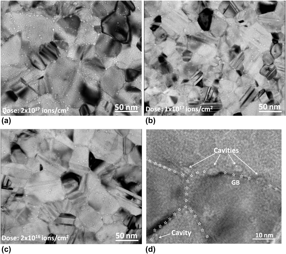
Figure 5 highlights the damage features of NG Cu irradiated at 450 °C with the same range of He ion doses as described above. As expected, few cavities are observed within grain interior since the grain size (∼50 nm or less after irradiation) is smaller than twice the characteristic widths of grain boundary VDZs shown in Fig. 3 and in Ref. Reference Han, Demkowicz, Fu, Wang and Misra37. Isolated cavities are observed within limited regions inside the specific grain interiors possibly due to the low sink efficiency of some nearby grain boundariesReference Zinkle35 or trapping of cavities by some local defects. Numerous cavities are nevertheless seen to form along the grain boundaries possibly due to the large fluxes of radiation-induced vacancies expected to arrive at the grain boundaries from the neighboring grains. Unlike cavities within grains, grain boundary cavities have an elliptical shape as shown in Fig. 5(d). Grain boundary triple junctions appear to be preferred sites for the formation of larger cavities. Some grain boundary cavities appear to grow preferentially toward one side of the grain boundary, which might be related to the orientation of the specific grains or grain coarsening after irradiation. It can be seen that there is a clear change in the number density and size of cavities with the decreasing dose. These results show that irradiation-induced cavities are mainly formed along grain boundaries in NG Cu, which is significantly different from its SC Cu and CG Cu counterpart. Our experimental studies clearly demonstrate that once the grain size is smaller than twice the characteristic width of grain boundary VDZ, the irradiation-induced defects mainly agglomerate along grain boundary sinks.
NG Cu irradiated to fluences of (a) 2 × 10¹⁷ ions/cm2, (b) 1 × 10¹⁷ ions/cm2, and (c) 2 × 10¹⁶ ions/cm2. (d) Elliptical cavities formed along grain boundaries in NG Cu irradiated to a dose of 1 × 10¹⁷ ions/cm2 (grain boundary contours are marked by white stars). (a)–(c) were taken under a defocus of −2 μm and (d) is in focus.
The size and number density of cavities formed in SC, CG, and NG Cu under the same ion irradiation conditions are compared in Figs. 6(a) and 6(b). The number density of cavities formed in SC and in grain interiors of CG and NG Cu are plotted in Fig. 6(a) as a function of irradiation dose. For the dose range investigated here, the number density of cavities in NG Cu is smaller than that in SC and CG Cu. In addition, the average size of cavities is smaller in NG Cu. With decreasing dose, the number densities of cavities decrease in irradiated SC, CG and NG Cu, as shown in Fig. 6(a). With increasing dose, the average radius of cavities formed in grain boundaries slightly increases for both CG and NG Cu. In particular, the average radius of cavities in NG Cu is smaller than that in CG Cu as shown in Fig. 6(a). These results demonstrate that the number densities and sizes of cavities are slightly suppressed in NG Cu than in SC and CG Cu under the same irradiation conditions.
Comparison of the dose dependences of (a) the number density of cavities in SC Cu and in grain interiors of CG and NG Cu and (b) the average radius of cavities formed at grain boundaries in CG Cu and NG Cu.
In the current studies, we performed irradiation experiments directly on the TEM foils with thickness less than 100 nm, and the top and bottom surfaces of TEM foils are also sinks for irradiation-induced defects.Reference Hishinuma, Katano and Shiraishi53 However, all the SC, CG, and NG Cu foils in our experiments have the similar surface effect during irradiation, hence the observed irradiation damage difference in SC, CG, and NG Cu are mainly due to the appearance of grain boundaries and the increase of their density (reduction in grain size). Due to certain effect of the free surface, the cavities formation will be less than what would occur in a thick bulk sample.Reference Hishinuma, Katano and Shiraishi53 Due to the large area per unit volume of grain boundaries in NG Cu, radiation-induced vacancies will largely migrate to grain boundaries. We expect that a significant fraction of those vacancies may annihilate with interstitials or with grain boundary defects, while the remaining excess vacancies (interstitials are easy to diffuse to dislocations, grain boundaries or free surface) agglomerate and form into cavities along grain boundaries. In this case, the total cavities number density and size is reduced obviously in NG Cu. However, in SC and CG Cu foils, only a smaller portion of irradiation-induced vacancies migrate to the grain boundaries and annihilate with interstitials or agglomerate into cavities. Most of the irradiation-induced vacancies remain inside grain interiors and contribute to cavities growth. Hence, the number density and the size of cavities in SC Cu and CG Cu are larger than in NG Cu. The current experimental studies demonstrate that synthesis of materials in the nanocrystalline form is moderately effective for suppressing irradiation-induced void-swelling. Furthermore, the thermal instability of NG Cu demonstrated in this study is one of the common drawbacks in nanocrystalline metallic materials, and the coarsening of the microstructures would be more significant in irradiated bulk NC Cu.
IV. CONCLUSIONS
Irradiation damage was investigated in SC, CG, and NG Cu exposed to He ion irradiation at elevated temperature. In SC Cu, plenty of cavities are nucleated and some of them are preferentially decorated along the growth defects and dislocations. In irradiated CG Cu, VDZs can be identified near most of the grain boundaries. In contrast, irradiation-induced cavities are observed predominantly along grain boundaries in NG Cu and less in the grain interior. The number densities and average size of cavities are smaller in NG Cu than in SC and CG Cu under the same irradiation conditions, suggesting a suppression of void-swelling.
ACKNOWLEDGMENTS
This work was supported by the Center for Materials in Irradiation and Mechanical Extremes (CMIME), an Energy Frontier Research Center (EFRC) funded by the US Department of Energy, Office of Science, Office of Basic Energy Sciences under Grant No. 2008LANL 1026. The authors thank J.K. Baldwin at the Center for Integrated Nanotechnologies at LANL, a Basic Energy Science sponsored user facility, for film deposition.