I. INTRODUCTION
Silicon carbide has been identified as an outstanding material for micro-electro-mechanical systems due to its mechanical durability, chemical inertness, and electrical stability.Reference Krotz, Legner, Wagner, Moller, Sonntag and Muller1–Reference Tong, Mehregany and Matus3 These properties make silicon carbide a better choice than silicon for pressure sensors designed to operate in the harsh environments associated with aerospace, advanced industrial process control, and automotive applications.4 Development of micromachined SiC pressure sensors for high temperature applications has historically focused on devices based on piezoresistive sensing.Reference Ned, Okojie and Kurtz5–Reference Wu, Stefanescu, Kuo, Zorman, Mehregany and Obermeier9 Since typical piezoresistive sensing elements are in the form of conductive wires and a separate entity from the pressure holding diaphragm, the implementation of piezoresistive sensing structures usually requires additional processing steps to assemble and form the encapsulated reference pressure chamber for pressure sensing purposes. In addition, piezoresistive pressure sensors typically exhibit a strong temperature dependence. The strong dependence on material properties, piezoresistivity in particular, confines design flexibility and also necessitates in situ calibration to maintain device performance.Reference Hammerschmidt, Schnatz, Brockherde, Hosticka and Obermeier10 More importantly, such pressure sensors are typically made of single crystalline material to realize sufficiently high gauge factors (GFs) for practical use, especially at high temperatures. The GF of 6H–SiC is 41.5 (absolute value; applicable throughout the text), which is only a small fraction of its n-type Si counterpart at about 133.Reference Shor, Bemis and Kurtz11, Reference Shor, Goldstein and Kurtz12 Compared with monocrystalline SiC, polycrystalline SiC has even lower GFs, ranging between 0.4 and 31.8.Reference Shor, Goldstein and Kurtz12, Reference Wu, Zorman and Mehregany13 In all cases, the GFs of crystalline SiC materials are expected to drop by at least 50% from their room temperature values for temperatures above 400 °C.Reference Shor, Bemis and Kurtz11–Reference Wu, Zorman and Mehregany13 The strong temperature dependence of the piezoresistvity in SiC affects pressure sensor performance at high temperatures and thus presents a significant challenge for implementing high sensitivity pressure sensing devices for operation in high temperature environments. The moderate high temperature GFs for piezoresistive SiC pressure sensors also result in a low signal-to-noise ratio necessitating the use of thermally tolerant conditioning circuits, which themselves are still under development.
In contrast to piezoresistive sensing, capacitive sensing is one of the few means to realize pressure sensors made from polycrystalline or amorphous materials. Capacitive pressure sensors are known to exhibit good sensitivity, mechanical robustness, and low turn-on temperature drift at room temperature.Reference Ko and Wang14, Reference Ko, Wang and Wang15 Capacitive devices ideally consume no DC power and are simpler in design than their piezoresistive counterparts. Furthermore, capacitive devices are well suited for interfacing with signal conditioning circuits. These advantages make capacitive sensing a promising approach for applications where space, design flexibility, and power consumption are of principal importance, as would be required in many high temperature environments. In addition, wireless high temperature pressure sensing and telemetry can be readily implemented with capacitive sensors and thus provide value-added features to existing transduction systems.Reference Fonseca, English, von Arx and Allen16 Previously, we reported the development of a high temperature (400 °C) capacitive pressure sensor made from an epitaxially grown single-crystal 3C–SiC thin film diaphragm and fabricated by wafer bonding.Reference Young, Du, Zorman and Ko17 However, high residual stresses (>200 MPa) in the epitaxial films and the resultant excess curvature of the Si substrate adversely affected the transfer yield during wafer bonding, especially for 3C–SiC film thicknesses greater than 0.5 μm, thus limiting the operable pressure range.
A solution to the limitations associated with 3C–SiC is to replace the single crystalline 3C–SiC films with low stress, nitrogen-doped, polycrystalline 3C–SiC (poly-SiC) films. The low residual stress in these films would greatly facilitate wafer bonding and thus enable diaphragms of greater thicknesses be used. We reported earlier preliminary test data of the proof-of-concept devices with performance demonstrated up to 400 °C.Reference Du, Ko, Mehregany and Zorman18 Such devices feature a poly-SiC-on-Si architecture that is fabricated by using a wafer bonding technique. Concurrent with our effort, a separate group developed a poly-SiC capacitive pressure sensing architecture with operating temperatures up to 574 °C.Reference Chen and Mehregany19, Reference Chen and Mehregany20 This sensor was fabricated by surface micromachining utilizing a poly-SiC film that was directly deposited onto the sensor substrate. For performance and process compatibility concerns, the micromachining approach demanded the poly-SiC diaphragms to be homogeneously integrated with a premium polycrystalline SiC substrate as its sensor substrate. Both these examples demonstrate the potential utility of poly-SiC as a pressure sensor material, especially with respect to process flexibility, essentially bringing poly-SiC on par with polysilicon.
In this paper, we detail the further development of a wafer-bonded poly-SiC-on-Si architecture for high temperature capacitive pressure sensing. Included in this investigation was a study of the oxidation behavior of poly-SiC and how it relates to the wafer bonding process. To identify practical operation limits, the sensors were tested in a nitrogen-filled and custom-built chamber up to 500 °C. The test results were then analyzed to relate the observed performance with its underlying material properties and device architecture.
II. CAPACITIVE PRESSURE SENSING ARCHITECTURE BASED UPON POLY-SiC THIN FILM DIAPHRAGMS
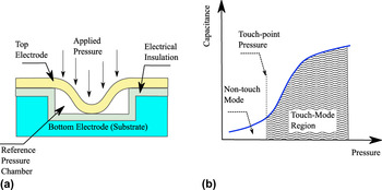
The sensor developed in this study was designed to operate as a touch mode capacitive pressure sensor and was based on a design first implemented in silicon and detailed elsewhere.Reference Chen and Mehregany20Figures 1(a) and 1(b) show a cross-sectional view of the capacitive sensor architecture and an illustration of the main operation modes, respectively. The basic device consists of an edge-clamped circular poly-SiC diaphragm suspended over a micromachined sealed vacuum cavity. The sealed vacuum cavity provides a pressure reference, and when its internal pressure approaches zero, the capacitive sensor essentially measures absolute pressure [Fig. 1(a)]. The device behavior can be empirically divided into different operational modes according to the load condition of the sensing diaphragm. When an external pressure is applied, the diaphragm deflects toward the base of the cavity, thus increasing the device capacitance value as shown in Fig. 1(b). When the external pressure increases to the touch-point pressure, the diaphragm makes contact with the base of the sealed cavity causing a steep nonlinear increase of capacitance. As the pressure is increased further into the touch mode zone, sufficient contact is made to linearize the capacitance output. The load–deflection behavior within a certain range of pressure beyond the touch-point pressure is nearly linear, and this behavior gives the sensor a higher sensitivity than when operated in the nontouch mode regions.Reference Ko and Wang14
The concept of microscale capacitive pressure sensing: (a) cross-sectional view of the capacitive pressure sensing architecture showing touch mode operation and (b) operating modes of the sensor.

A wide range of operating pressures can be realized by choosing device dimensions using the following equation:
 $$P_{\rm{T}} = {{{\rm{64}}D} \over {a^{\rm{4}} }}g + {{({\rm{1}} + \nu )({\rm{23}} - {\rm{9}}\nu ){\rm{8}}Dg^{\rm{3}} } \over {{\rm{7}}a^{\rm{4}} h^{\rm{2}} }} + {{{\rm{4\sigma }}h} \over {a^{\rm{2}} }}g\quad,$$
where P T, a, h, g,  ${\rm{\sigma }}$, v, and D are the touch-point pressure, diaphragm radius, film thickness, cavity depth, film residual stress (in-plane), Poisson’s ratio, and flexural rigidity, respectively.Reference Eaton, Bitsie, Smith and Plummer22, Reference Timoshenko23 In fabricating capacitive pressure sensors, wafer bonding offers a distinct advantage over surface micromachining from a design perspective in that the bonding process enables a much wider range of cavity depths than is practically achievable by surface micromachining.
III. FABRICATION PROCESS DEVELOPMENT
A. Preparation of polycrystalline 3C–SiC thin films
Conductive highly oriented (111) poly-SiC films with low tensile stresses were deposited on 100-mm-diameter (100) silicon substrates in a high throughput low-pressure chemical vapor deposition (LPCVD) furnace detailed elsewhere.Reference Dunning24 The deposition process used SiH2Cl2 (DCS) and C2H2 (5% in H2) precursor gases as Si and C sources, respectively. In addition, NH3 (5% in H2) was used as a n-type doping gas.Reference Trevino, Xiao-An, Mehregany and Zorman25 Poly-SiC films were deposited onto the front sides of the silicon substrates at a deposition pressure of 4 Torr with a fixed deposition temperature of 900 °C by setting a constant flow of DCS at 35 sccm, C2H2 at 180 sccm, and NH3 at 64 sccm. To minimize contamination and ensure deposition quality, a standard RCA clean was performed on each substrate before poly-SiC deposition.
B. Oxidation behavior of polycrystalline 3C–SiC thin films
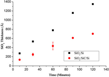
The oxidation behavior of the LPCVD poly-SiC films was investigated for two reasons: (i) to determine whether thermal oxides grown directly on the poly-SiC films could be used as bonding layers in device fabrication and (ii) to experimentally examine the oxidation resistance of the films. To minimize the effect of surface morphology on oxidation, the poly-SiC films were polished down to a surface roughness of about 2 nm using a polishing technique discussed later in this paper. A series of oxidation experiments with variable oxidation time were performed at 1050 °C with a constant oxygen flow of 6 sccm. A 30-min postoxidation anneal was performed at the same temperature in an inert environment by purging a constant nitrogen flow of 10 sccm. The silicon dioxide thicknesses were measured using an ellipsometer. For ultrathin oxide films grown from very short oxidations, atomic force microscopy (AFM) was used instead to obtain the thickness information by measuring the height of the oxide steps formed by patterning the oxide films. Oxides grown on Si (100) wafers under the same oxidation conditions were used as reference samples. The experimental results are presented in Fig. 2. As expected, the oxidation rate of the poly-SiC films is much slower than that of single-crystal silicon. For most oxidation times, the oxide thickness on the poly-SiC film is thinner than that of silicon by a factor of two. Nevertheless, the oxide films were continuous even for short oxidation times, and the data suggest that oxides of sufficient thickness to serve as a bonding layer and for dielectric isolation can be grown by thermal oxidation of the poly-SiC films.
Oxidation behavior of (100) Si and (111) poly-SiC thin films.

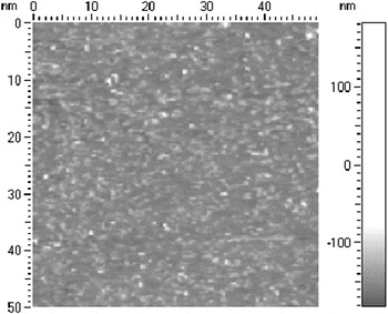
AFM was used to characterize the surface morphology of the as-grown thermal oxides. Figure 3 shows an AFM micrograph from a thermal oxide grown during the 10-min oxidation run. The average surface roughness of the polished poly-SiC thin film before oxidation was below 2 nm, while the surface roughness of the 13-nm-thick oxide was 17 nm, over eight times higher. For Si wafer bonding, this level of surface roughness is too high for successful fusion bonding, requiring a postoxidation chemical mechanical polishing (CMP) step to reduce the roughness to acceptable levels.
AFM micrograph of the surface of a thermal oxide film grown on a poly-SiC thin film. The average surface roughness (R a) is 17 nm.

Although not definitive due to the limited scope of the oxidation study, the data in Fig. 2 do suggest that at high temperatures in extremely oxidizing environments, the resulting oxide layer on poly-SiC will be in the 100-nm range. For thin diaphragms, such passivation layer thicknesses can be incorporated into the design of the pressure sensor by accounting for their affect on the mechanical performance of the diaphragm. For thick diaphragms, such oxides will be too thin to be relevant mechanically.
C. Wafer bonding process development
To create a touch mode poly-SiC capacitive pressure sensor, a wafer bonding process was developed to form the vacuum-sealed cavity in the device architecture. Wafer bonding enables the fabrication of diaphragms with a wide range of diameters, especially large diameter diaphragms not easily implementable using other methods. In addition, wafer bonding greatly simplifies the fabrication processes, resulting in a potential reduction of fabrication cost.
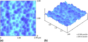
Successful wafer bonding relies on smooth contact surfaces and reliable postbonding annealing. As shown in Fig. 4, the LPCVD poly-SiC films are inherently rough due to the faceted nature of the grains. To address this issue, a two-step CMP process was developed to prepare poly-SiC films for wafer bonding. Both steps used a 1:20 colloidal silicon dioxide slurry diluted in deionized water. A hard urethane composition polishing pad and a soft nap fabric polishing pad were applied in the first and the second steps, respectively. A clamping force of 300 N was applied throughout the polishing process. Poly-SiC was removed at a rate of 4 nm/min in the first step and less than 5 nm in total during the second step as it was a refining process. AFM analysis showed that the two-step polishing can reduce the surface roughness (R a) of the poly-SiC films from 20 to ∼2 nm.
Typical AFM micrographs from an arbitrarily chosen fragment of as-deposited LPCVD poly-SiC. The average surface roughness (R a) is about 20 nm: (a) a surface topography image and (b) a three-dimensional height image of the surface.

Use of thermally grown SiO2 on the poly-SiC films in the wafer bonding process was evaluated by way of SiO2/Si or SiO2/SiO2 bonding interfaces. Though the surfaces of both the poly-SiC and the SiO2 films were thoroughly polished using the two-step SiC polishing recipe and a standard SiO2 polishing recipe that could yield a smooth surface sufficient for wafer bonding, little success was observed (<5% bonded area) for any combination when the bonded pair was annealed at 1000 °C. Separation along the bonding interface after the postbonding anneal was very common, although the two substrates could be bonded initially in some cases. The low yield may be due to the thermal mismatch-induced debond during the annealing processReference Tong, Gosele, Yuan, Steckl and Reiche26 that prevents the formation of covalent bonds between the layers combined with excessive surface roughness, which limits contact area. To address this issue, a phosphosilicate glass (PSG) to silicon bonding process was developed instead to take advantage of the reflow characteristics of PSG. The idea of PSG reflow process is to use the PSG as an intermediate layer and subject it to a temperature sufficiently high to undertake a viscous deformation. The reflow process is believed to help promote the formation of covalent bonds.Reference Kern and Schnable27 The use of PSG significantly increased the wafer bonding yield resulting in a repeatable transfer yield of poly-SiC films greater than 70%.
D. Pressure sensor process integration
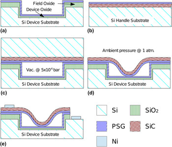
The capacitive pressure sensors were fabricated using a wafer-scale PSG reflow-based bonding process illustrated schematically in Fig. 5. A 100-mm-diameter heavily doped n-type Si “device” wafer was first thermally oxidized to form a 1.5-μm-thick oxide layer on its exposed surfaces. Windows were patterned into the oxide on the top surface, and the exposed Si was etched by reactive ion etching (RIE) to form cavities of various diameters and 8–10 μm in depth. A 100-nm-thick dry thermal oxide was then grown on the exposed Si surfaces of the cavities. After the second oxidation, the area right under the suspending diaphragm was covered by the 100-nm-thick oxide (“device oxide”), while the rest of surfaces parallel to the “device oxide” surface was padded with oxide thicker than 1.5 μm (“field oxide”). Since capacitance is inversely proportional to insulation thickness, this two-step oxidation process helps to minimize parasitic capacitances while maintaining reasonable device sensitivity [Fig. 5(a)]. Next, a 1-μm-thick heavily doped (0.02 Ωcm) low stress (≤100 MPa) poly-SiC film was deposited on a 100-mm-diameter Si “carrier” wafer by LPCVD using the deposition process discussed earlier. The as-deposited poly-SiC film was then polished to a roughness of about 2 nm using the two-step CMP process described previously. A 150-nm-thick PSG film was then deposited on both the carrier and device wafers by LPCVD [Figs. 5(a) and 5(b)]. The two PSG surfaces were then polished, cleaned, and bonded in a commercial vacuum bonding tool (EVG EVG501 Wafer Bonding System™, Tempe, AZ) using an applied force of 1500 N and a chamber pressure of 5 × 10⁻⁶ bar. The bonding system sustained the vacuum level and applied force throughout the bonding process till the bonding surfaces were firmly and hermetically joined to seal the cavities [Fig. 5(c)]. If out-gassing from any postbonding activities is negligible, the vacuum status in the sealed cavities shall be maintained; hence, the internal pressure of the sealed cavity has little effect on the normal operation of the sensor upon temperature increase considering the ideal gas law. For instance, even at 500 °C, the internal pressure of the sealed cavity is expected to be merely about 13 × 10−6 bar [1.9 × 10⁻⁴ pounds per inch absolute pressure (PSIA)], which is de facto an infinitesimal fraction of the operation pressure of interest. The bonded pair was then annealed at 1000 °C in nitrogen for 2 h to enhance the bond strength and to facilitate PSG reflow. The PSG layer plays a role as both an electrical insulation layer and a wafer bonding interface layer, and the reflow process facilitates the formation of a uniform bonding interface and hence a uniform insulation layer. The Si carrier wafer was then dissolved in tetramethylammonium hydroxide (TMAH), resulting in the transfer of the poly-SiC film to the patterned device wafer [Fig. 5(d)]. Following the TMAH-etch, the transferred poly-SiC film was patterned by RIE using a CHF3/O2 plasma. A contact window to the substrate was subsequently etched in a time-controlled manner using the same plasma etching system. A 1-μm-thick Ni film was then sputter deposited onto the “device” wafer and photolithographically patterned to define the upper and lower electrodes [Fig. 5(e)]. The patterned Ni contact pads were then annealed at 700 °C in a nitrogen-purged furnace for 2 h to form stable high temperature ohmic contacts.Reference Okojie, Ned and Kurtz7
Cross-sectional views of the capacitive pressure sensor fabrication process using LPCVD poly-SiC films: (a) construct reference pressure chamber; (b) deposit SiC and PSG; (c) hermetic seal reference pressure chamber via wafer bonding; (d) release sensing diaphragm; and (e) form contact pads.

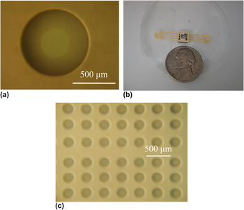
Figure 6 presents a plan-view optical micrograph of a capacitive pressure sensor that incorporates an 800-μm-diameter diaphragm. The optically transparent SiC diaphragm, which is at the center of the picture, is electrically isolated from the remainder of the chip by a ring-shaped trench (not shown). The diameter of the isolation ring was designed to be considerably larger than the diameter of the SiC diaphragm to allow sufficient mechanical anchoring that is essential for wafer bonding-based pressure sensor fabrication. It should be noted that the cavity depth was intentionally made at least eight times the thickness of the sensor diaphragm to evaluate the durability of the sensing diaphragm at various high temperatures. Each sensor was packaged by first dicing the device wafer into chips and sintering each chip onto a ceramic flat pack packaging socket with gold-plated leads using a high temperature ceramic paste. Each socket was then wire bonded to the contact pads of the sensor for testing. A photograph of a sensor packaged for high temperature testing as well as a dense array of 100-μm-radius sensors are also shown in Fig. 6.
Plan-view photographs of poly-SiC capacitive pressure sensors: (a) an 800-μm-diameter sensor diaphragm in touch mode operation, (b) a sensor die packaged for high temperature testing, and (c) an array of 100-μm-radius poly-SiC capacitive pressure sensors. The lightly shaded region in (a) is due to the diaphragm making contact with the sensor cavity when in the touch mode.

IV. EVALUATION OF THE SENSING PERFORMANCE
A. Test environment and method
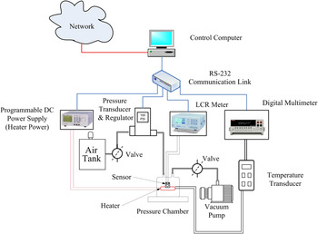
Device performance was characterized in a custom-built high temperature testing chamber. To minimize measurement errors and enable stable device monitoring capability, an automated measurement system was utilized. A schematic of such a system is presented in Fig. 7. Automated pressure regulation was implemented by a single-valve digital pressure regulator and transducer assembly with a resolution of ±0.05 PSI operable at both vacuum and positive pressures. Capacitance was measured by a LCR [Inductance (L), Capacitance (C), and Resistance (R)] meter with accuracy of 1% or better. A high power density boron nitride ceramic heater was used for substrate heating. To minimize capacitive interference caused by AC glitches, a high voltage programmable DC power supply with a resolution of 20 mV was used to power the ceramic heater. Temperature was monitored in real time by a temperature transducer that was capable of transmitting the temperature information as a DC voltage signal to an uplink multimeter. The multimeter collected and relayed the temperature readings to a computer that implemented a proportional?integral?derivative (PID) control algorithm to maintain the temperature to within ±2 °C of the set point by tuning the output voltage of the programmable DC power supply. The operation temperature of the pressure test chamber could be maintained as high as 500 °C using this setup.
The automated pressure sensor characterization system.

Devices were tested under positive pressures between 400 and 500 °C. The test pressure started from 15.5 PSIA to let the device operate in high sensitivity touch mode. To isolate the sensor capacitance from the inherent parasitic impedances, a dual frequency measurement methodReference Yang28 was applied while toggling the test frequency between 50 and 100 kHz. Pressures were ramped both up and down with a step size of 0.5 PSIA. To maintain static testing conditions for each measurement, the applied pressure was allowed to stabilize for 60 s before a reading was taken. A total of four readings were obtained for each test point. Under these test conditions, the device was subjected to pressure loading at 500 °C for about 3 h excluding the heating and cooling times.
B. Test results
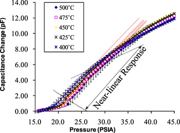
Figure 8 presents representative high temperature capacitive pressure sensing behavior for a 0.8-mm-diameter sensor. The applied pressure, expressed in terms of absolute pressure (PSIA), ranges from 15.5 to 45 PSIA. The capacitance change is referenced to the capacitance reading at an applied pressure of 15.5 PSIA. As the boundary between the touch mode and the nontouch mode operations, i.e., the touch-point pressure was calculated to be at about 8 PSIA for room temperature operation, setting the start pressure far from the mode boundary ensured that the sensor operated in its touch mode with sufficiently significant responses at all test temperatures under the stated test conditions.
Measurements of capacitance change as a function of applied pressure for temperatures between 400 and 500 °C. Dash lines denote linear regression fitted tangents to the sensing curves. The near-linear response segments of the sensing curves are indicated in the graph.

It has been first disclosed with silicon membranes that at room temperature, the capacitive pressure sensing responses in touch mode have a nonzero curvature or are piecewise linear. Within some selected ranges, however, segments with near-linear responses could be identified.Reference Ko and Wang14, Reference Wang21 The near-linear response is preserved in SiC materials as reported in literature,Reference Young, Du, Zorman and Ko17–Reference Chen and Mehregany20 and similar behavior is found in the high temperature operation of our poly-SiC membranes. In Fig. 8, a cluster of such segments is marked by dash lines. These lines are tangents to the linear segments of the sensing curves and were determined by linear regression. The overlap between each linear segment of the sensing curve and its tangent defines the linear operation range. In Fig. 8, the two dense dash lines demarcate the full-scale linear range (FSLR) of each sensing curve at its test temperature. At 400 °C, the linear range is between 21.1 and 26.3 PSIA. The linear range migrates to be between 22.2 and 31.2 PSIA at 500 °C. The nonlinearity is 3% FSLR or better for all the sensing curves. The tangent lines are visually near parallel to each other indicating a near constant sensitivity across all test temperatures. The observation can be quantitatively verified by noting the values of sensitivity. The sensitivity is 0.62 pF/PSIA at 400 °C and changes to 0.53 pF/PSIA at 500 °C, which is a 14.5% drop in response to the 25% temperature increase.
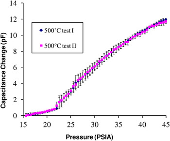
To test the performance drift at 500 °C, the sensor was subjected to a separate 500 °C duty cycle sequence performed on another day. Between the first and second test sequences, the sensor was allowed to cool down to room temperature and be fully disengaged from the inert environment. Figure 9 compares the 500 °C measurements obtained from these two separate test sequences. The two sensing curves, though from two uncorrelated test sequences, are conformal to each other. The largest deviation is seen at 45.0 PSIA where the average capacitance readings differ by only 0.27 pF. For a full-scale range between 15.5 and 45.0 PSIA, the 0.27 pF difference accounts for about 2% performance drift.
Repeatability of pressure sensing performance at 500 °C as demonstrated by data from two independent tests performed on separate days.

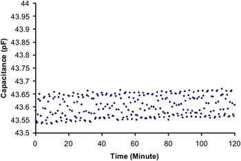
For a high temperature pressure sensor, thermal noise becomes a prominent factor that affects sensor resolution as the temperature approaches the maximum operating range. To quantify the sensor resolution at high temperatures, a thermal test was performed on the sensor at a fixed pressure of 2.9 PSIA and a temperature of 450 °C. At a pressure of 2.9 PSIA, the sensor diaphragm is far from the high sensitivity range and thus insensitive to external pressure changes. Thus, any discernable capacitance variation is primarily due to thermal perturbations to the entire test environment. A total of 270 data points were collected in an interval of 120 min and the results are shown in Fig. 10. The measurement uncertainty, expressed as the standard deviation of the capacitance reading at a fixed pressure, is approximately 39 aF. This corresponds to a measurement-related sensor resolution of 0.68 PSIA.
Resolution of the capacitive pressure sensor as determined by thermal noise measurements performed at 450 °C.

V. CONCLUSIONS
A LPCVD poly-SiC diaphragm-based capacitive pressure sensing architecture, including single diaphragm sensors as well as sensor arrays, was developed using wafer bonding. The use of wafer bonding significantly decreases the complexity of fabrication process especially the vacuum cavity sealing procedure. The oxidation behavior of the LPCVD poly-SiC thin films was studied to evaluate their utility as a bonding layer as well as the anticipated chemical durability of the poly-SiC films in highly oxidizing environments. The oxidation study and consequent bonding experiments suggest that the thermal oxide grown on poly-SiC is not suitable for wafer bonding in the context of sensor integration. The developed CMP and PSG reflow processes are crucial for the success of wafer bonding and device integration. A fabricated pressure sensing prototype was tested at high temperatures between 400 and 500 °C. With a diameter-to-thickness ratio of 800 and a maximum deflection up to eight times its thickness, the poly-SiC pressure sensor demonstrated stable and repeatable sensing performance up to 500 °C. The demonstration of the high temperature operation of the presented architecture verifies that highly conductive LPCVD poly-SiC thin films with low tensile stress are suitable for high temperature harsh environment pressure sensing applications. Further, the fact that the poly-SiC thin films can be heterogeneously integrated with silicon substrates via wafer bonding could prove to be a viable platform for building diaphragm-based transducers; and the demonstrated high temperature pressure sensing capability up to 500 °C indicates that the proposed poly-SiC-on-Si architecture is feasible for high temperature environment sensing. Since the Si substrate material is not crucial to the sensor design, the demonstrated wafer-bonded sensing architecture could be adapted to other substrates, including those well suited for harsh environment applications, such as alumina and other polytypes of SiC, thus bringing the outstanding properties of poly-SiC to substrates that are not well suited for direct growth of poly-SiC.
ACKNOWLEDGMENTS
The authors would like to thank Professor Wen H. Ko and Professor Mehran Mehregany with the EECS Department at Case Western Reserve University for constructive discussions. The authors gratefully acknowledge Mr. Ron Jezeski for maintaining the LPCVD deposition systems. Group member Allison Hess contributed the program code, which was later revised and enriched for the automated test setup. Andeen-Hagerling Inc. in Cleveland, OH, provided equipment for capacitance calibration. Device fabrication was performed in the Center for Micro- and Nano-Processing at Case Western Reserve University. This research was supported by the National Science Foundation under Grant No. ECS 0367274.