I. INTRODUCTION
Oxide composites are a vital class of materials for a wide variety of applications. Nanomaterials primarily differ from their bulk counterparts through an increased density of interfaces. Many properties of materials are often attributed to the interaction of atomic scale defects with interfaces. This is especially true for those properties related to defect mobilities, such as radiation tolerance.Reference Weber, Ewing, Catlow, Diaz de la Rubia, Hobbs, Kinoshita, Matzke, Motta, Nastasi, Salje, Vance and Zinkle1 For example, ceramic–matrix composite materials,Reference Ajayan2 similar in morphology to carbon-based ceramic composites,Reference Xia, Riester, Curtin, Li, Sheldon, Liang, Chang and Xu3,Reference Peigney, Laurent, Flahaut and Rousset4 are under consideration for next generation nuclear energy fuel designs,Reference Yamawaki, Yamaguchi and Suzuki5 self-healing laminates for deep space exploration,Reference Voevodin and Zabinski6,Reference Eberly, Ou, Karcz and Skandan7 and superhard coatings for low friction applications.Reference Zhang, Sun, Fu and Du8,Reference Birkholz, Albers and Jung9 Applying advanced materials characterization to expose the interaction of point defects with interfaces is vital for understanding and exploiting the utility of composites in each of these applications.
Tailoring composites materials and their inherent abundance of interfaces is one of the many plausible ways to mitigate the effects of point defect accumulation and improve on the radiation tolerance of materials. In damage studies, radiation tolerance has often been attributed to the interactions between defects and interfaces.Reference Rubloff10,Reference Chiang, Lavik, Kosacki, Tuller and Ying11 The associated mobilities of defects are further dictated by the structure and chemistry of the material. As a consequence, avoiding the formation of radiation-induced phases and retaining structural rigidity by mitigating the build up of radiation-induced point defects are current concerns. In previous works, the high density of interfaces offered by nanometallic multilayer systems led to a substantial enhancement to radiation tolerance.Reference Misra, Demkowicz, Zhang and Hoagland12–Reference Han, Misra, Mara, Germann, Baldwin, Shimada and Luo14 Conversely, Valdez et al.Reference Valdez, Usov, Won, Tang, Dickerson, Jarvinen and Sickafus15 and Usov et al.Reference Usov, Valdez, Won and Devlin16 synthesized ceramic–matrix nanocomposites, irradiated them with 10 MeV Au, and observed improved resistance to both radiation-induced swelling and embrittlement. Ultimately, they showed that MgO/HfO2 interfaces acted as thermodynamic traps that showed virtually no build-up of damage. Similarly, Shen et al.Reference Shen, Feng, Tang, Valdez, Wang and Sickafus17 observed that MgGa2O4 with small sub-10 nm domains did not amorphize up to doses of 96 displacements per atom (dpa), yet the same material with larger domains irradiated under the same conditions readily amorphized by 12 dpa. These results demonstrate the enhanced radiation tolerance that can be afforded by interfaces. Meldrum et al.Reference Meldrum, Boatner and Ewing18, however, found that ZrO2 readily amorphized more easily than SiO2 under irradiation of SiO2/ZrO2 composites, an effect which was attributed to the differences in defect mobilities. More surprisingly, in this composite structure, ZrO2 amorphized while in single phase nanocrystalline form, ZrO2 could not be amorphized.Reference Meldrum, Boatner and Ewing18 More recently, we have examined the radiation damage evolution at oxide/oxide interfaces for a series of composites containing SrTiO3 (STO). Previous work on STO has been primarily focused on the amorphization behavior of single crystalline STO,Reference Oyoshi, Hishita and Haneda19,Reference Nakao, Wang, Jin, Miyagawa and Miyagawa20 such as the work by Zhang et al.Reference Zhang, Lian, Wang, Jiang, Ewing and Weber21 where they determined the kinetics of amorphization and recrystallization under electron irradiation at room temperature. Such studies have established that the amorphization of STO is very sensitive to the ion beam parameters, particularly electronic stopping effectsReference Meldrum, Boatner and Ewing22 and the dose rate.Reference Zhang, Lian, Wang, Jiang, Ewing and Weber21 However, how neighboring phases influence the amorphization susceptibility of a material such as STO has not received extensive attention. We have found in our recent studies that the radiation response of STO is very sensitive to both the nature of the other phase present in the compositeReference Zhuo, Uberuaga, Yan, Fu, Dickerson, Wang, Misra, Nastasi and Jia23–Reference Bi, Uberuaga, Vernon, Aguiar, Fu, Zheng, Zhang, Wang, Misra and Jia26 as well as the structure of the interface itself.Reference Aguiar, Dholabhai, Bi, Jia, Fu, Wang, Aoki, Zhu, Misra and Uberuaga27 In spite of this large body of work, however, there remain significant uncertainties involving the fundamental origins of enhanced radiation tolerances and overall phase stability under irradiation in nanostructured oxides.
The importance of studying defect–interface interactions is critical to maximize the utility of composites. Interfaces are generally considered regions for defects to migrate to or avoid, but their roles during irradiation are also dependent on the type of defect and neighboring energetics.Reference Uberuaga, Martinez, Bi, Zhuo, Jia, Nastasi, Misra and Caro25 Resolving localized defect–interface interactions in a composite requires an extended consideration of an assortment of structural, chemical, and synergistic effects between the two. With a focus on resolving salient material phenomenon, the use of model material bilayer systems that can be readily synthesized, characterized, and irradiated are of vital importance. Following the characterization of model material systems, the defect evolution and phase stability can be easily assessed through the use of controlled ion irradiation experiments and that behavior generalized to understand more complex composite structures.
In this study, we apply this model approach and use sub-Ångström scaleReference Nellist, Chisholm, Dellby, Krivanek, Murfitt, Szilagyi, Lupini, Borisevich, Sides and Pennycook28 microscopy to study the defect evolution of an oxide bilayer, STO/MgO, comprised of both STO (100) and (110) domains, under irradiation. Within these two domains, we focus our study on the susceptibility to amorphization and subsequent phase evolution following irradiation. Based on our microscopy results, we find that STO domains with a (110) domain orientation on MgO (100) have a greater susceptibility to amorphization compared with STO (100) domains. We attribute the behavior to the differences in interface structure and how defects at those interfaces interact with the rest of the domain. In particular, in STO (110), the alternating layers are electrostatically charged and thus interact with any charges formed at the interface. Following increasing fluence, microscopy results further reveal the emergence of an amorphous-to-crystalline transition in the vicinity of the original STO/MgO interface. This behavior alludes to the evolutionary nature of irradiated oxide interfaces. In summary, our study provides critical insights into the effect of termination chemistry, the evolution of ceramics, and the role of interface structure on the evolution of phase stability following ion bombardment at oxide interfaces.
II. EXPERIMENTAL DESIGN AND METHODS
To grow and characterize bilayer interfaces, we used pulsed laser deposition (PLD), ion irradiation, and atomic scale microscopy. With an emphasis on exposing changes in structure, defect chemistry, and their associated mobilities at and near interfaces, aberration corrected scanning transmission electron microscopy (STEM)Reference Krivanek, Dellby and Lupini29 was well suited to discern materials with single atom sensitivity.Reference Muller, Nakagawa, Ohtomo, Grazul and Hwang30 Combining experimental techniques for growth, irradiation, and STEM thereby offers a detailed approach to study point defect evolution within oxide bilayers.
A. Synthesis and characterization
To study the physical evolution of model interfaces following ion irradiation, epitaxial thin films of STO were first grown on single-crystal commercial MgO (100) substrates by PLD with a KrF excimer laser (Lambda Physik, λ = 248 nm). The laser beam with an energy density of approximately 3.5 J/cm2 was focused onto the target at an incidence angle of 45°. Prior to the deposition, the chamber was evacuated to a base pressure of 1.5 × 10⁻⁶ Torr or better. An optimized substrate temperature of 700 °C and oxygen pressure of 150 mTorr were used during the depositions. The films were deposited at 2 Hz repeat ion rates. After deposition, the films were cooled down to room temperature at an oxygen pressure of 1 Torr to assure proper film oxidation.
Following growth, x-ray diffraction (XRD) analysis was performed on the Pananalytical x-ray diffractometer (PANalytical Inc., Westborough, MA). The measurements were done using Cu Kα x-rays in the 2θ range of 20–60° with a step size of 0.02°. Following XRD scans of the thin films, detailed atomic structure and chemistry of the STO/MgO interface were resolved using conventional TEM. Standard focused ion beam and conventional sample preparation procedures were utilized to thin samples to TEM electron transparency, which included a final thinning of the foil by a 100 eV Ar nanomill. TEM was performed on the image-corrected FEI Titan at Los Alamos National Laboratory (LANL), operating in TEM mode at 300 keV and equipped with a Gatan Tridiem electron energy loss image filter. STEM using high angle annular dark field (HAADF), annular bright field (ABF), and simultaneous electron energy loss (EEL) spectral imaging was also performed using the probe-corrected FEI Titan at Oak Ridge National Laboratory operated at 300 keV and the probe corrected JEOL ARM operated at 200 keV located within the LeRoy Eyring Center for Solid State Science at Arizona State University. Spectral imaging was utilized to map the O and Ti near edge fine structures with the best achievable spatial and energy resolution for each microscope beyond 18 mrad collection half angles giving an energy resolution defined at the full-width at half-maximum of the zero-loss peak of 1.0 eV or better. Particular attention was paid to minimize the effects of electron irradiation on the sample materials, to assure that all the reported results are not a consequence of electron-beam damage, by utilizing lower dose imaging techniques.
B. Ion irradiation experiments
Following thin film growth, samples were irradiated using the commercial Danfysik ion implanter at the Ion Beam Materials Laboratory at LANL. 250 keV neon ions were implanted into the samples at room temperature to fluences ranging from 1 × 10¹⁵ to 4 × 10¹⁶ Ne++/cm2, which resulted in peak damages of 0.5, 1, and 3 dpa as determined by stopping and range of ions in matter (SRIM)Reference Ziegler, Bierscack and Littmark31 and illustrated in Fig. 1(d). Full cascade SRIM simulations using an average displacement threshold energy of 40 eV, chosen to be consistent with our past studies,Reference Zhuo, Uberuaga, Yan, Fu, Dickerson, Wang, Misra, Nastasi and Jia23,Reference Bi, Uberuaga, Vernon, Fu, Wang, Li, Wang, Misra and Jia24,Reference Bi, Uberuaga, Vernon, Aguiar, Fu, Zheng, Zhang, Wang, Misra and Jia26,Reference Aguiar, Dholabhai, Bi, Jia, Fu, Wang, Aoki, Zhu, Misra and Uberuaga27,Reference Won, Vernon, Karakuscu, Dickerson, Cologna, Raj, Wang, Yoo, Lee, Misra and Uberuaga32 for all species were performed. In the literature, other values of displacement threshold energy have been used, but a comparison of different values suggests that this simply shifts the curves and does not change the basic profiles, even when different energies are used for different species.Reference Bi, Uberuaga, Vernon, Aguiar, Fu, Zheng, Zhang, Wang, Misra and Jia26 The sample was mounted on a copper block ensuring good thermal conductivity to reduce beam heating. The ion beam flux was below 2 × 10¹² Ne++/cm2s to further minimize beam heating; this corresponds to a peak damage rate of 1.5 × 10⁻⁴ dpa/s. The total beam current was 700 nA/cm2 while the beam was rastered over a 50 mm by 50 mm square area using an electrostatic scanner with a horizontal and a vertical frequency of 1015 and 1041 Hz, respectively. Since the STO thin films were preferentially oriented, the sample surface was tilted by 7° with respect to the ion beam direction to minimize the effects of channeling.
(a) XRD diffraction profiles acquired from virgin and irradiated samples. (b) TEM micrograph of the STO/MgO thin film. (c) SAED pattern taken from the entire film. (d) Calculated SRIM damage profiles for 1 × 10¹⁵ (red), 2 × 10¹⁵ (blue), and 4 × 10¹⁵ (green) Ne++/cm2.

C. First principles modeling of the near edge electron energy loss fine structure
We used the full potential (linearized) augmented plane wave plus local orbitals (LAPW + lo) method as implemented in the latest version of the WIEN2k codeReference Blaha, Schwarz, Sorantin and Trickey33 to calculate and compare the spectral trends in the near edge EEL fine structure.Reference Aguiar, Ramasse, Asta and Browning34 All calculations were performed using the Perdew, Burke, and Erzenhof version of the generalized gradient approximationReference Perdew, Burke and Ernzerhof35 assuming primitive P1 geometry and using the experimental values for the lattice constants with supercells of size (2 × 2 × 2) with (65 atoms) and without (64 atoms) an interstitial Ti atom. For each computation, 128 irreducible k-points were used. The basis set cutoff parameters were G max = 12, which is the magnitude of the largest vector G in the Fourier expansion of the product of two orbitals, and R mtK max = 9 a.u. (R mt is the smallest atomic sphere Bohr radius in the unit cell and K max is the magnitude of the largest reciprocal k vector) with muffin-tin values of 2.1, 2.2, 2.1, and 1.8 Bohr radii for Mg, Sr, Ti, and O, respectively.
To compute the EEL spectral profile, WIEN2k's module TELNES3 was used. The TELNES3 module calculates the double differential scattering cross-section by performing an iterative summation over all occupied initial and empty states as described and applied elsewhere.Reference Holec, Costa, Cherns and Humphreys36 The O near edge profiles were calculated over an energy grid ranging from −5 to 35 eV with 0.01 eV dispersion using a 300 keV beam with a 19 and 15 mrad collection and convergence half angles, respectively.
III. EXPERIMENTAL RESULTS
A. Structure and composition of the as-grown interface
Figure 1(a) shows the XRD profiles of the thin films, as-deposited and irradiated to doses of 0.5, 1, and 3 dpa. Following XRD, samples were thinned to electron transparency and imaged using TEM shown in Fig. 1(b). In Fig. 1(c), wide area selected area electron diffraction (SAED) was subsequently performed. Both the XRD profiles and collected SAED pattern for the as-deposited thin films clearly resolve two STO domains on the (100) MgO substrate. Both (100) and (110) domains of STO are prominent, in agreement with the previous studies by Sanchez et al.,Reference Sanchez, Aguiar, Trtik, Guerrero, Ferrater and Varela37 which show that, at this growth temperature (700 °C), a two-domain film is formed.
Figure 2(a) reveals the high-resolution structural details, found using ABF imaging, associated with the virgin thin film, which is comprised of simultaneously grown STO domains with different orientation relationships. The overall morphology of the STO/MgO thin film is schematically illustrated in Fig. 2(b). The cross-sectional view in Fig. 2(c) reveals the STO (100) domains that share a near cube-on-cube growth relationship with MgO. The higher magnification image shows that there are steps at the interface that correspond with changing terminations of the (100) domains. The interfacial termination layer can be either SrO or TiO. The orientation relationship is in-plane  $\left. {{{\left\{ {100} \right\}}_{{\rm{STO}}}}} \right\|{\left\{ {100} \right\}_{{\rm{MgO}}}}$ and out-of-plane interface normal is
 $\left. {{{\left\langle {100} \right\rangle }_{{\rm{STO}}}}} \right\|{\left\langle {100} \right\rangle _{{\rm{MgO}}}}$. The misfit spacing is approximately 3.1 nm observed experimentally.
(a) ABF STEM micrograph of the STO/MgO thin film revealing alternating STO (100) and (110) domains epitaxially grown on MgO (100) commercial substrates; a schematic of the film structure is shown in (b). (c) STEM HAADF image taken along the STO (100) beam direction after applying a false color implementation to expose the changes in termination at the interface, which are indicated by the white arrows. (d) STEM HAADF image taken along the (110) STO beam direction, where the STO (110) was primarily focused due to sample geometry and this condition does not resolve MgO (100). The same imaging conditions were held between STO (100) and (110), where we are oriented to the same STO (100) zone axis.
Figure 2(d) resolves the second domain and orientation relationship with an in-plane  $\left. {{{\left\{ {1\bar 10} \right\}}_{{\rm{STO}}}}} \right\|{\left\{ {001} \right\}_{{\rm{MgO}}}}$ and out-of-plane interface normal is
 $\left. {{{\left\langle {110} \right\rangle }_{{\rm{STO}}}}} \right\|{\left\langle {100} \right\rangle _{{\rm{MgO}}}}$ orientation. Relative to the first domain, these {110} oriented domains are rotated by 45° around the in-plane [100] axis of the STO film. The observed misfit spacing is approximately 0.87 nm. We further note that there is a second equivalent orientation for STO (110) rotated by 90° around the out-of-plane [110] axis where the in-plane orientation is
 $\left. {{{\left\{ {001} \right\}}_{{\rm{STO}}}}} \right\|{\left\{ {001} \right\}_{{\rm{MgO}}}}$ and out-of-plane interface normal is
 $\left. {{{\left\langle {110} \right\rangle }_{{\rm{STO}}}}} \right\|{\left\langle {100} \right\rangle _{{\rm{MgO}}}}$, but the interface structure is equivalent.
To expose differences in bonding, periodicity, mass, and chemistry for these domains, STEM-EELS spectral imaging was performed. The interface valence map of Ti for the in plane  $\left. {{{\left\{ {100} \right\}}_{{\rm{STO}}}}} \right\|{\left\{ {100} \right\}_{{\rm{MgO}}}}$ and out of plane
 $\left. {{{\left\langle {100} \right\rangle }_{{\rm{STO}}}}} \right\|{\left\langle {100} \right\rangle _{{\rm{MgO}}}}$ interface is presented in Fig. 3(a). Similarly, Fig. 3(b) shows the valence map of Ti for the in plane
 $\left. {{{\left\{ {1\bar 10} \right\}}_{{\rm{STO}}}}} \right\|{\left\{ {001} \right\}_{{\rm{MgO}}}}$ and out of plane
 $\left. {{{\left\langle {110} \right\rangle }_{{\rm{STO}}}}} \right\|{\left\langle {100} \right\rangle _{{\rm{MgO}}}}$ interface. These orientation relationships are the same as the ones for Fig. 1. Comparing Ti valence maps for the two orientations, we do not observe any stoichiometric differences between STO (110) and MgO compared with STO (100). We do not observe any Ti in the MgO layer in the case of virgin samples.
(a) EELS valence images for Ti taken along the STO (100) oriented domain direction and (b) along the STO (110) oriented domain direction. For both orientations, the determined Ti valence is 3.84 ± 0.13.
B. Light ion irradiation damage at the STO–MgO interface
Following bulk characterization, the thin films were irradiated to peak doses of 0.5, 1, and 3 dpa; the damage profiles are shown in Fig. 1(d) aligned with the respective TEM image. Figure 4 illustrates the structural evolution of the STO/MgO thin film as a function of fluence. Figure 4(a) presents the virgin interface structure, followed by the resulting overall morphology of the thin film in Fig. 4(b) irradiated to a peak dose of 0.5 dpa. At this dose, the STO (100) domains completely retain crystallinity while the STO (110) domains become partially amorphous. The film structure after irradiation to a peak dose of 1 dpa is shown in Fig. 4(c). At this point, the STO (110) domains no longer retain any crystallinity and are fully amorphous in nature. Conversely, STO (100) domains remain mostly intact and crystalline. Figure 4(d) reveals, upon increasing the fluence further to a peak dose of 3 dpa across the interface, the formation of a uniform amorphous followed by a crystalline STO (100) denuded zone forms across the entire length of the interface (i.e., the brighter contrast at the interface). This value for the dose to amorphize STO is in agreement with the work by Zhuo et al.,Reference Zhuo, Uberuaga, Yan, Fu, Dickerson, Wang, Misra, Nastasi and Jia23 where the predicted dose depends on the ions and the displacement threshold energy used. Of the series of STO bearing bilayer structures we have examined,Reference Zhuo, Uberuaga, Yan, Fu, Dickerson, Wang, Misra, Nastasi and Jia23,Reference Bi, Uberuaga, Vernon, Fu, Wang, Li, Wang, Misra and Jia24,Reference Bi, Uberuaga, Vernon, Aguiar, Fu, Zheng, Zhang, Wang, Misra and Jia26,Reference Aguiar, Dholabhai, Bi, Jia, Fu, Wang, Aoki, Zhu, Misra and Uberuaga27 this is the first time we have seen an interface that enhances the radiation tolerance of STO. Farther away from the interface, STO (100) crystalline patches are still observed, but less intact and partially amorphous in nature.
Following ion bombardment STEM ABF and HAADF imaging reveals the morphological changes as a function of irradiation fluence. Starting with the (a) virgin sample, the STO/MgO nanocomposite is comprised of two domains, STO (100) and (110). The STO nanocomposite was then irradiated and sequentially imaged using high and lower resolution microscopy. Based on the sequence of irradiations performed we notice from (b) 0.5 dpa to (c) 1 dpa, the (110) domains have completely amorphized. (d) Following ion irradiation to 3 dpa, a denuded zone crystalline STO (100) region forms near original parent crystalline interface. Further away from the interface STO (100) crystal is retained at 3 dpa. For these imaging conditions, the bright portions are crystalline, the dark contrast is interpreted as amorphous in HAADF images. Conversely, in the ABF images, the dark contrast is interpreted as crystalline and light are amorphous.
To complement the structural information of the irradiated film obtained by the TEM, STEM-EELS chemical profiling of the irradiated samples was performed. From our extensive data collection, we highlight in Fig. 5(a) the presence of Ti content in the MgO substrate after a peak dose of 1 dpa, otherwise not observed in the pristine case. Figure 5(b) is a detailed spectral comparison of the acquired OK edge line profile from the STO/MgO interface to the bulk MgO substrate. Based on the spectral profile, changes in the near edge OK fine structure are evident. Isolating the representative point spectra from the mixed and the pure MgO in Fig. 5(c), a strong pre-edge feature at 524 eV is uncovered for the mixed region. The presence of the pre-edge suggests the effect of hybridization between the O states and presumably transition metal d states. To validate this interpretation, density functional theory (DFT) was performed to isolate the electronic structure details and differences in the near-edge fine structure with and without interstitial Ti in MgO. Other phases of MgO–Ti were also considered, but showed nearly no spectral correspondence. The comparison, highlighted in Fig. 5(c), indicates a qualitative match between theory and the measured spectra for the irradiated sample. Beyond the spectral comparison, Fig. 5(d) differentiates the calculated partial occupied DOS for MgO with and without interstitial Ti. Contrasting the partial density of states plot suggests that the origin of the chemical shift and presence of pre-edge feature at 524 eV are due to the overlap changes associated with the unoccupied Ti 3d states with the O 2p states between MgO and MgO containing a Ti interstitial. DFT calculations thereby support the interpretation that Ti is displaced into MgO following ion irradiation and the classification of the incorporated Ti in MgO is as an interstitial species.
(a) Following ion Ne irradiation by 1 dpa, STEM-EELS chemical profiling reveals the introduction of Ti into MgO. (b) A point–point spectral comparison of the OK edge between pristine MgO and irradiated MgO reveals a pre-edge feature at 525 eV. The point spectra are representative spectra from areas indicated with colored lines. (c) A comparison utilizing DFT reveals a qualitative correspondence between experiment and theory that reveals the pre-edge feature is associated with (d) a chemical shift and commensurate hybridization between Ti states and O states based on the comparison between the partial density of states for pristine MgO and irradiated MgO containing a Ti interstitial.
IV. DISCUSSION
Our characterization of the irradiated STO/MgO interface has revealed two interesting and surprising features of the response of this material to irradiation damage. First, one set of domains (the (110) domains) amorphizes at significantly lower fluence than the (100) domains. Second, a persistent layer of STO at the interface remains crystalline even after the rest of the film has begun amorphizing. Here, we discuss possible origins for these behaviors and their implications for the performance of oxide/oxide composites under irradiation.
A. Preferential amorphization of (110) versus (100) domains
The STO film is comprised of two sets of differently oriented domains, domains with a (100) surface normal and domains with a (110) surface normal. One of the key observations from the experimental studies above is that the (110) domains are more susceptible to amorphization than the (100) domains. The (100) domains amorphize by a dose similar to single crystal STO, as determined using the same irradiation conditions and displacement threshold energies Zhuo et al.Reference Zhuo, Uberuaga, Yan, Fu, Dickerson, Wang, Misra, Nastasi and Jia23 while the (110) domains amorphize by a dose that is almost an order of magnitude smaller. The (100) planes of STO are formally charge neutral, formed by alternating layers of SrO and TiO2 planes. The (110) planes of STO, however, are not charge neutral. Rather, the layers alternate between atomic planes of O2 and SrTiO with net formal charges of 4 and 4 per formula unit, respectively. The (110) surface of STO is a type 3 surface in the classification of Tasker,Reference Tasker38 indicating that there is no way to cleave a STO crystal along (110) planes without creating a surface dipole. Thus, the surfaces must be modified to eliminate the dipole. While there are multiple ways to modify the (110) surfaces to stabilize the dipole,Reference Eglitis and Vanderbilt39–Reference Goniakowski, Finocchi and Noguera41 the observation from the EELS measurements, described earlier, that the Ti valence is no different at the STO/MgO interface for the (110) domains as compared to the (100) domains suggests that, in this particular case, the dipole is compensated ionically. In any case, we can view our films as containing two sets of domains, similar to those reported by Zhu,Reference Zhu, Song, Minor and Wang42 one that is a stacking of neutral planes on the MgO substrate, and another that is a series of alternating positively and negatively charged planes.
Upon irradiation, defects are created and some concentration accumulates at the STO/MgO interface. We speculate based on Fig. 5 that, at the very least, Ti vacancies are created on the STO side of the interface and Ti interstitials are introduced into the MgO substrate. The creation of these defects leads to net charge at the interface; essentially, a space chargeReference Chiang and Touichi43 forms. We hypothesize that this net charge at the interface then interacts with the bulk part of the domains, but only in the case of the (110) domains. As the (100) domains are comprised of charge neutral planes, they do not interact electrostatically with the space charge induced by the irradiation at the interface. However, the planes of the (110) domains are charged and thus interact electrostatically with the interfacial space charge. This electrostatic interaction destabilizes the ions within the planes, likely making them easier to displace by the ion beam. This ultimately leads to faster amorphization for the entirety of these domains and does not lead only to local amorphization at the interface. This process is schematically illustrated in Fig. 6.
Schematic illustration of the proposed evolution of (100) domains (top) and (110) domains (bottom). For the (100) domains, the alternating SrO and TiO planes are charge neutral. When radiation-induced charged defects are formed at the interface, they do not interact with the neutral planes of the (100) oriented STO, causing minimal disruption to those planes. In contrast, for (110) domains, the alternating SrTiO and O planes do have net charges (of equal and opposite magnitude). This polarity can be compensated at the interface in a variety of ways, for illustrative purposes, we assume here it is half-dense O planes. When radiation-induced charged defects are formed at this interface, they do interact electrostatically with all of the charged planes in the (110) orientation – pushing some, pulling others – leading to a much more disrupted crystal that loses its structural integrity and thus amorphizing.
B. Crystalline denuded zone at the interface
The other surprising observation in the irradiated films is that, as shown in Fig. 4, a persistent crystalline layer forms on the STO side of the interface. Of the number of STO-bearing bilayers we have examined, this is the first one in which the interface enhanced the radiation tolerance of STO.Reference Zhuo, Uberuaga, Yan, Fu, Dickerson, Wang, Misra, Nastasi and Jia23,Reference Bi, Uberuaga, Vernon, Fu, Wang, Li, Wang, Misra and Jia24,Reference Bi, Uberuaga, Vernon, Aguiar, Fu, Zheng, Zhang, Wang, Misra and Jia26,Reference Aguiar, Dholabhai, Bi, Jia, Fu, Wang, Aoki, Zhu, Misra and Uberuaga27 The crystalline layer is entirely (100) oriented STO. We observe in the experiment that at low fluences the (110) domains amorphize at the interface and only later does a crystalline layer of (100) orientation form in the same regions. We speculate that both the persistence of the crystalline interfacial layer in the (100) domains and the ultimate formation of crystalline [100] oriented STO in the previously [110] oriented domains is a consequence of differing rates of defect production and annihilation in different parts of the film, a process schematically illustrated in Fig. 7.
The pristine film contains two differently oriented sets of domains of STO: (100) and (110). At low doses, the (110) domains begin to amorphize at the interface, faster than the (100) domains, for reasons discussed in relationship with Fig. 6. At intermediate doses, the (100) domains, which are still crystalline, act as seeds for the recrystallization of the amorphous (110) STO domains at the interface (indicated by the arrows) while the rest of the (110) domains continue to amorphize. The recrystallization only occurs at the interface as the interface enhances the defect recombination rates specifically in the interfacial region. At even higher doses, the (100) domains also amorphize, but there is a thin layer of crystalline (100) STO at the interface because of the enhanced recombination there and a thinner layer of amorphous STO.
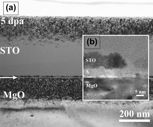
For the (100) domains, the interface assists in the annihilation of irradiation-induced defects such that defect recovery is faster than defect production. In this case, the region near the interface does not amorphize. This is supported by a separate series of experiments in which a purely [100] oriented film was grown on (100) MgO and irradiated to peak doses of 5 dpa. As shown in Figs. 8(a) and 8(b), the STO near the interface remains crystalline even to this higher dose by which the rest of the film is almost amorphized. Interestingly, as shown in the inset, there is a very thin layer of amorphous STO just at the interface, between the crystalline STO and the MgO substrate. Thus, the final morphology of the irradiated film is very complex: the MgO substrate, a very thin (1–2 nm) layer of amorphous STO, an effective defect denuded zone in which the STO is crystalline, and finally amorphous STO. This is reminiscent of the behavior seen at grain boundaries in irradiated Cu, where there is both a denuded zone of voids near the boundaries but an enhanced concentration of voids at the boundaries themselves, indicating a spike in defect content at the boundary.Reference Han, Demkowicz, Fu, Wang and Misra44 Similar defect profiles, showing a denuded zone near an interface containing large concentrations of defects, have been predicted near model interfaces. The amorphous layer we observe at the interface could have a similar origin. This complex morphology demonstrates the complicated response of these materials to damage processes.
(a) Irradiated STO/MgO to 5 dpa using light neon irradiation. (b) High resolution micrograph at the interface of STO/MgO showing the presence of a crystalline denuded zone surrounded by an amorphous STO.
In contrast, for the (110) domains, the damage initially leads quickly to amorphization, for reasons discussed above. However, once the STO in these domains has been amorphized, it begins to recrystallize, assisted or seeded by the crystalline (100) domains nearby and the faster annihilation rate of defects near the STO/MgO interface. This explanation is consistent with experiments by Meldrum et al.Reference Meldrum, Boatner, Weber and Ewing45 who observed recrystallization of STO, amorphized via ion beams, when exposed to electron beams. In that case, the production rate is much higher in the case of ion beams than electron beams. As the relative annihilation rate/production rate increases because of the weaker damage production induced by electrons, the material is able to recover, again assisted by the nearby crystalline regions. In our case, the differences in relative annihilation rate/production rate are not a consequence of differing irradiation conditions, but by structural differences in different regions of the film.
The processes schematically illustrated in Figs. 6 and 7 represent a physical model that is consistent with the experimental observations presented here and in the literature. We recognize that many details are missing, in particular relating to how defect annihilation is enhanced at the interface and the precise sequence of steps by which the final irradiated morphology is reached. These details are the subject of ongoing work.
C. Other considerations
Another factor that could play a role in the different rates of damage accumulation in the (100) versus (110) domains is the fact that these have differing orientations with respect to the ion beam and could, in principle, experience different base rates of defect production. Indeed, experiments by Usov et al.Reference Usov, Arendt, Groves, Stan and DePaula46 on MgO and YSZ found that differently oriented single crystals exhibited different rates of damage accumulation. However, in irradiation experiments of polycrystalline STO, researchersReference Uberuaga and Bai47 found very little difference in the damage response of the different domains after irradiation with 10 MeV Au. This suggests that if there is a dependence on damage accumulation with respect to orientation, it is rather weak and is not sufficient to cause such great changes in amorphization susceptibility. Yet this is not a direct proof that channeling effects are unimportant since the domains in the polycrystalline experiment were randomly oriented and do not necessarily match the orientations in our films. Their results are however consistent with ours if we consider the amorphization appears to initiate at the STO/MgO interface and progress from there throughout the remainder of the film. If orientation and channeling were important factors we would expect the domains to amorphize more uniformly. Based on these considerations, we speculate that channeling is not the reason for the early onset of amorphization, as given in our previous experiments,Reference Won, Vernon, Karakuscu, Dickerson, Cologna, Raj, Wang, Yoo, Lee, Misra and Uberuaga32,Reference Karakuscu, Cologna, Yarotski, Won, Francis, Raj and Uberuaga48 but rather the enhanced amorphization of the (110) domains is a direct consequence of the STO/MgO interfacial properties.
Regarding the incorporation of Ti into the MgO substrate [Fig. 5(d)], we suspect that this is a purely ballistic effect associated with the irradiation. We performed the same materials characterization on the virgin thin films and did not see any intermixing into the substrate layer below associated with the deposition. This behavior is therefore consistent with molecular dynamics simulations of collision cascades at the HfO2/MgO interface by Valone et al.Reference Valone, Uberuaga, Liu, Jeon, Chaudhry and Grønbech-Jensen49 In that case, on the time scale of the collision cascade, Hf ballistically mixed into the MgO and remained trapped as interstitial species. Hf is arguably similar to Ti; both are transition-metals with similar valence structure, ionic radii, and studies have shown similar incorporation behavior into alloysReference Firstov, Van Humbeeck and Koval50 and ceramics.Reference Afanas’ev, Stesmans, Chen, Li and Campbell51 It seems reasonable to conclude that Ti behaves similarly in our films and the timescale for Ti to diffuse out of MgO is significant at room temperature. We speculate that if the experiments were conducted at an elevated temperature, either the Ti would be able to diffuse back to the interface or, perhaps, the kinetics would allow for the formation of a Mg–Ti–O reaction phase at the interface, induced by irradiation damage.
As has been observed by numerous researchers,Reference Oyoshi, Hishita and Haneda19–Reference Zhang, Lian, Wang, Jiang, Ewing and Weber21 the amorphization behavior of STO is very sensitive to the electronic aspects of the irradiation. Not only does changing the amount of electronic energy deposition significantly influences the rate of amorphization,Reference Oyoshi, Hishita and Haneda19 but electron beams can recrystallize amorphous STO.Reference Nakao, Wang, Jin, Miyagawa and Miyagawa20 However, we do not believe that the behavior we report here is dominated by electronic effects. First, single domain (100) STO, irradiated and characterized with the same conditions as used here, did not experience recrystallization under the TEM (Fig. 8). Further, the most important phenomenon, the enhanced amorphization of the (110) domains, seems to be connected to the interface properties of the material. It is possible that the recrystallization at the interface is related to local electronic effects, though it may also be enhanced defect recombination induced by the interface.
It is interesting to speculate on other implications of our findings. After irradiation to a relatively moderate dose, the film has attained a two-phase structure, with crystalline (100) domains and amorphous (110) domains. Such two-phase amorphous/crystalline materials have been studied for their exceptional hardness.Reference Vepek52 Thus, ion beam implantation may be a tool for patterning and modifying thin films for functional applications.
A final important point is that, as mentioned above, in all of our previous irradiations of STO-bearing oxide bilayers,Reference Zhuo, Uberuaga, Yan, Fu, Dickerson, Wang, Misra, Nastasi and Jia23,Reference Bi, Uberuaga, Vernon, Fu, Wang, Li, Wang, Misra and Jia24,Reference Zhuo, Fu, Yan, Wang, Zhang, Dickerson, Uberuaga, Misra, Nastasi and Jia53 we typically observed that the STO at the interface was either damaged more easily than far-away in the matrix or not significantly influenced by the interface. In no prior case did we observe enhanced radiation tolerance on the STO side of the interface. We attributed this behavior to the relative thermodynamics and kinetics of defects in the two phases comprising the bilayer based on a reaction-diffusion model. The model suggested defect build-up at precisely the interface because it impeded defect flow into the preferred phase.Reference Uberuaga, Martinez, Bi, Zhuo, Jia, Nastasi, Misra and Caro25 The main conclusion from those studies was that the response of one material in a nanocomposite to irradiation was very sensitive to the nature of the other materials present within the composite. In the present case, we find that the STO exhibits a crystalline denuded zone at the interface – that the interface significantly accelerates the annihilation of defects on the STO side of the interface. Overall this supports our previous suggestion that the radiation tolerance of one component can be significantly influenced by the pairing with other materials.Reference Uberuaga, Martinez, Bi, Zhuo, Jia, Nastasi, Misra and Caro25
V. CONCLUSIONS
A systematic experimental investigation of the structural and chemical evolution before and after irradiation at the STO/MgO interface was performed. The goal was to understand the structure–property–chemistry relationship between orientation and phase stability under irradiation.
Our results demonstrate that the model bilayer exhibits differences in radiation tolerance based on the local orientation of the STO/MgO interface. Detailed analytical characterization enabled us to profile thin films following irradiation, accounting for changes in both structure and chemistry. We find that STO (110) domains amorphize more readily than STO (100) domains when both are grown on the same MgO (100) substrate. We attribute this difference to differences in the electrostatic structure of the two domains relative to the (100) MgO substrate. In particular, we suggest that radiation-induced defects at the interface form a space charge layer that interacts and destabilizes the charged planes of (110) STO, but do not significantly interact with the (100) domains.
The second important observation is that a persistent crystalline layer of STO (100) forms near the interface even after the majority of the film has amorphized. Further, regions of (110) STO domains that initially amorphized are observed to recrystallize. This is a consequence of enhanced annihilation at the interface, which sustains the crystallinity of the (100) domains and aids in the recrystallization of the amorphized (110) domains, a recrystallization which is effectively seeded by the (100) domains. This is a unique finding for STO which, in all other cases previously examined, exhibited reduced radiation tolerance at heterointerfaces.Reference Uberuaga, Martinez, Bi, Zhuo, Jia, Nastasi, Misra and Caro25
In conclusion, our results further support the concept that the radiation tolerance of the component phases of a composite is very sensitive to the nature of the other phases present.Reference Uberuaga, Martinez, Bi, Zhuo, Jia, Nastasi, Misra and Caro25 In addition, they indicate that the interfacial structure, both structurally and chemically, is an important factor in the radiation response of the material. Together, these observations provide new insight into the performance and ultimately the design of oxides for advanced technical applications.
ACKNOWLEDGMENTS
This work was supported by the Center for Materials at Irradiation and Mechanical Extremes (CMIME), an Energy Frontier Research Center (EFRC) funded by the U.S. Department of Energy, Office of Science, Office of Basic Energy Sciences under Award Number 2008LANL1026. The work was performed, in part, at the Center for Integrated Nanotechnologies, an Office of Science User Facility operated for the U.S. Department of Energy (DOE) Office of Science. We acknowledge Dorothy Coffey at ORNL for fabricating our FIB foils and Yun Xu for depositing our films. JAA acknowledges access to the ORNL's ShaRE User Facility, which is sponsored by the Scientific User Facilities Division, Office of Basic Energy Sciences, U.S. Department of Energy, where part of the TEM work was performed in collaboration with Miaofang Chi and the LeRoy Eyring Center for Solid State Science at ASU, where part of the TEM work was performed in collaboration with Toshihiro Aoki and Jiangtao Zhu. We also acknowledge helpful discussions and editorial support from Terence Mitchell, Maulik Patel, and Michelle Hanenburg.