Introduction
Plasmonic waveguides[ Reference Takahara and Kobayashi 1 , Reference Brongersma, Schuller, White, Jun, Bozhevolnyi, Sondergaard, Zia and Bozhevolnyi 2 ] are metallic optical waveguides that can transport optical information as surface plasmon polaritons (SPPs),[ Reference Barnes, Dereux and Ebbesen 3 – Reference Miyata and Takahara 5 ] which are electromagnetic waves coupled to free electron oscillations on a metal surface. As they are capable of confining guided plasmon modes into smaller volumes beyond the diffraction limit at optical frequencies, plasmonic waveguides have recently attracted interest for use as subwavelength optical waveguides in nanoscale optical circuits. To transmit SPPs, various types of plasmonic waveguides, such as cylindrical metal nanorods,[ Reference Takahara, Yamagishi, Taki, Morimoto and Kobayashi 6 ] slab waveguides,[ Reference Berini 7 ] slot waveguides,[ Reference Veronis and Fan 8 ] and metal grooves,[ Reference Pile and Gramotnev 9 ] have been proposed. In recent years, crossing plasmonic waveguides[ Reference Xiao and Mortensen 10 – Reference Ota, Fukuhara, Sumimura, Ito, Aihara, Ishii and Fukuda 12 ] have been suggested for integrated optical components. These structures are composed of several physically connected waveguides placed on a substrate. Compared with bypass wiring without crossing, crossing waveguides make it possible to connect optical devices at shorter distances. This capability leads to decreases in total propagation losses during information transmission. In addition, owing to increases in wiring densities per unit area, these structures are key elements in realizing high-density optical networks and intricately patterned photonic devices. Ideally, an optical signal on a crossing waveguide should be fully transmitted forward through their intersections. Unfortunately, due to scattering at the crossing points, propagating light experiences undesirable energy dissipation such as by radiation to the surroundings, reflection, and energy escaping to sideways (crosstalk), leading to degradation of the signal transmission performance.[ Reference Manolatou, Johnson, Fan, Villeneuve, Haus and Joannopoulos 13 , Reference Fukazawa, Hirano, Ohno and Baba 14 ] Such energy dissipation would be further pronounced in waveguide structures with imperfections. Although various structures of plasmonic crossing waveguides based on resonant tunneling,[ Reference Xiao and Mortensen 10 ] multimode interference (MMI),[ Reference Li, Xu, Zeng, Wang, Yang, Yu and Jiang 11 ] or mirror-imaged MMI,[ Reference Ota, Fukuhara, Sumimura, Ito, Aihara, Ishii and Fukuda 12 ] have been reported as potential solutions, it is still challenging to completely suppress the impact of scattering at the crossing points because the crossing waveguides in these structures are physically connected.
Here we experimentally demonstrate surface plasmon propagation on an overcrossing metallic waveguide (nanobridge). The nanobridge is fabricated by a modified version of a previously developed pick-and-place method.[ Reference Lindquist, Johnson, Norris and Oh 15 , Reference Miyata, Holsteen, Nagasaki, Brongersma and Takahara 16 ] By spatially separating the two waveguides, the energy dissipation at the crossing point can be greatly suppressed because SPPs can propagate across the waveguides without experiencing the scattering. In addition, we numerically demonstrate the crossing-angle-independent operation of SPP transmission. Our approach based on the overcrossing waveguides would potentially lead to the development of high-density integration of optical waveguides.
Fabrication methods and optical setup
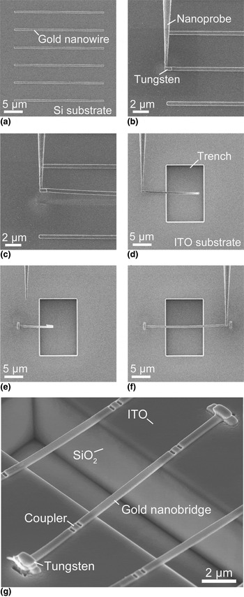
Figures 1(a)–1(f) show scanning ion microscope images of the steps in the nanobridge fabrication procedure based on the pick-and-place method. First, patterned gold nanowires (NWs) with widths of 500 nm and thicknesses of 150 nm are fabricated on a silicon substrate by the electron beam lithography and vacuum deposition system [Fig. 1(a)]. Next, a three-dimensionally manipulated tungsten nanoprobe is brought near one end of the NW. After welding the nanoprobe to the NW using focused ion beam-induced tungsten deposition [Fig. 1(b)], the NW is lifted up from the silicon substrate by manipulating the nanoprobe [Fig. 1(c)]. The lifted NW is moved onto a trench fabricated by focused ion beam (FIB) milling on an indium tin oxide (ITO)-coated SiO2 substrate [Fig. 1(d)]. The ITO layer is used to prevent charging of the SiO2 substrate during the ion beam exposure. This layer is also needed to reduce back scattering of incident light from the substrate during measurements. Then, one side of the NW is placed across the trench and welded to the substrate by tungsten deposition [Fig. 1(e)]. After welding, the nanoprobe is cut from the NW using FIB milling. Finally, the NW is wired over a trench by the nanoprobe and the other side of the NW is welded to the substrate by tungsten deposition [Fig. 1(f)]. Figure 1(g) shows an oblique scanning electron microscope (SEM) image of the fabricated gold nanobridges which cross over a trench with a width of 5 µm and a depth of 6 µm. Both ends of the nanobridge are fixed onto the substrate with tungsten. Each slit near the end of the nanobridge is an input/output coupler. For SPP excitation, the couplers are numerically optimized to efficiently couple incident light (wavelength λ 0 = 635 nm) to SPPs on the nanobridge.
Pick-and-place method. (a) Gold NWs with widths of 500 nm and thicknesses of 150 nm on a silicon substrate. (b,c) Picking up the NW from the substrate by a tungsten nanoprobe. (d–f) Wiring the NW over a trench. The lifted NW is moved to the trench on an ITO-coated SiO2 substrate, and ends of the NW are fixed onto the substrate to form a bridge across the trench. (g) Oblique SEM image of fabricated nanobridges. The trench is 5 µm wide and 6 µm deep.

To demonstrate surface plasmon propagation on the fabricated nanobridge, a linear polarized laser beam (λ 0 = 635 nm) was focused through an objective lens (100×, NA = 0.9) onto a coupler on the fabricated nanostructure. Signals from the output coupler were detected by a charge-coupled device camera. To reduce scattering of incident beam from the input coupler, cross-polarization detection[ Reference Wen, Banzer, Kriesch, Ploss, Schmauss and Peschel 17 ] was used.
Results and discussions
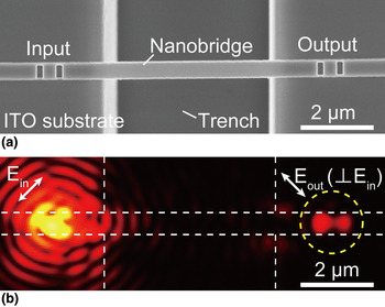
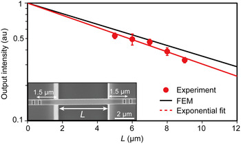
We start by investigating propagation properties of SPPs on straight nanobridges. Figure 2(a) shows an SEM image of a straight gold nanobridge crossing over the trench. When the laser beam is irradiated on the input coupler, strong scattering from the output coupler is observed as shown in Fig. 2(b). This result clearly indicates that SPPs are efficiently excited and propagate on the nanobridge. To quantify propagation properties of the excited SPPs, the propagation length L p of SPPs is experimentally obtained. Figure 3 shows the experimentally observed output intensity as a function of the length L of the suspended part of the nanobridge (shown in the inset of Fig. 3). The length from the coupler to the edge of the trench is fixed at 1.5 µm. The black solid line shows calculated values using a finite element method. The geometrical parameters of the gold waveguide surrounded by air are same as the measured value of the nanobridge. In all calculations, relative permittivity of gold is obtained from experimental data.[ Reference Johnson and Christy 18 ] The red solid circles represent experimentally obtained values, and the red dotted line is an exponential fit of the experimental values. From the experimental results in Fig. 3, a value of L p = 8.4 µm is obtained, which is in agreement with the FEM calculations (L p = 9.6 µm). This slight deviation between the numerical and experimental propagation lengths may be attributed to the distortion of the nanobridges and the structural imperfection. These results confirm that the suspended waveguide is capable of transmitting SPPs between two distant points over the trench.
Surface plasmon propagation on a straight nanobridge. (a) SEM image of the nanobridge. Each slit near the edge of the trench is an input/output coupler. (b) Experimentally observed scattering from the output shown by a yellow dashed circle. The polarization direction of the incident beam and the transmission axis of the output polarizer are indicated by the white arrows. The axis of the output polarizer is perpendicular to the incident beam polarization.

Output intensity versus waveguide length L. The black solid line shows calculated values using a FEM. The red solid circles represent experimentally obtained values, and the red dotted line is an exponential fit of the experimental values. A propagation length L p = 8.4 µm is experimentally obtained. The inset shows an SEM image of the nanobridge. The length from the coupler to the edge of the trench is 1.5 µm.

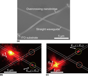
In the next step, we demonstrate surface plasmon propagation on an overcrossing nanobridge fabricated by the pick-and-place method. Figure 4(a) shows an oblique SEM image of a nanobridge crossing over a straight waveguide placed on an ITO substrate. The two waveguides are spatially separated. The gap distance between the two waveguides is about 1.3 µm, and the crossing angle is 60°. When the laser beam is irradiated on the input coupler on either the straight waveguide [Fig. 4(b)] or the overcrossing nanobridge [Fig. 4(c)], strong scattering is observed from the corresponding output (yellow circle). It is important to note that no output signal from the other output coupler shown by the red circle is observed. This result means that SPPs can propagate on either waveguide without any interaction with the other waveguide.
Surface plasmon propagation on an overcrossing nanobridge. (a) Oblique SEM image of a fabricated nanobridge crossing over a straight waveguide placed on an ITO substrate. These waveguides are 500 nm wide and 150 nm thick. The gap distance between the two waveguides is about 1.3 µm, and the crossing angle is 60°. (b, c) Experimentally observed scattering from the outputs shown by yellow dashed circles. Scattering is not observed at the other output couplers shown by red solid circles. The white arrows depict the polarization direction of the incident beam and the transmission axis of the output polarizer. The axis of the output polarizer is orthogonal to the incident beam polarization.

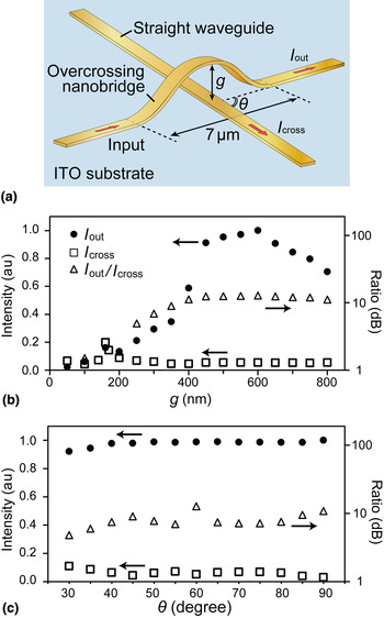
To further investigate the character of the overcrossing waveguide, we numerically analyze the gap distance dependence of the output intensity and the crosstalk intensity. For these calculations, finite-difference time-domain simulations by using a commercial solver (Synopsys FullWAVE) were performed. Figure 5(a) shows a schematic view of a calculation model of the overcrossing nanobridge. Relative permittivity of SiO2 is obtained from experimental data.[ Reference Palik 19 ] The refractive index of the ITO was found to be 1.86 + i0.029 from an ellipsometry measurement. The length of the suspended part is fixed at 7 µm. The crossing angle θ is fixed at 60°. Figure 5(b) shows the dependence of the output intensity I out through the overcrossing nanobridge and the crosstalk intensity I cross through the straight waveguide as a function of the gap distance g between the two waveguides. I cross means output intensity from the waveguide, which is not irradiated with the laser beam. The filled circles and the open squares correspond to I out and I cross, respectively. These intensities are normalized to the maximum value of I out. The open triangles correspond to the ratio I out/I cross with dB. In Fig. 5(b), I out rapidly increases as g increases, then reaches a maximum at g = 600 nm. This trend is ascribed to the fact that undesirable energy dissipation, such as by radiation to surroundings and reflection from the intersection, is suppressed by moving the suspended part of the nanobridge away from the straight waveguide. This energy dissipation will arises from a spatial overlap between the electric fields of the guided plasmon modes and the straight waveguide. The penetration depth[ Reference Barnes 20 ] d of the electric field to the air is represented by
 $$d = \displaystyle{{{{\lambda} _0}} \over {2\pi}} \sqrt { - {\varepsilon _m} - 1},$$
where ɛ m is the relative permittivity of the metal. In this case, d is about 340 nm at λ 0 = 635 nm. This value is in agreement with the gap distance from which I out begins to rapidly increase. This indicates that the energy dissipation can be suppressed by separating the two waveguides beyond the penetration depth. After reaching the peak, I out gradually decreases. This can be understood by increases in the propagation and bending losses. In the general case of lossy waveguides, the output intensity drops as the length of the waveguide is extended. Moreover, the radius of curvature of the overcrossing nanobridge decreases as g increases. Therefore, the intensity also drops due to bending losses. These factors can potentially lead to the gradual decrease in I out as g increases. In contrast, the crosstalk intensities for almost all gap sizes are less than the corresponding output intensities. This lower I cross implies that coupling to the guided modes on the straight waveguide is weak even though the gap distance is small. These results reveal that by adjusting the gap distance to an optimum value, the energy dissipation can be suppressed while achieving high I out.
Propagation properties of the overcrossing nanobridge. (a) Schematic view of a calculation model of the overcrossing nanobridge. The length of the suspended part is fixed at 7 µm. (b) Output intensity I out through the overcrossing nanobridge and crosstalk intensity I cross through the straight waveguide as a function of the gap distance g between the two waveguides. The filled circles and the open squares correspond to I out and I cross, respectively. The open triangles correspond to the ratio I out/I cross with dB. These intensities are normalized to the maximum value of I out. The crossing angle θ is fixed at 60°. (c) I out and I cross as a function of crossing angle θ. The gap distance is fixed at 600 nm.

We also investigate the crossing angle dependence of I out and I cross. Here, the gap distance is fixed at 600 nm. Figure 5(c) shows I out and I cross as functions of the crossing angle θ. For θ < 30°, propagating SPPs couples to the adjacent waveguide before SPPs enter to the overcrossing part. Therefore, the crossing angle is defined as 30° ≤ θ ≤ 90°. As shown in Fig. 5(c), intensity does not depend greatly on the crossing angle. In addition, I out is obviously higher than I cross at any angle. These results suggest that SPP transmission based on the overcrossing waveguide is independent of the crossing angle. The nanobridge structure is thus capable of SPP transmission crossing over another waveguide at any angle without undesired interaction.
Conclusion
We experimentally demonstrated surface plasmon propagation on an overcrossing nanobridge. The spatially separated crossing waveguide was able to be fabricated by employing the pick-and-place method. Our measurements showed that SPPs can cross over another waveguide without any interaction. Furthermore, through numerical analysis, we showed that the overcrossing nanobridge enables SPPs to cross over another waveguide while suppressing energy dissipation by separating the two waveguides beyond the field penetration depth of the guided plasmon modes. An angle-independent crossing waveguide can be also designed by selecting the optimum gap distance between the two waveguides. We believe that our approach might be “a new pathway” for high-density integration of optical waveguides.
Acknowledgments
This work was supported by Grant-in-Aid for Scientific Research B (no. 25286007) from the Ministry of Education, Culture, Sports, Science and Technology, Japan (MEXT). M. M. is supported by Research Fellowships of Japan Society for the Promotion of Science (JSPS) for Young Scientists. Y. N. is supported by Interactive Materials Science Cadet Program of Osaka University.