
I. INTRODUCTION
The conversion of light into electrical signal had tremendous applied potentials in many technologies which can affect our daily lives such as optical communication, vision, medical imaging, light-emitting diodes, remote sensing, and gas sensor. Reference Xue, Zhang, Liu, Liu, Song, Sophia, Liu, Xu, Xu, Wang, Zheng, Liu, Li and Bao1–Reference Yu, Liu, Gan, Hu, Zhang, Li, Kang, Terrones and Lv3 Extensive studies had been done to explore secrets of the interaction between light and materials, which lead to the finding of many interesting and revolutionary scientific fundamental phenomena. Reference Butun, Palacios, Cain, Liu, Dravid and Aydin4,Reference Saran and Curry5 The interaction between light and materials was at the heart of optoelectronic systems that required detection of light. Detection of light can be achieved by the photoabsorber material in photodetectors which can convert incident photons into electrical signals. Reference Mehew, Unal, Torres Alonso, Jones, Fadhil Ramadhan, Craciun and Russo6 Two-dimensional (2D) materials including graphene and transition metal dichalcogenides (TMDCs) have been widely investigated as photoabsorber material in photodetectors due to their unique optical characteristics and mechanical flexibility that enable the development of wearable electronic devices. Reference Mehew, Unal, Torres Alonso, Jones, Fadhil Ramadhan, Craciun and Russo6,Reference Buscema, Groenendijk, Blanter, Steele, van der Zant and Castellanos-Gomez7 Graphene was firstly discovered as a 2D material and an appealing material for photodetectors. Reference Mueller, Xia and Avouris8,Reference Jabbarzadeh, Siahsar, Dolatyari, Rostami and Rostami9 Photodetectors based on graphene have been widely investigated over the past few years and shown to exhibit exceptionally high carrier mobility [106 cm2/(V s) at 2 K and 105 cm2/(V s) at room temperature], Reference Knap, Deng, Rumyantsev and Shur10,Reference Bolotin, Sikes, Jiang, Klima, Fudenberg, Hone, Kim and Stormer11 excellent chemical stability, Reference Drieschner, Weber, Wohlketzetter, Vieten, Makrygiannis, Blaschke, Morandi, Colombo, Bonaccorso and Garrido12,Reference Li, Niu, Zheng and Yan13 high mechanical strength, Reference Mortazavi14,Reference Wang, Williams, Boutilier, Kidambi and Karnik15 and particular broadband spectral response from visible to far infrared. Reference Li, Niu, Zheng and Yan13,Reference Koppens, Mueller, Avouris, Ferrari, Vitiello and Polini16 However, the difficulty in opening up the band gap of graphene resulted in a high dark current which greatly limited its application in photodetection. Reference Yu, Li, Zhang, Ma, Sun, Yuan, Fu and Bao17 However, layer-structured TMDCs such as MoS2, Reference Lopez-Sanchez, Lembke, Kayci, Radenovic and Kis18 tungsten disulfide (WS2), Reference Cui, Xin, Yu, Pan, Ong, Wei, Wang, Nan, Ni, Wu, Chen, Shi, Wang, Zhang, Zhang and Wang19 SnS, Reference Ahn, Lee, Heo, Sung, Kim, Hwang and Jo20 and InSe Reference Yang, Jie, Mak, Lin, Lin, Yang, Yan, Lau and Hao21 possess a finite band gap that can be widely tuned by layer number and strain, high carrier mobility, strong light–matter interaction, and complementary metal–oxide–semiconductor transistor-compatible fabrication routines, Reference Cao, Liu and Banerjee22–Reference Island, Kuc, Diependaal, Bratschitsch, van der Zant, Heine and Castellanos-Gomez24 which enable the development of photodetectors with multifunction, low power consumption, and high performance that are required for the next generation optoelectronics.
However, photodetectors with high responsivity, spectrally broadband, and high detectivity are currently extremely difficult to realize in a single TMDC because of their thickness-limited light absorption and band-gap–limited spectral range. Reference Wang, Kalantar-Zadeh, Kis, Coleman and Strano25 Building photodetectors composed of TMDCs with other light sensitizing materials of different band gaps was an efficient route to realize high-performance light detection. Reference Kagan, Lifshitz, Sargent and Talapin26,Reference Lan, Li, Wang, Yin, Guo, Liu and Liu27 On one hand, the sensitizer with high absorptivity can improve the light absorption efficiency of the photodetector device on the basis of TMDCs. Reference Rauch, Böberl, Tedde, Fürst, Kovalenko, Hesser, Lemmer, Heiss and Hayden28–Reference Kufer, Nikitskiy, Lasanta, Navickaite, Koppens and Konstantatos30 However, the sensitizer layer has to be thin enough to retain excellent merits of 2D materials. On the other hand, candidates for sensitizing materials can vary from metals, semimetals, semiconductors, to insulators, which offer great opportunity to develop hybrid photodetector with response in a wide spectral range. Reference Jia, Xiang, Wen, Yang, Hao and Liu31,Reference Xu, Lin, Li, Zhang, Wu, Xu, Lu and Xu32 In addition, sensitizer can be chosen with high carrier mobility and appropriate band structure that aligns well with TMDCs, so that the charge can be efficiently separated and transferred at the interface which facilitates the high responsivity and response speed. Recently, using colloidal quantum dots (CQDs) and nanosheets (NSs) of different band gaps as the sensitizer, ultrasensitive, fast, and broadband photodetectors have been realized due to the synergetic effect of the strong absorption of the sensitizer and the extremely fast circulation of the carrier within 2D TMDCs. Reference Yu, Zhang, Song, Zhang, Cao, Che, Dai, Yang, Zhang and Yao29,Reference Jia, Xiang, Wen, Yang, Hao and Liu31,Reference Jia, Li, Xiang, Wen, Bao, Feng, Yang and Liu33
In this article, we review the photodetection performance of recent progress on hybrid photodetectors based on 2D TMDCs with sensitizing materials such as zero-dimensional quantum dots (QDs)s, one-dimensional nanotubes or nanowires, and 2D NSs. Firstly, the optical properties of TMDCs and physical mechanisms of photodetectors based on TMDCs are introduced. Then we discuss the figure-of-merits of photodetectors based on TMDCs manipulated with various kinds of experiment techniques. In the end, we give a short outlook on the possible routes toward developing high-performance photodetector.
II. OPTICAL AND TRANSPORT PROPERTIES OF TMDCS
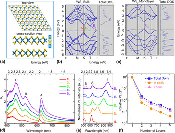
TMDC materials consist of a transition metal element M (such as Mo, W, and Ti) and a chalcogen X (S, Se, or Te). Monolayer of TMDCs such as WS2 contained an X–M–X sandwich structure as shown in Fig. 1(a). 2D TMDC materials are stacked via the van der Waals interaction between layers. The electronic band structure of TMDCs plays a key role in absorbing or emitting light and directly influences their optical properties. Figures 1(b) and 1(c) show a typical electronic band structure calculated via the first principle quantum codes for WS2 in different thicknesses. Reference Gutiérrez, Perea-López, Elías, Berkdemir, Wang, Lv, López-Urías, Crespi, Terrones and Terrones34 A strong dependence of the electronic structure on the layer number is demonstrated. For bulk WS2, the band gap is 1.3 eV with an electronic indirect transition which originated from hybridization between tungsten d-orbitals and sulfur p z -orbitals. Reference Wang, Kalantar-Zadeh, Kis, Coleman and Strano25 The splitting of the valence band is evident at K point in the first Brillouin zone due to the strong spin–orbital coupling and is verified by the absorption measurements. Reference Frey, Tenne, Matthews, Dresselhaus and Dresselhaus35 Upon decreasing the layer number, the band gap is increased, reaching a value of 2.3 eV in monolayer. The electronic transition changes from indirect to direct and the disappearance of band splitting result in one single and strong emission peak in the photoluminescence (PL) spectra. Reference Gutiérrez, Perea-López, Elías, Berkdemir, Wang, Lv, López-Urías, Crespi, Terrones and Terrones34,Reference Xu, Yao, Xiao and Heinz36 The optical band-gap energy determined for monolayer WS2 is 2.05 eV, which is much smaller than the calculated one owing to the large binding energy of excitons. Similar physical phenomena are observed in other TMDCs such as WSe2, MoS2, and MoSe2. Reference Wang, Gong, Shi, Chow, Keyshar, Ye, Vajtai, Lou, Liu and Ringe37,Reference Hu, Dong, Yang, Qiao, Yang, Deng, Yuan, Khan, Lan, Song and Tang38
(a) Top and cross-section view of WS2 atomic structure. Electronic band structure (left) and total density of states (DOC; right) for (b) bulk and (c) monolayer WS2, respectively; Reference Gutiérrez, Perea-López, Elías, Berkdemir, Wang, Lv, López-Urías, Crespi, Terrones and Terrones34 (d) differential reflectance spectra; (e) normalized PL spectra with different layer numbers; and (f) relative quantum yield of mechanically exfoliated WS2 as function of layer number. Reference Zhao, Ghorannevis, Chu, Toh, Kloc, Tan and Eda39 (Reprinted with permissions from: (a–c) Gutiérrez et al., Reference Gutiérrez, Perea-López, Elías, Berkdemir, Wang, Lv, López-Urías, Crespi, Terrones and Terrones34 and (d–f) Xu et al., Reference Zhao, Ghorannevis, Chu, Toh, Kloc, Tan and Eda39 © 2013, 2014 American Chemical Society, respectively.)

Most monolayer TMDCs are optically transparent, where the transmission is over 85%, and have absorption of 5–10% for light in the visible regime. Reference Li, Chernikov, Zhang, Rigosi, Hill, van der Zande, Chenet, Shih, Hone and Heinz40,Reference Bernardi, Palummo and Grossman41 The absorption efficiency is slightly smaller than Si of a comparable thickness. With the increase of thickness, both the reflectivity and absorption increases greatly and become opaque at thicknesses approximately over 5 layers WS2. Reference Chernikov, Berkelbach, Hill, Rigosi, Li, Aslan, Reichman, Hybertsen and Heinz42 There are also fine structures in the differential reflectance spectra, three excitonic absorption peaks in Fig. 1(d) located at 625 nm (peak A), 550 nm (peak B), and 460 nm (peak C). The first two peaks arise from the direct band-gap transitions for WS2, Reference Zhao, Ghorannevis, Chu, Toh, Kloc, Tan and Eda39,Reference Bromley, Knights and Liang43 and the last one is due to the optical transitions between the valence and conduction bands. Reference Yang, Wilkinson, Austin and O’Donnell44 These characteristic peaks display a redshift with the increase of thickness. The energy difference between peak A and B commonly defining the strength of spin-orbit interaction is approximately 400 meV for monolayer WS2 consistent with calculated results and impendence of layer number. Reference Zhao, Ghorannevis, Chu, Toh, Kloc, Tan and Eda39,Reference Ramasubramaniam45 The energy differences are dominated by the metal ions, and are about 145–224 meV for MoX2 and ∼410–466 meV for WX2, where X = S and Se, demonstrate a stronger spin–orbital coupling in WX2 due to the larger orbital magnetic moment of W atoms. Reference Zhao, Ghorannevis, Chu, Toh, Kloc, Tan and Eda39,Reference Bromley, Knights and Liang43,Reference Bromley, Murray and Yoffe46
In contrast to absorption, the light emission is highly correlated with thickness of TMDCs. Figure 1(e) shows the PL of WS2 as an example. For monolayer WS2, the emission peak at ∼630 nm (peak A) originates from the direct recombination of electrons at the bottom of conduction band and the holes at the top of the valence band. The intensity of peak A is greatly reduced (by several orders of magnitude) in the bilayer or multilayer due the appearance of indirect transition (peak I) and the decreased recombination time. Reference He, Sheng, Rong, Lee, Li and Warner47,Reference Kim, Kim, Lee, Lee, Choi, Lee, Lee, Jhang, Park, Cheong, Lee and Chung48 Therefore the PL quantum yield is significantly suppressed [Fig. 1(f)]. Reference Zhao, Ghorannevis, Chu, Toh, Kloc, Tan and Eda39 The energy of indirect transition (peak I) is popped up in the bilayer and shifts remarkably toward the lower value upon increasing the thickness. Similar phenomena are observed in other TMDCs. Reference Zhao, Ghorannevis, Chu, Toh, Kloc, Tan and Eda39,Reference He, Sheng, Rong, Lee, Li and Warner47 The band structure of 2D TMDCs can be effectively tailored by the strain effect. Reference Wang, Cong, Yang, Shang, Peimyoo, Chen, Kang, Wang, Huang and Yu49–Reference Dhakal, Roy, Jang, Chen, Yun, Kim, Lee, Kim and Ahn51 In contrast to the other method, the optical and electrical properties can be made possible via strain engineering due to fine and continuous tuning of electronic structure. Reference Wang, Cong, Yang, Shang, Peimyoo, Chen, Kang, Wang, Huang and Yu49,Reference He, Poole, Mak and Shan52 For example, an indirect and a direct band-gap crossover of monolayer TMDCs is induced by a uniaxial tensile strain. Reference Wang, Cong, Yang, Shang, Peimyoo, Chen, Kang, Wang, Huang and Yu49,Reference Rafael, Andrés, Emmanuele and Francisco50,Reference He, Poole, Mak and Shan52 The response of PL spectra to strain in monolayer is different with that in multilayer TMDCs, and significant enhancement of PL intensity is observed in bilayer WSe2 and WS2 due to the transition of the band gap from indirect to direct, Reference Dhakal, Roy, Jang, Chen, Yun, Kim, Lee, Kim and Ahn51,Reference Desai, Seol, Kang, Fang, Battaglia, Kapadia, Ager, Guo and Javey53 however, no change in PL intensity for bilayer MoS2. Reference Conley, Wang, Ziegler, Haglund, Pantelides and Bolotin54 Most of the TMDCs (monolayer and fewer-layer) demonstrate an approximately linear decrease of optical band gap with the increase of tensile strain. Reference Wang, Cong, Yang, Shang, Peimyoo, Chen, Kang, Wang, Huang and Yu49,Reference Dhakal, Roy, Jang, Chen, Yun, Kim, Lee, Kim and Ahn51,Reference Conley, Wang, Ziegler, Haglund, Pantelides and Bolotin54
Electrical transport properties such as carrier mobility are crucial to the performance of 2D TMDC photodetectors. They can be modulated by many factors such as layer thickness, carrier density, effective carrier mass, temperature, and contact resistance. Reference Wang, Kalantar-Zadeh, Kis, Coleman and Strano25,Reference Wei, Yan, Shen, Lv and Wang55,Reference Molina-Sánchez and Wirtz56 The room temperature carrier mobility is calculated to be ∼700 and 400 cm2/V s at the phonon scattering limit for the monolayer of WS2 and MoS2, respectively. Reference Island, Kuc, Diependaal, Bratschitsch, van der Zant, Heine and Castellanos-Gomez24,Reference Chen and Chang57 In practice, the reported carrier mobility of monolayer WS2 and MoS2 is in the range of 0.01–200 cm2/(V s), Reference Huo, Kang, Wei, Li, Li and Wei58–Reference Wang, Wang, Xu, Wang, Wang, Huang, Yin and He60 which is much smaller than that expected by theoretical calculations due to the scattering of carrier originating from dangling bonds on the surface of oxides substrate. By reducing to the scattering effect using a h-BN substrate, a mobility as high as 163 cm2/V s is achieved for monolayer WS2. Reference Iqbal, Iqbal, Khan, Shehzad, Seo, Park, Hwang and Eom61 The carrier mobility of monolayer WS2 field-effect transistors (FETs) on h-BN substrate increases to 408 cm2/V s with the temperature dropping to 5 K. Reference Iqbal, Iqbal, Khan, Shehzad, Seo, Park, Hwang and Eom61 The performance of monolayer MoS2 phototransistor is significantly enhanced due to high carrier mobility of 410 cm2/V s. Reference Molina-Sánchez and Wirtz56
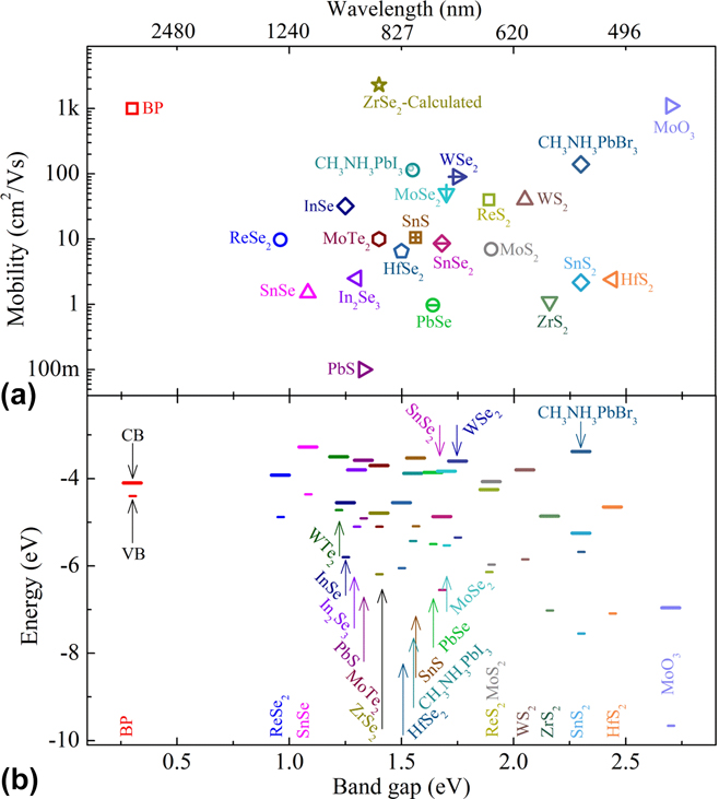
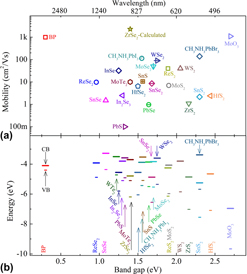
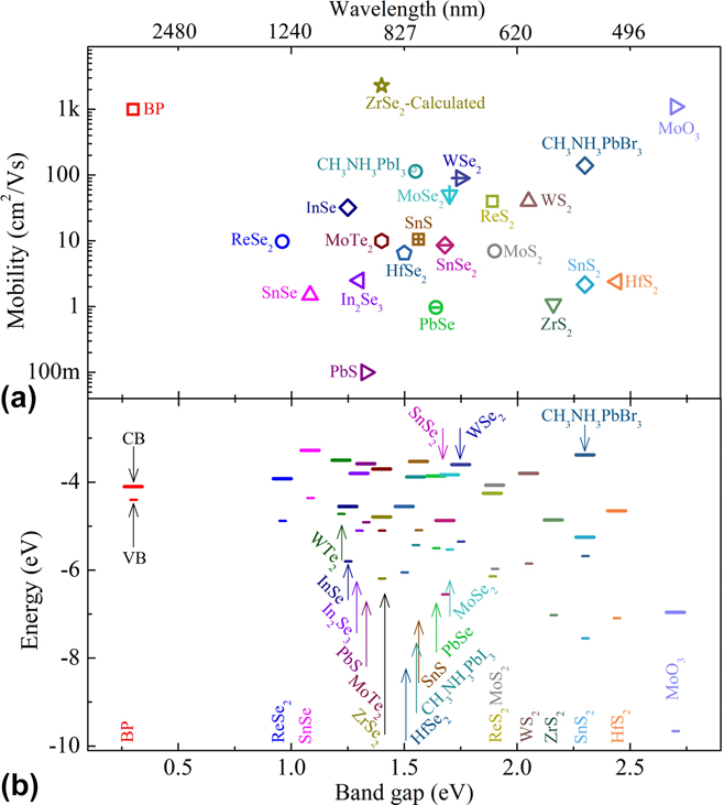
The electrical metal contact to TMDCs is crucial for the replenishment of the photogenerated carrier. The metal/TMDCs tunnel barrier is hard to suppress due to the lack of dangling bonds on the surface of TMDCs, and the Schottky barrier height (SBH) is also difficult to reduce with conventional metal contact due to a strong Fermi-level pinning. Reference Kim, Moon, Lee, Choi, Ahmed, Nam, Cho, Shin, Park and Yoo62 Currently the metal contact becomes a key bottleneck to the development of photodetectors with high performance in terms of responsivity and response speed. Routes such as selective chemical doping of 2D TMDCs and replacement of conventional metals with metallic 2D materials have been demonstrated to be effective in tuning the SBH and achieving good contact, eventually leading to a significant improvement of photodetection performance. Reference Mehew, Unal, Torres Alonso, Jones, Fadhil Ramadhan, Craciun and Russo6,Reference Xu, Cheng, Du, Yang, Yu, Luo, Yin, Li, Dong, Ye and Duan63,Reference Choi, Qu, Lee, Liu, Watanabe, Taniguchi and Yoo64 The contact resistance can be decreased by using graphene as the electrodes while the photodetection performance based on 2D materials has been improved. Reference Luo, Cao, Cai, Feng, Yan, Yan, Zhang and Wang65,Reference Wei, Yan, Lv, Shen and Wang66 The contact resistance has been described in detail in the literature. Reference Buscema, Island, Groenendijk, Blanter, Steele, van der Zant and Castenllanos-Gomez67 The typical band gap and mobility of typical monolayer 2D materials are summarized in Fig. 2.
(a) Mobility and (b) band-gap plot of typical monolayer 2D-materials [except that SnSe (multilayer), InSe (multilayer), HfS2 (7.8 nm), PbS (QDs film), PbSe (NCs film), MoTe2 (fewer-layers), HfSe2 (fewer-layers), SnSe2 (84 nm), MoO3 (8-layer), SnS (not applicable, N/A), SnS2 (N/A), CH3NH3PbI3, and CH3NH3PbBr3 (film)]; all mobilities cited from Refs. Reference Xue, Zhang, Liu, Liu, Song, Sophia, Liu, Xu, Xu, Wang, Zheng, Liu, Li and Bao1, Reference Ahn, Lee, Heo, Sung, Kim, Hwang and Jo20, Reference Wang, Gong, Shi, Chow, Keyshar, Ye, Vajtai, Lou, Liu and Ringe37, and Reference Li, Yu, Ye, Ge, Ou, Wu, Feng, Chen and Zhang68–Reference Xu, Wang, Wang, Huang, Wang, Yin, Jiang and He86. Band alignment of various monolayer 2D-materials [except that SnSe (N/A), SnS (N/A), InSe (Bulk), PbS (QDs film), PbSe (QDs film), CH3NH3PbI3 and CH3NH3PbBr3 (film)]; all the parameters cited from Refs. Reference Li, Wang, Zhang, Zou, Xu and Zhang87–Reference Butler, Crespo-Otero, Buckeridge, Scanlon, Bovill, Lidzey and Walsh97.
III. KEY FIGURES-OF-MERIT AND PHOTODETECTION MECHANISMS OF PHOTODETECTORS
The capability for a photodetector to convert light into electric signal relies primarily on the optical absorption by which extra carriers are generated, the separation efficiency of photogenerated electron–hole pairs driven by a local or external electric field, and operating temperature. Several essential figures-of-merit have to be introduced to evaluate a photodetector and facilitate comparison between photodetectors fabricated with different photosensitive materials and in different geometries. The widely used figures-of-merit for photodetector include responsivity (R), response time (τ), specific detectivity (D*), and spectral selectivity, and high performance photodetectors are considered to have large responsivity, short response time, high specific detectivity, and wide spectral selective range in wavelength.
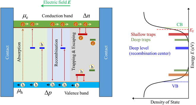
The responsivity R = I ph/P eff measures the variation of electrical output current I ph between illumination and dark conditions per effective optical input power P eff. Reference Kufer, Lasanta, Bernechea, Koppens and Konstantatos98 It fundamentally describes the change in electrical conductivity Δσ due to the variation of carrier density Δn subjecting to an optical illumination at a power density of Φ. In the case that all the photogenerated carriers are replenished, the total photocurrent density J ph across a photodetector is the sum of the current densities driven by a potential and temperature gradient. Under uniform illumination, the thermally driven photoresponse depends on the temperature gradient and the difference in the Seeback coefficient between the metal electrodes, which leads to a moderate responsivity of an order of mA/W for TMDC-based detectors in a short-circuit conditions. The interaction of the adsorbed photons with phonon can also raise the temperature of a photodetector and thus lead to a change in conductivity. This is the so-called bolometric effect and becomes predominant for detectors working in mid- and far-infrared (IR) regimes, which could be negligible for TMDC-based photodetectors that work only in the near-IR (NIR) and visible spectral regimes. The photodetection mechanisms for the photoresponse enabled by the separation of photogenerated electron–hole pairs at a local or external electric field have been generally categorized as photoconductive (PC), photogating (PG), and photovoltaic (PV) effects. Photoresponse due to the PV effect relies on the separation of photogenerated electron–hole pairs by local built-in electric field in p–n junctions or at the Schottky barrier at TMDCs/metal interfaces, and could contribute a moderate responsivity of the order of mA/W. The PC and PG effects have been proposed to account for the high responsivity observed in the photodetectors based on TMDCs FET architecture. The PG is a particular example of the PC effect. The photocurrent density due to the PC effect J PC = EΔσ = qE(Δnμe + Δpμh) represents the response arising from the change in conductivity upon illumination in an electric field of E, where q is the elementary charge; μe and μh are the mobility; and Δn and Δp are the change in concentration for electrons and holes, respectively. Reference Macdonald and Cuevas99,Reference Furchi, Polyushkin, Pospischil and Mueller100 At steady state, Δn = Δp = Gτr, where τr is the lifetime of photogenerated carrier, and G is the photogeneration rate and is related to the rate of absorbed photons. Apparently, larger difference in mobility between electrons and holes is beneficial to responsivity since more electrons/holes can participate in the photocurrent before recombination, as illustrated in Fig. 3. Lattice imperfections such as vacancy and disorder play a key role in determining the electric properties of conventional semiconductors such as Si. And this becomes particularly significant due to the large surface and reduced screening in 2D semiconductors. Carriers can be captured by traps located at defects or at the surface of the 2D materials; consequently, local electric field can be formed by these localized carrier and effectively modulates the conductivity of the 2D semiconductor channel. Under this circumstance, the photogenerated electrons (holes) are then trapped in the localized states with energy near the conduction band (valence band) edge; subsequently, more holes (electrons) are induced due to the shift of the Fermi level owing to the field effect of the localized carriers. This corresponds to a change of the threshold voltage V th of the transistor. Practically, illumination leads to a horizontal shift of I ds − V g trace with respect to that of dark trace by an amount of ΔV th and is then referred to as the PG effect. The photocurrent density due to the PG effect then can be phenomenally evaluated via J PG = 1/Wd(I ds(V g − V th + ΔV th) − I ds(V g − V th)) ≈ g m ΔV th, alternatively it can be expressed with J PG = W/LμC ox((V g − V ds/2 + V th + ΔV th) − (V g − V ds/2 + V th)) = W/LμC oxΔV th in the accumulation regime of a transistor, where I ds and V ds are the source drain current and voltage for the channel with a width of W, length of L, and thickness of d, and g m is the transconductance. Reference Butler, Crespo-Otero, Buckeridge, Scanlon, Bovill, Lidzey and Walsh97 It is evident that, for either the PC or PG effect, the responsivity can be greatly improved with the presence of traps owing to an internal amplification and has been widely demonstrated in photodetectors fabricated with 2D materials. Reference Molina-Mendoza, Vaquero-Garzon, Leret, de Juan-Fernandez, Perez and Castellanos-Gomez101–Reference Miao, Song, Li, Cai, Zhang, Hu, Dong and Wang103 The responsivity is also affected by the geometry of channels. Since I ph = J ph Wd = V dsΔσWd/L and R = I ph/P eff = Δσ/Φ σfV ds d/L 2, it is obvious that for a fixed thickness of the channel, shorter channel length is in great advantage of responsivity. As for the sensitized 2D photodetector, local electric-field could probably be formed when charge transfer occurred, thus a PG effect dominated mechanism is expected.
Typical physical transitions and phenomena associated with photoelectronic effects in homogeneous semiconductors.
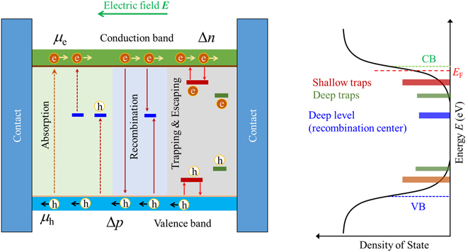
There are several time constants involved in the photodetection process. The response time is the measure of time raising and falling edges of a pulsed light in time. It is generally considered that a direct semiconductor responds faster than an indirect one, since the later involves the interaction of photon with phonon. The decay time is determined by the longer time scale among the carrier lifetime and the time τr for the carrier to transit across the channel area τr(= L 2/μV ds). In the presence of traps, a carrier can be captured at a rate ∝1/τt and released by the thermal excitation to the nearest energy band at a rate ∝1/τg. Consequently, the decay process corresponding to the emptying of the trapped carrier from shallow-level traps, has a much shorter escaping time than that of deep-level traps. Hence it is important to reduce the depth of the trap to achieve a fast decay speed. The bandwidth B is another important parameter for a photodetector that is defined as the cutoff modulated frequency of the incident light at which the photocurrent or responsivity is lowered by 3 dB under illumination. The bandwidth is usually inversely proportional to the response time and can be conveniently estimated via B ≈ 1/2πτ.
The specific detectivity D* is defined as
 ${D^*} = \sqrt {\left( {A\Delta f} \right)} {\rm{/NEP}}$
, where A is the area of the detector, Δf is the bandwidth used for the measurement of noise, and NEP = I
ph/P
eff
I
noise represents the incident power needed to produce a photocurrent equal to the noise current I
noise. In the case that short noise contributes predominantly to the noise-equivalent current,
 ${I_{{\rm{noise}}}} \approx \sqrt {2q{I_{\rm{d}}}\Delta f}$
, thus the specific detectivity
 ${D^ * } = R{\rm{/}}\sqrt {2q{I_{\rm{d}}}{\rm{/}}A}$
, where I
d is the dark current.
Reference Choi, Cho, Konar, Lee, Cha, Hong, Kim, Kim, Jena, Joo and Kim104
Thus it is desirable to have a semiconductor with relatively large band gap to obtain a detector with small dark current and high specific detectivity.
The spectral selectivity represents the cutoff wavelengths beyond which the response signal is comparable or smaller than the noise level. This is usually determined/limited by the band gap of a single photoactive material. Hence it is important to choose a proper photoactive material with different band gaps as the sensitizer to achieve an extended spectral selectivity.
IV. HYBRID PHOTODETECTOR WITH DIFFERENT SENSITIZERS
In contrast to bilayer or multilayer, photodetectors based on monolayer TMDCs can photoexcite electron–hole pairs without involving the slowly moving phonons, which allows faster switching between the light on and off states. However, the absorption efficiency is greatly reduced due to the atomic thickness of TMDC-based photodetectors, resulting in responsivity at the order of 1–102 mA/W in monolayer TMDCs with reduced defects, much smaller than the conventional materials of Si. Reference Perea-López, Lin, Pradhan, Iñiguez-Rábago, Laura Elías, McCreary, Lou, Ajayan, Terrones, Balicas and Terrones105,Reference Chang, Zhang, Zhu, Han, Pu, Chang, Hsu, Huang, Hsu and Chiu106 Integration of highly photoactive materials is desirable to improve the light absorption properties, and thus enhances the responsivity of the photodetector. As far as the sensitizers are concerned, the band structure has to well match the TMDCs to facilitate an efficient injection of carrier photogenerated in the sensitizer into TMDCs.
Sensitizers play a key role and are used to convert photons into electrical signals in photodetectors. 2D TMDC materials have recently attracted great attention as sensitizers in photodetectors due to their band gap changing from infrared to ultraviolet (UV) and their strong photon absorption. Reference Xia, Wang, Xiao, Dubey and Ramasubramaniam107,Reference Wen, Yin, He, Wang, Zhang, Wang, Shifa, Xu, Wang, Zhan, Wang, Jiang and He108 MoS2, as representative of TMDCs, has been extensively investigated as a photodetector. The photodetector based on the first-reported monolayer MoS2 exhibited a low responsivity of 7.5 mA/W at a laser power of 80 µW and good chemical stability. Reference Yin, Li, Li, Jiang, Shi, Sun, Lu, Zhang, Chen and Zhang109 However, the response time of monolayer MoS2 obtained by mechanical exfoliation method was relatively high (about 50 ms) due to the trapping of photocarriers. Reference Yin, Li, Li, Jiang, Shi, Sun, Lu, Zhang, Chen and Zhang109 The responsivity and specific detectivity of multilayer MoS2 existed in the range of 50–120 mA/W and 1010–1011 Jones for visible light, respectively, which was higher than that reported for monolayer MoS2. Reference Choi, Cho, Konar, Lee, Cha, Hong, Kim, Kim, Jena, Joo and Kim104,Reference Yin, Li, Li, Jiang, Shi, Sun, Lu, Zhang, Chen and Zhang109 But the responsivity and specific detectivity of phototransistors based on multilayer MoS2 were reduced to 0.09 mA/W and 5 × 10⁷ Jones for infrared, respectively. Reference Choi, Cho, Konar, Lee, Cha, Hong, Kim, Kim, Jena, Joo and Kim104 The responsivity of phototransistors can be improved to 880 or 106 A/W through p-PbS QDs decorating the surfaces of the monolayer or fewer-layers MoS2, respectively. Reference Lopez-Sanchez, Lembke, Kayci, Radenovic and Kis18,Reference Kufer, Nikitskiy, Lasanta, Navickaite, Koppens and Konstantatos30 The enhanced sensitivity of phototransistors benefited from the synergism between PbS QDs and MoS2. Similar results have also been found in other 2D materials, such as graphene, WS2, and WSe2. Reference Koppens, Mueller, Avouris, Ferrari, Vitiello and Polini16,Reference Kagan, Lifshitz, Sargent and Talapin26,Reference Yu, Zhang, Song, Zhang, Cao, Che, Dai, Yang, Zhang and Yao29,Reference Hu, Dong, Yang, Qiao, Yang, Deng, Yuan, Khan, Lan, Song and Tang38,Reference Chen, Qiao, Lin, Man Luk, Liu, Xu, Song, Xue, Li, Yuan, Yu, Pan, Ping Lau and Bao110 WS2 as another typical representative of TMDCs has relatively high carrier mobility, good thermal stability, no dangling bonds, and electrostatic integrity. Reference Huo, Yang, Wei, Li, Xia and Li111,Reference Zhang, Wang, Yang, Liu, Xu, Ning, Zak, Zhang, Tenne and Chen112 Consequently, WS2 has attracted wide attention due to its application in phototransistors and photodetectors. Reference Xue, Zhang, Liu, Liu, Song, Sophia, Liu, Xu, Xu, Wang, Zheng, Liu, Li and Bao1,Reference Yao, Zheng, Shao and Yang113 The photodetector based on the 2D multilayer WS2 nanoflakes obtained by the exfoliated method has been systematically investigated, with a low responsivity of 5.7 A/W, response time of <20 ms, and external quantum efficiency (EQE) of 1118%. Reference Huo, Yang, Wei, Li, Xia and Li111 Many strategies, such as QDs, NSs, and heterostructures, were used to improve the performance of photodetectors based on monolayer WS2.
A. Hybrids with QDs
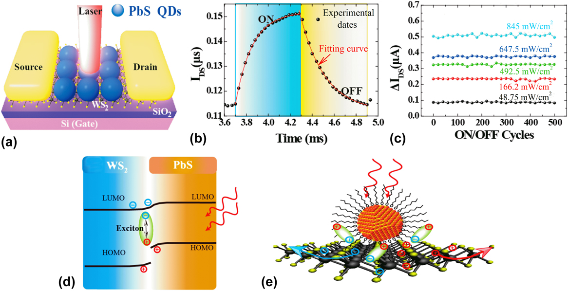
Semiconducting QDs such as CQDs are highly photosensitive with a size-tunable absorption and a selective range covering a broad spectrum from UV-visible up to mid-IR, which makes it an ideal sensitizer for hybrid photodetector with high responsivity and a wide spectral range. Indeed, great improvement of the light absorption and responsivity has been achieved by combining TMDCs with semiconductor QDs. Reference Kagan, Lifshitz, Sargent and Talapin26,Reference Konstantatos, Howard, Fischer, Hoogland, Clifford, Klem, Levina and Sargent114 By applying a layer of n-type PbS QDs atop the channel of n-type monolayer WS2 transistor, a responsivity of 14 A/W at 808 nm, specific detectivity of ∼4 × 10⁸ Jones, response time of 153 (rise) and 226 (decay) μs, response bandwidth of 400 Hz, and high stability are reported, as is shown in Fig. 4. Reference Yu, Zhang, Song, Zhang, Cao, Che, Dai, Yang, Zhang and Yao29 The increased light absorption due to the presence of PbS QDs layer and improved charge transfer process owing to the built-in electric field at the interface of QDs/WS2 heterojunction is considered to facilitate the enhancement of photodetection performance as illustrated in Fig. 4(d). When the n-type PbS QDs are applied atop the 10-μm length channel of p-type monolayer WSe2 transistors, the PbS/WSe2 shows great improvement in photodetection performance, with a responsivity up to 2 × 10⁵ A/W, specific detectivity up to 7 × 10¹³ Jones, and response time of 7 ms (rise) and 480 ms (decay) at V g = 0 under the illumination of 970 nm; particularly, the response spectral range is extended to 1400 nm. Reference Hu, Dong, Yang, Qiao, Yang, Deng, Yuan, Khan, Lan, Song and Tang38 In addition, owing to the well-matched band structure, CdS/ZnS core/shell-structured QDs-decorated monolayer WS2 demonstrates an extremely fast photogenerated carrier transfer process with a timescale of sub-45 fs from QDs to WS2. Reference Boulesbaa, Wang, Mahjouri-Samani, Tian, Puretzky, Ivanov, Rouleau, Xiao, Sumpter and Geohegan115
(a) Schematic diagram of WS2/PbS FETs. (b) Temporal photocurrent response of a WS2/PbS FET under red light irradiation of 845 mW/cm2. (c) Photocurrent of a photoswitch during 500 cycles with the relationship of irradiation. (d) Schematic of the band diagram of WS2/PbS heterostructure, and (e) schematic drawing shows change generation and transfer process under the illumination. Reference Yu, Zhang, Song, Zhang, Cao, Che, Dai, Yang, Zhang and Yao29 (Reprinted with permissions from Yu et al., Reference Yu, Zhang, Song, Zhang, Cao, Che, Dai, Yang, Zhang and Yao29 © 2017 American Chemical Society.)
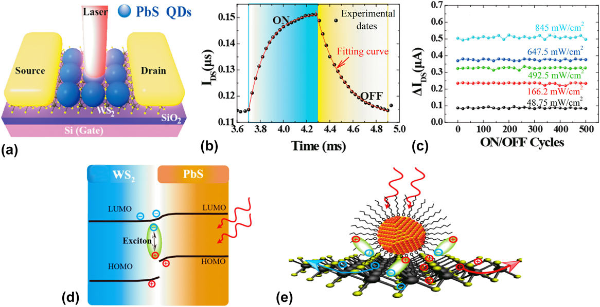
For the bilayer or multilayer, a sensitizer layer is also beneficial to the photodetection performance. Reference Kufer, Nikitskiy, Lasanta, Navickaite, Koppens and Konstantatos30,Reference Schornbaum, Winter, Schießl, Gannott, Katsukis, Guldi, Spiecker and Zaumseil116 It is reported that a layer of PbS QDs is atop the 3-μm length channel of bilayer MoS2 transistor with a responsivity as high as 2×10⁵ A/W, specific detectivity of 2–5×10¹¹ Jones at a back-gate biasing voltage of −60 V, and extension of the cutoff wavelength to NIR regime. Reference Kufer, Nikitskiy, Lasanta, Navickaite, Koppens and Konstantatos30 The working principle is shown in Figs. 4(d) and 4(e). The Fermi energy of PbS is higher than that of WS2, which results in some electrons rolling down from PbS to WS2. Hence an electric field forms in the interface between PbS and WS2, resulting in an efficient separation of electron–hole pairs excited by absorption photon in PbS. The electrons can be quickly collected in electrodes due to fast transfers in WS2. Therefore the photoresponse times are decreased.
B. Hybrids with NSs
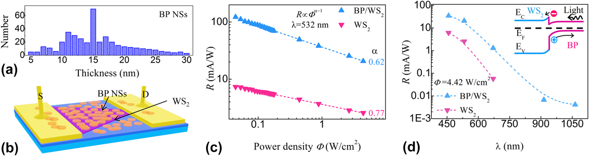
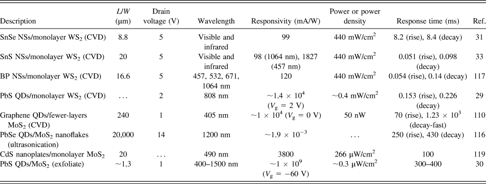
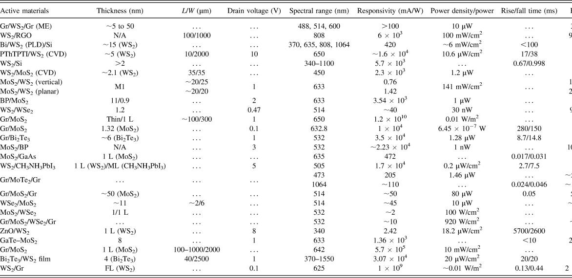
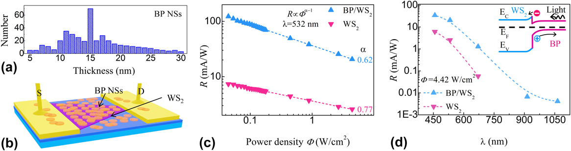
The layered NSs sensitizer shows advantages over the QDs in terms of contact area, surface flatness, and dangling bonds at the interface. Similar to QDs, a wide spectrum of layered materials, covering the UV to mid-IR, are available for effective candidate sensitizer. In addition, the layered NSs can be obtained by the green liquid-phase exfoliation in nontoxic solvents which is cost-effective and environmentally friendly. Layer structured NSs such as graphene, black phosphorus (BP), Bi2Te3, SnS, and SnSe have been successfully used as sensitizers for improving the performance of TMDC-based photodetectors. Reference Jia, Xiang, Wen, Yang, Hao and Liu31,Reference Jia, Li, Xiang, Wen, Bao, Feng, Yang and Liu33,Reference Chen, Qiao, Lin, Man Luk, Liu, Xu, Song, Xue, Li, Yuan, Yu, Pan, Ping Lau and Bao110,Reference Jia, Xiang, Mu, Wen, Yang, Hao and Liu117 In comparison with QDs, layer NSs with the atomic flat surface and free of dangling bonds have a larger contact area. Hence the responsivity and on/off switching speed can be improved owing to the larger hererojunction area and less-trapped states at the interface between layers NSs and TMDCs. By growing sheet-like CdS on monolayer MoS2 via chemical vapor deposition (CVD) technique, a responsivity of ∼3.9 A/W, response time of 100 ms, and extension of spectral selectivity to the NIR is achieved, which is attributed to the significant enhancement in absorption and efficient charge transfer between CdS and MoS2. Reference Zheng, Feng, Zhang, Chen, Liu, Qiu, Hasan, Tan and Hu118 In comparison with the pristine monolayer MoS2, the responsivity is being improved by a factor of 50 and is more than 100 times faster in response speed. Hybrid phototransistors based on monolayer WS2 exhibit considerable improvement in responsivity by a factor of 45 (99 mA/W @ 457 nm) for the sensitizer of liquid-phase exfoliated SnSe NSs, Reference Jia, Xiang, Wen, Yang, Hao and Liu31 by a factor of 20 (120 mA/W @ 532 nm) for the liquid-phase exfoliated BP NSs (Fig. 5). Reference Jia, Xiang, Mu, Wen, Yang, Hao and Liu117 Besides that, the extension of the response spectral range is observed in hybrid photodetectors of SnSe/WS2 and BP/WS2. Reference Jia, Xiang, Wen, Yang, Hao and Liu31,Reference Jia, Xiang, Mu, Wen, Yang, Hao and Liu117 Table I summarizes the photodetection performance of phototransistors based on 2D materials decorated with varied materials (QDs or NSs).
(a) Statistical distribution of thickness for BP NSs. (b) Schematic illustration of a BP/WS2 hybrid phototransistor. (c) Responsivity as a function of power density under illumination of 532 nm. (d) Variations of responsivity with the wavelength of the incident light. Inset is the schematic energy band diagram of BP/WS2. Reference Jia, Xiang, Mu, Wen, Yang, Hao and Liu117 (Reprinted with permissions from: Jia et al., Reference Jia, Xiang, Mu, Wen, Yang, Hao and Liu117 © 2017 Springer.)
Performance parameters of phototransistors based on 2D materials decorated with varied materials.

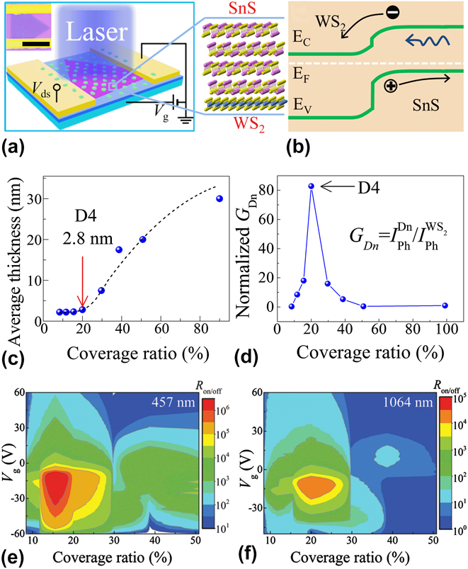
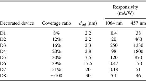
The light absorbance depends strongly on the thickness through which the incident light passes. On one hand, the sensitizer with a thickness approaching to the penetration depth would be desirable since it can maximally catch the input light. On the other hand, the increase in thickness of the sensitizer could prolong the diffusion time within the sensitizer; consequently decreasing the carrier concentration due to the increased recombination of photogenerated carriers, resulting eventually in a decrease in responsivity. Reference Jia, Li, Xiang, Wen, Bao, Feng, Yang and Liu33 The layered NSs should be as thin as possible as far as the charge screening effect, flexibility, and transparency of the devices are concerned. Reference Nasilowski, Mahler, Lhuillier, Ithurria and Dubertret120 The absorbance can be improved via increasing the area of sensitizers on TMDCs if the whole channel is under illumination. Jia et al. demonstrated that the responsivity of n-type monolayer WS2 can be greatly enhanced to ∼1.8 A/W (by four orders of magnitude) by applying a thin layer of p-type fewer-layer SnS NSs atop the channel of the transistor of monolayer WS2 (Fig. 6). Reference Jia, Li, Xiang, Wen, Bao, Feng, Yang and Liu33 They found that the incremental responsivity is also significantly raised upon increasing the coverage ratio of SnS NSs on WS2. However, this increment is maximized at a coverage ratio of ∼20% and suppressed at a higher coverage ratio. This is attributed to the takeover of vertical stacking instead of lateral spreading of SnS NSs by drop-casting at the cover ratio higher than 20%. The photoresponsivity is summarized in Table II under various coverage ratios and thicknesses of SnS. The SnS/WS2 hybrid photodetector also shows a very short response time of less than 100 μs due to the lack of trap state, high light on/off ratio up to 3 × 10⁵ owing to the built-in potential in the WS2/SnS p–n heterojunction, and a decent detectivity of 3.4 × 10¹⁰ Jones. In addition, the hybrid SnS/WS2 displays a decent detection performance in the NIR regime. It seems that the thinner the NS sensitizer is and higher the coverage ratio of the sensitizer on TMDCs, the higher the detection performance of the phototransistors based on TDMCs. By growing a full layer of fewer-layer SnSe2 sensitizer on monolayer MoS2 using CVD technique, Zhou et al. have managed to show a high responsivity of 9.1 × 10³ A/W and specific detectivity of 9.3 × 10¹⁰ Jones to the light of 500 nm, being nearly two orders of magnitude higher than that observed in monolayer MoS2 devices. Reference Xing, Nan, Chao, Hongyue, Qi, Xiaozong, Lin, Huiqiao, Jingtao, Jun, Jie and Tianyou121
(a) Schematic illustration of photodetector decorated by sensitizer, (b) energy level diagram for heterojunction between SnS and WS2, (c) average thickness of SnS NSs deposited on a WS2 monolayer, (d) normalized photocurrent augmentation of decorated devices, photoresponsivity as function of coverage ratio and gating voltage under (e) 457 nm and (f) 1064 nm. Reference Jia, Li, Xiang, Wen, Bao, Feng, Yang and Liu33 (Reprinted with permissions from Jia et al., Reference Jia, Li, Xiang, Wen, Bao, Feng, Yang and Liu33 © 2017 Royal Society of Chemistry.)

Photoresponsivity of WS2/SnS phototransistors with coverage ratio, average thickness of SnS NSs. Reference Jia, Li, Xiang, Wen, Bao, Feng, Yang and Liu33 (Reprinted with permissions from Jia et al., Reference Jia, Li, Xiang, Wen, Bao, Feng, Yang and Liu33 © 2017 Royal Society of Chemistry.)

C. Multilayers heterostructure
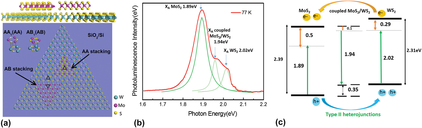
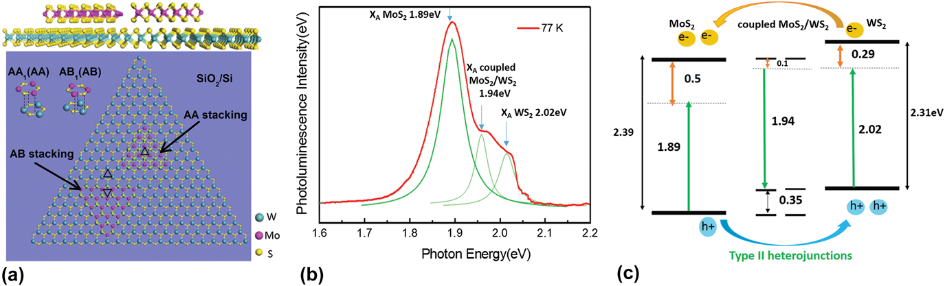
A full layer of sensitizer is preferable in terms of the coverage for the improvement of photodetection performance. Homostructure bilayer is the thinnest multilayer with higher absorption efficiency and reduced SBH compared with that of monolayer. However, the appearance of indirect electronic transition is adverse to the response speed. Hereostructures based on 2D layered materials can be readily achieved owing to weak van der Waals interlayer interaction and demonstrate novel properties and new phenomena, enabling the design of electronic and optoelectronic devices with novel and multifunction. Reference Deng, Luo, Conrad, Liu, Gong, Najmaei, Ajayan, Lou, Xu and Ye122,Reference Ai, Guan, Li, Yao, Chen, Zhang, Duan and Duan123 The van der Waals heterostructures exhibit many advantages such as: (i) ultrathin thickness which allowed for efficient electrostatic tuning of band structure, creating a new and relatively easy avenue for realization of electronic and optoelectronic devices with mechanical flexibility Reference Xue, Zhang, Liu, Liu, Song, Sophia, Liu, Xu, Xu, Wang, Zheng, Liu, Li and Bao1,Reference Deng, Luo, Conrad, Liu, Gong, Najmaei, Ajayan, Lou, Xu and Ye122 ; (ii) weak van der Waals interaction between two materials that are propitious to create high-quality heterojunctions without problems induced by lattice mismatch between two materials Reference Yang, Wang, Ataca, Li, Chen, Cai, Suslu, Grossman, Jiang, Liu and Tongay124,Reference Lee, Lee, van der Zande, Chen, Li, Han, Cui, Arefe, Nuckolls, Heinz, Guo, Hone and Kim125 ; (iii) the presence of carrier with prolonged lifetime at the interface of the van der Waals junction due to significant delocalization of photogenerated carrier facilitates an efficient separation of photoexcited electron–hole pairs, as well as a fast charge transfer across the interface in a timescale of subpicsecond, that can eventually enhance light emission and PV responses of heterostructured devices Reference Lee, Lee, van der Zande, Chen, Li, Han, Cui, Arefe, Nuckolls, Heinz, Guo, Hone and Kim125,Reference Zhang, Wang, Chen, Sun, Wu, Jia, Lu, Yu, Chen, Zhu, Xie, Yang, Shi, Xu, Xiang, Liu and Zhang126 ; (iv) strong light–matter interaction that can enhance the optical absorption properties and facilitate the creation of electron–hole pairs. Reference Hong, Kim, Shi, Zhang, Jin, Sun, Tongay, Wu, Zhang and Wang127,Reference Komsa and Krasheninnikov128 In the MoS2/WS2 heterostructure grown by CVD, a strong interlayers coupling is demonstrated, resulting in an efficient interlayer charge transfer and recombination of spatially separated excitons (Fig. 7). Reference Zhang, Wang, Chen, Sun, Wu, Jia, Lu, Yu, Chen, Zhu, Xie, Yang, Shi, Xu, Xiang, Liu and Zhang126 Because the minimum conduction and maximum valence band of WS2 is higher than that of MoS2 [Fig. 7(c)], electrons and holes excited by light trend to individually accumulate in the conduction band of MoS2 and the valence band of WS2, resulting in a built-in electric field positioned to MoS2. The interlayer radiative recombination of these separated carrier lead to the occurrence of an extra PL emission at 1.94 eV [Fig. 7(b)]. Photodetectors based on the heterostructure built with mechanically exfoliated 5-layer WS2 and 3-layer MoS2 displays a high electron mobility of 14 cm2/V s and high responsivity of 1.42 A/W. Moreover, the FET based on MoS2/WS2 heterostructure exhibits a self-driven photoresponsivity of 0.76 A/W and EQE of 149%, excellent rectifying effect, a bipolar behavior with an n-type behavior (on–off ratio of 104) under positive V sd, and a p-type behavior (on–off ratio of 10) under negative V sd = −10 V.
(a) Top and side views for atomistic illustration of vertical MoS2/WS2 bilayers; (b) PL spectra of heterostructure and Lorentzian fitting at 77 K; (c) band-gap alignment of MoS2/WS2 heterostructure Reference Zhang, Wang, Chen, Sun, Wu, Jia, Lu, Yu, Chen, Zhu, Xie, Yang, Shi, Xu, Xiang, Liu and Zhang126 (Reprinted with permissions from Zhang et al., Reference Ai, Guan, Li, Yao, Chen, Zhang, Duan and Duan123 © 2015 WILEY-VCH Verlag GmbH & Co. KGaA, Weinheim.)
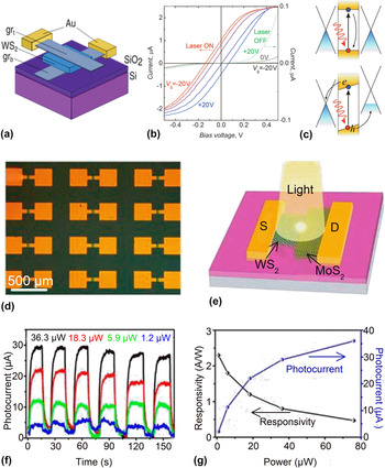
Cheng et al. have shown a responsivity of ∼0.6 A/W and a response time of less than 100 μs to green light for photodetector based on p–n vertical van der Waals heterojunction of monolayer PVD-WSe2 and exfoliated fewer-layer MoS2. Reference Cheng, Li, Zhou, Wang, Yin, Jiang, Liu, Chen, Huang and Duan129 A responsivity of 0.4 A/W to yellow light has been reported in p–n heterostructure of exfoliated fewer-layer BP and monolayer CVD-MoS2. Xue et al. have successfully synthesized the vertical multilayer MoS2/WS2 heterostructure by two-step CVD. Reference Xue, Zhang, Liu, Liu, Song, Sophia, Liu, Xu, Xu, Wang, Zheng, Liu, Li and Bao1 Flexible photodetector arrays based on vertical multilayer MoS2/WS2 heterostructure display a high photoresponsivity which can reach to 2.3 A/W under blue light (450 nm) and a good signal/noise ratio [shown in Fig. 8(f)]. Decent responsivities have also been achieved in the TDMCs heterostructure, such as MoS2/GaTe (responsivity of 1.365 A/W and EQE of 266%). Reference Yang, Wang, Ataca, Li, Chen, Cai, Suslu, Grossman, Jiang, Liu and Tongay124 For 2D heterostructure as sensitizer, a formation of the Schottky barriers at the interface of the heterostructure can result in a built-in electronic field improving the charge transfers at interface. Hence the performance of photodetection can be improved which is attributed to the efficient charge transfer at the interface of the heterostructure. The photodetection performance of photodetectors based on typical 2D heterostructures is summarized in Table III.
(a) Schematic of the Gr/WS2/Gr heterostructure, (b) (left axis) I–V curves taken under illumination at gate voltages from −20 (red) to +20 V (blue) after doping, (c) schematic band diagram for Gr/WS2/Gr heterostructure with and without a built-in electric field to separate photogenerated electron–hole pairs, Reference Britnell, Ribeiro, Eckmann, Jalil, Belle, Mishchenko, Kim, Gorbachev, Georgiou and Morozov130 (d) MoS2/WS2 heterojunction arrays, (e) schematic of MoS2/WS2 heterojunction phototransistor, (f) time-dependent photocurrent of MoS2/WS2 vertical heterostructure, (g) dependence of photocurrent and photoresponsivity on incident light power. Reference Xue, Zhang, Liu, Liu, Song, Sophia, Liu, Xu, Xu, Wang, Zheng, Liu, Li and Bao1 (Reprinted with permissions from (a–c) Britnell et al., Reference Britnell, Ribeiro, Eckmann, Jalil, Belle, Mishchenko, Kim, Gorbachev, Georgiou and Morozov130 © 2013 American Association for the Advancement of Science and (d–g) Xue et al., Reference Britnell, Ribeiro, Eckmann, Jalil, Belle, Mishchenko, Kim, Gorbachev, Georgiou and Morozov130 © 2016 American Chemical Society, respectively.)

Photoelectric performance of photodetector based on 2D heterostructures.

D. Other methods
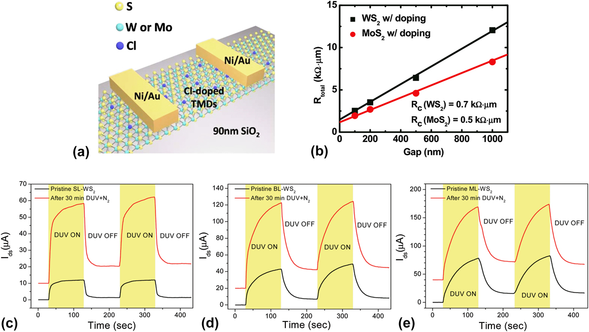
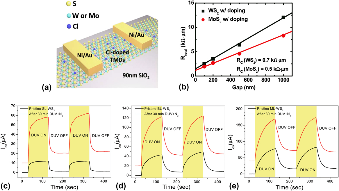
Besides the tailoring in photodetection performance by sensitizer, the contact between electrode and TMDCs is becoming a critical factor in restricting the development of high-performance optoelectronics. It is difficult to replenish all the photogenerated carriers reaching the contact interface due to the Schottky barrier caused by damage or the introduction of Fermi-level pinning. Previous substantial investigations have shown that only finite decrease of SBH occurs when using metals with different work function due to the Fermi-level pinning effect. Reference Tan, Fan, Zhou, Chen, Xu and Warner145,Reference Kyung-Ah, Janghwan, Kyeongjae and Suklyun146 The chemical doping of TMDCs is displayed to be an efficient method in reducing the SBH, such as lithium fluoride doping of WS2, Reference Khalil, Khan, Eom and Noh147 potassium iodide doping of WS2, Reference Iqbal, Iqbal, Khan, Kamran, Majid, Alharbi and Eom148 potassium doping of WSe2 and MoS2, Reference Fang, Tosun, Seol, Chang, Takei, Guo and Javey149 TiO2 doping of MoS2, Reference Kaushik, Karmakar, Nipane, Karande and Lodha150 and chloride molecular doping. Reference Yang, Majumdar, Liu, Du, Wu, Hatzistergos, Hung, Tieckelmann, Tsai, Hobbs and Ye151 Eom et al. developed a facile technique of illumination with deep UV light in a nitrogen environment for doping WS2. Reference Iqbal, Iqbal, Khan, Shehzad, Seo and Eom152 As shown in Fig. 9, the photocurrent can be drastically improved in monolayer, bilayer, and multilayer WS2 FETs. Another strategy was to achieve low contact resistance in TMDCs by using metallic 2D materials, such as graphene and NbSe2. Reference Britnell, Ribeiro, Eckmann, Jalil, Belle, Mishchenko, Kim, Gorbachev, Georgiou and Morozov130,Reference Tan, Fan, Zhou, Chen, Xu and Warner145 Graphene can be tuned to lower the contact resistance with TMDCs owing to the finite density of states in Dirac cones. Reference Shih, Wang, Son, Jin, Blankschtein and Strano153 Tan et al. utilized graphene as electrodes for WS2 and achieved a responsivity of 3.5 A/W in bilayer WS2 and 2.5 A/W in monolayer WS2 photodetectors under light (532 nm) with a power density of 3.8 × 10³ W/cm2. Reference Tan, Fan, Zhou, Chen, Xu and Warner145 The contact resistance at the electrode–semiconductor interface plays a key role in TMDC-based electronic devices. The low contact resistance can be obtained by tuning the Fermi level of graphene. Graphene is a finite density of state and highly stable and thus can be used as an ideal electrode material in TMDC-based devices.
(a) Schematic of Cl-doped fewer-layers WS2 back-gate FET, (b) transfer length method resistances of Cl-doped WS2 and MoS2, Reference Yang, Majumdar, Liu, Du, Wu, Hatzistergos, Hung, Tieckelmann, Tsai, Hobbs and Ye151 photocurrent response of (c) the SL WS2, (d) the BL WS2, and (e) the ML WS2 FET by 220-nm-dominant deep ultraviolet (DUV) illumination before and after the 30-min DUV + N2 treatment. Reference Iqbal, Iqbal, Khan, Shehzad, Seo and Eom152 (Reprinted with permissions from (a and b) Yang et al., Reference Yang, Majumdar, Liu, Du, Wu, Hatzistergos, Hung, Tieckelmann, Tsai, Hobbs and Ye151 © 2014 American Chemical Society and (c–e) Iqbal et al., Reference Iqbal, Iqbal, Khan, Shehzad, Seo and Eom152 © 2014 Royal Society of Chemistry, respectively.)
V. SUMMARY AND OUTLOOK
In summary, TMDCs have demonstrated great potential for high performance photodetectors due to their large absorption coefficient and high carrier mobility. To build photodetectors with high performance, TMDCs suffer from limited optical absorption due to the atomically thin nature and spectral selectivity in the visible regime due to the rather large band gap. Hybrid photodetectors based on TMDCs with various sensitizers could offer an effective and low-cost route toward not only the increase of absorption efficiency but also extension of the response range to the infrared regime. Although the hybrid photodetectors based on TMDCs have been investigated for many years, it is a long way before heterojunctions based on TMDCs can be largely applied. Fabricating and understanding physical mechanisms of large-scale flexible heterojunctions photodetection based on TMDCs are urgently needed. Moreover, the performance of photodetectors based on TMDCs can be enhanced by other strategies, such as strain engineering and tuning of the SBH. The contact between the electrode and TMDCs is one of the critical factors affecting the detection performance of the photodetector. It is a great challenge to efficiently integrate TMDCs and electrode materials due to the lack of dangling bonds. The Schottky barrier forms in the interface of metal/2D materials, resulting in transport issues and limit the performance and circuit design. Therefore an understanding of the physical picture is urgent for charge transport in Schottky carrier and improvement of performance of devices based on TMDCs.
Defects in 2D materials are hard to avoid and impact greatly on the photodetection performance. The existence of a considerable amount of deep-level trap state is detrimental to the response speed, particularly in prolonging the decay time. Hence it is desirable to develop feasible routes to move the deep-level to shallow-level trap state. Doping or alloying with different metals can tune the band gap thus altering the energy level of the defect state. Of late, monolayer TMDC materials have exhibited the property of ultrastrength, and the strain can reach to be as high as 25%. Thus it is possible to tune the defect level since the band gap can be continuously modulated by strain.
ACKNOWLEDGMENTS
The authors gratefully acknowledge the support from the National Natural Science Foundation of China (51571172, 11404280, 51672240, and 51571171), Natural Science Foundation for Distinguished Young Scholars of Hebei Province (E2017203095), Natural Science Foundation of Hebei Province (E2016203484 and A2015203337), and Research Program of the College Science & Technology of Hebei Province (ZD2017083 and QN2014047).