I. INTRODUCTION
Multilayered nanoscale materials have been shown to exhibit unique electrical,Reference Lu, Alexe, Scholz, Talelaev and Zacharias1–Reference Promnimit, Jafri, Sweatman and Dutta3 magnetic,Reference Albrecht, Hu, Guhr, Ulbrich, Boneberg, Leiderer and Schatz4 optical,Reference Wang, Masumoto, Someno and Hirai5, Reference Hiltunen, Seneviratne, Sun, Stolfi, Tuller, Lappalainen and Lantto6 and mechanical properties.Reference PalDey and Deevi7–Reference Wang, Misra and Hoagland9 In many of these applications, these materials are subjected to a variety of dynamic loading situationsReference Xie, Hoffman, Munroe, Singh, Bendavid and Martin10 such as wear and abrasion that lead to degradation and failure.Reference Graça, Colaço and Vilar11 Metal–ceramic nanolaminates have emerged as promising candidates as hard and tough coatings.Reference Martínez, Romero, Lousa and Esteve12–Reference Vyas, Li and Shen17 These materials exhibit a good combination of strength, hardness, and toughness.Reference Misra, Hirth and Hoagland8, Reference Wang, Misra and Hoagland9, Reference Chawla and Singh18–Reference Singh, Chawla, Tang and Shen22 To date, an understanding of deformation in these materials has been limited to static loading such as nanoindentationReference Oliver and Pharr23, Reference Bhattacharyya, Mara, Dickerson, Hoagland and Misra24 and micropillar compression.Reference Uchic, Shade and Dimiduk25, Reference Han, Phillips and Nix26 Although such methods provide a good fundamental understanding of the mechanical response and deformation mechanisms in these materials, a direct understanding of their deformation under wear and sliding conditions has not really been examined.
Scratch testing has been used recently to probe the tribological properties of multilayered materials.Reference Lu, Shi, Li, Luo and Mou14–Reference Vyas, Li and Shen17 Tribological behavior on the small scale has become increasingly important with the advent of micro- and nanomechanical devices. During scratch testing, both normal and tangential forces are applied during dynamic loading. Usually, an indenter tip is moved across the sample surface with increasing normal load. As the load increases, various fracture processes can occur such as cracking, delamination, coating spalling, and buckling.Reference Bull and Berasetegui27, Reference Larsson, Olsson, Hedenqvist and Hogmark28 The load at the onset of the fracture process is defined as the critical load.Reference Bull and Berasetegui27, Reference McAdams, Tsui, Pharr, Oliver, Baker, Ross, Townsend, Volkert and Børgesen29 Although the critical load is dependent on test conditions such as indenter geometry and loading rate,Reference Bull and Berasetegui27 it can be used as a good comparative tool for the evaluation of different materials tested under similar conditions.Reference Bertrand-Lambotte, Loubet, Verpy and Pavan30 In addition, scratch deformation can be quantified by of postscratch microstructural characterization.Reference Xie, Hoffman, Munroe, Singh, Bendavid and Martin10, Reference Lu, Shi, Li, Luo and Mou14, Reference Bertrand-Lambotte, Loubet, Verpy and Pavan30–Reference Briscoe, Pelillo and Sinha32
In this study, we have studied the scratch resistance of Al/SiC metal–ceramic nanolaminates and compared their behavior to that of monolithic Al and SiC films. The critical load and work of deformation were quantified. Postscratch fracture analysis was carried out using sections by focused ion beam (FIB) microscopy, as well as surface topography measurements from the diamond indenter itself.
II. MATERIALS AND EXPERIMENTAL PROCEDURE
The following three materials were compared in this study: Al/SiC multilayer (ML), Al thin film, and SiC thin film. Each of the samples was about 1-μm thick and grown on a Si (111) substrate using magnetron sputtering, as described elsewhere.Reference Chawla, Singh, Shen, Tang and Chawla19 The Al and SiC layers were each about 50- to 60-nm thick, with a total of 21 layers. Scratch testing was performed using a commercially available nanoindenter (XP; Agilent, Chandler, AZ). Multiple scratches were performed in each of the samples under load control. A constant loading rate of 2.5 mN/s and a sliding velocity of 10 μm/s were used for all samples. Scratch analysis was carried out with the Berkovitch indenter face moving through the surface, i.e., the face of the indenter was perpendicular to the scratch direction. After scratch testing, the scratches were analyzed using scanning electron microscopy (SEM) to analyze the scratch profile and to identify the point where film failure took place. The deformation under the scratch surface was analyzed by cross-sectional analysis using a dual beam FIB.
III. RESULTS AND DISCUSSION
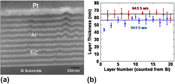
The microstructure of the Al/SiC nanolaminate is shown in Fig. 1. A total of 21 alternating layers of Al and SiC were grown on a Si (111) substrate. The Al thickness was 55 ± 4 nm, and SiC layers were 61 ± 2 nm thick. This corresponds to a volume fraction of Al of about 48%. A small degree of roughness is associated with the individual layers and is attributed to the columnar grain structure of the Al layers.
(a) Microstructure of Al/SiC nanolaminate on a Si (111) substrate (b) layer thickness distribution for Al and SiC.

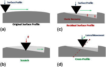
A schematic for typical scratch experiments is shown in Fig. 2. In the first segment, the reference surface of the sample is quantified by rastering the indenter over the surface at a very small load (100 μN). This is followed by a load-ramp scratch segment performed near the profiling trace. After the scratch segment, the indenter traces back the scratch length with a small load (100 μN) to estimate the residual deformation in the scratch. This measures the permanent deformation at any point in the scratch. Finally, in the fourth segment, a cross profile is carried out perpendicular to the scratch direction (100 μN) to obtain the width and profile of the scratch track. The cross profile was carried out on the scratch at a depth before the critical fracture event.
Schematic of scratch testing procedure used in this study.

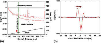
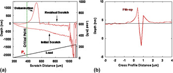
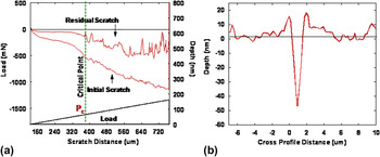
Figures 3–5 show representative scratch depth and applied load versus scratch distance for Al, SiC, and the nanolaminate. A cross profile for each of the representative scratches is also shown. Figure 3 shows the scratch and recovered profile for the Al film. Very little elastic recovery takes place and majority of the deformation is plastic. The critical load occurs at a load of about 125 mN. In the case of Al, this critical load represents the point at which the diamond indenter has penetrated through the film and makes contact with the Si substrate. Figure 4 shows a similar comparison for SiC. The film shows significant elastic recovery after scratch. Delamination is observed at relatively low critical loads, and the film debonds from the substrate easily. The scratch in the nanolaminate exhibits beneficial properties of the plastic and elastic layers, as shown in Fig. 5. A significant amount of elastic recovery takes place due to the SiC layers. The overall scratch depth is between that of pure SiC and Al.
(a) Scratch test on Al film showing the scratch penetration and residual morphology. The critical load corresponds to onset of film fracture. (b) Cross profile of scratch taken at a precritical scratch load of 10 mN. Significant pile-up is observed.

(a) Scratch test on SiC thin films showing the scratch penetration and residual morphology. (b) Cross profile of scratch taken at a precritical scratch load of 10 mN.

(a) Scratch test on Al/SiC nanolaminate showing the scratch penetration and residual morphology, with significant amount of elastic recovery. (b) Cross profile of scratch taken at a precritical scratch load of 10 mN.

A significant amount of quantitative information can be obtained from the scratch experiments. These include the critical load and displacement for failure (e.g., due to blistering or delamination), the work of elastic deformation, work of plastic deformation, width of scratch, and penetration depth of the scratch. It should be noted that careful postexperiment characterization of the scratch surface needs to be conducted to obtain a valid correlation to features on the depth/load versus scratch distance curves.
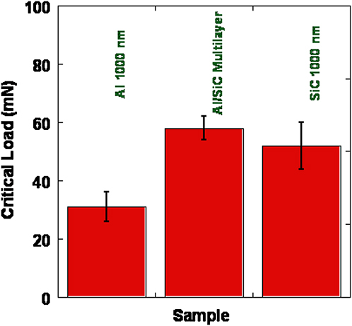
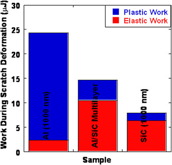
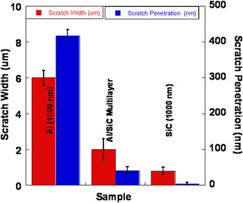
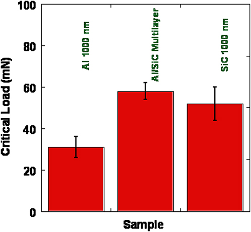
The critical loads were determined as the first discontinuity in the depth versus scratch distance curves. Average values of the critical load, for the three materials tested, are shown in Fig. 6. The nanolaminate materials exhibited higher critical loads than either Al or SiC. The nanolaminate benefits from strong and stiff SiC layers which are sandwiched between the highly plastic Al layers. This unique combination has also been shown to be quite flexible.Reference Chawla, Singh, Shen, Tang and Chawla19 The elastic and plastic work done on the samples during scratch, prior to film failure (critical load), was also quantified by measuring the area under the load versus displacement, as shown in Fig. 10. As can be seen from the graph, the work done for the ML is in between that of Al and SiC. Even with a high content of SiC, the nanolaminate can accommodate deformation by plastic deformation of the Al phase before delamination occurs. This gives the nanolaminate added scratch resistance over the monolithic SiC films. Also, unlike the Al film, the scratch does not penetrate through the entire film thickness, as shown in Fig. 7. All of these factors contribute to the improved scratch resistance of the ML. The scratch width and depth, Fig. 8, are also compared below critical load (10 mN) as indicators of scratch resistance. The composite response of the nanolaminate is observed here as well, as the scratch width and penetration are between that of Al and SiC.
Comparison of critical load for the various samples. The Al/SiC multilayer exhibits the highest critical load.
Comparison elastic work and plastic work of deformation for Al, SiC, and Al/SiC nanolaminate, obtained from the load–depth behavior during scratch testing. Note the high amount of recoverable work in the nanolaminate.

Comparison of scratch resistance of Al, SiC, and the nanolaminate in terms of scratch width and scratch penetration measured at a scratch load of 10 mN.

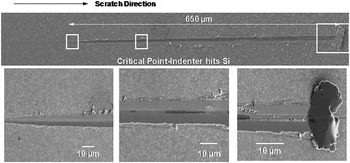
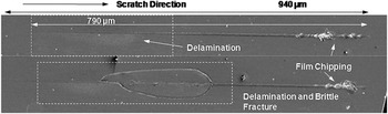
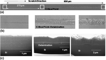
Postdeformation analysis was conducted by surface examination by SEM, as well as cross sections made by FIB. Representative surface images and cross sections for Al, SiC, and nanolaminate are shown in Figs. 9–11. In Al, Fig. 9, no obvious delamination of the film takes place although significant macroscopic plastic deformation takes place. Deformation proceeds by ploughing through and dragging of material.Reference Jardret, Oliver, Vinci, Kraft, Moody, Besser and Shaffer33 The critical load takes place a few hundred nanometers before hitting the Si substrate. The cross profile indicates that significant pile-up occurs on both sides of the scratch. No significant delamination was observed in Al films. In SiC, failure appears to be catastrophic as large chunks of the film fracture and are removed from the substrate, as shown in Fig. 10. As the loading further progresses, film chipping is also observed at higher loads. Higher elastic recovery and low pile-up was observed in the hard SiC films. The scratched surface and cross section in the nanolaminate is shown in Fig. 11. At and beyond the critical point, film blistering is observed which is related to the deformation of the delaminated film. At higher loads, the center of the scratch path remains bonded to the substrate implying a strong compressive stress, whereas the outer edges experience a combined local tensile/shear load that leads to film delamination. Besides film delamination, fracture of the individual layers and plastic deformation of Al were also observed.
Postscratch morphology of scratches in Al thin film imaged using scanning electron microscopy (SEM).

Postscratch morphology of scratches in SiC 1000-nm thin film with imaged using SEM. Clear delamination is visible in early stages of the scratch process.

Postscratch surface and FIB cross-sectional morphology of scratches in Al/SiC thin film imaged using SEM: (a) low magnification surface view, (b) higher magnification surface view, and (c) FIB cross-section. Clear delamination is visible at the critical load.

IV. SUMMARY
In this study, we have evaluated the mechanical response of metal–ceramic nanolaminates under scratch loading conditions. Al/SiC nanolaminate possesses better scratch resistance than its monolithic SiC and Al counterparts. Although Al thin films are too soft and the indenter penetrates through the film at small loads, SiC tends to delaminate from the Si substrate due to poor adhesion. The ML structure provides a compromise between the two materials by having a good interface and providing both strength and toughness against dynamic loading. Critical loads for fracture are highest for the multilayered structure. It can be concluded that metal–ceramic nanolaminates present significant potential to produce tough coatings for wear applications.
ACKNOWLEDGMENTS
The authors are grateful for financial support for this research from the National Science Foundation (DMR-0504781, Drs. A. Ardell, H.D. Chopra, and B.A. MacDonald, Program Managers). We also acknowledge the use of characterization facilities at the Center for Solid State Science at Arizona State University.