I. INTRODUCTION
Hydrogen has been considered as a future energy carrier. Reference Zuttel, Remhof, Borgschulte and Friedrichs1–Reference Kanan and Nocera3 Hydrogen production using solar-driven water splitting has a high potential to envision the approach of clean and sustainable energy supply system. This concept is satisfactory for on-site energy generation, storage, and utilization. An effective way of hydrogen production can be realized by photoelectrochemical (PEC) cell. The universal sunlight would benefit to generate electricity on-site of energy demand using semiconductor/electrolyte interfaced PEC cell. Therefore, high interests have been emerged to find an appropriate semiconductor material, which can effectively absorb the sunlight for long-term stability. Reference Lewerenz and Peter4–Reference Patel, Chavda, Mukhopadhyay, Kim and Ray6 If the transparent PEC system is performed, more possibility of on-site energy utilization can be realized.
The most conventional approach for solar fuel (H2) production using PEC water splitting applies a single semiconductor photoelectrode (photocathode) with a Pt counter electrode. The overall event of PEC is two hydrogen molecules production by the water reduction reaction upon the absorbed four photons; meanwhile, the water oxidation reaction induces one molecular O2 after taking four holes. Researchers have tried to alternate Pt metal electrode by the photoanode materials (e.g., n-Si, BiVO4, Fe2O3, MoS2, and SnS), which have a smaller band gap than that of the photocathode. In the aspect of photon utilization, transparent photocathode would allow to pass the photons reaching to photoanode. This transparent photocathode scheme would be considered for one promising approach to realize the theoretical solar to hydrogen efficiency limits of >25%. Reference Lewerenz and Peter4,Reference Patel, Chavda, Mukhopadhyay, Kim and Ray6–Reference Kim, Kaneko, Minegishi, Kubota, Domen and Lee13
Among metal oxides, Cu oxides such as CuO, Cu2O, and Cu4O3 are attractive because of their abundance, nontoxic and low cost features, affordable fabrication. Reference Zhang, Zhang, Xu, Yang and Huang14–Reference Samal and Koster23 Various Cu oxides have been reported by using TiO2 protected Cu2O film Reference Paracchino, Laporte, Sivula, Grätzel and Thimsen24 or CuO layer protected nanostructure of Cu2O. Reference Hu, Shaner, Beardslee, Lichterman, Brunschwig and Lewis2,Reference Luo, Steier, Son, Schreier, Mayer and Grätzel25 However, monoclinic CuO is known for the most stable among all phases of Cu oxides with a tunable band gap 1.1 eV–1.7 eV.
The performances of CuO photoelectrode involved PEC cell is chronologically summarized in Table SI, Supplementary Material (SM). In 1982, Koffyberg and Benko studied PEC cell with Li-doped CuO for photocurrent density (J PHOTO) of 0.44 mA/cm2 and notified a promise of CuO as photocathode. Reference Koffyberg and Benko26 Quite a long time later, CuO photocathode involved PEC cells were improved by nanostructure engineering to achieve J PHOTO values of 1.2–3.15 mA/cm2. Chinag et al. concluded that improved J PHOTO was because of an antireflective property of biological templated CuO nanowires. Reference Chiang, Epstein, Brown, Munday, Culver and Ehrman16,Reference Chiang, Chang, Liu, Tai and Ehrman27,Reference Chiang, Shin, Aroh and Ehrman28 Tenorite CuO nanorods grown by RF sputtering method was demonstrated to be the efficient photocatalyst for hydrogen production. Reference Artioli, Mancini, Barbieri, Quattrini, Quartarone, Mozzati, Drera, Sangaletti, Gombac, Fornasiero and Malavasi29 Following reports suggested that CuO photocathode would be stable for water splitting by applying various metal oxides, such as TiO2, Reference Jin, Zhang, Li, Li and Lu30 Al2O3, Reference Zhang, Liu, Zhou and Yan31 WO3, Reference Widiyandari, Purwanto, Balgis, Ogi and Okuyama32 SnO2, Reference Zheng, Wei, Wei, Xie and Wei33 ZnO, Reference Kargar, Jing, Kim, Riley, Pan and Wang34 and NiO Reference Kang, Chen, Li and Mu35 as protecting layer. However, the high potential of CuO photocathode has been still remained to find a route to produce high J PHOTO value by material-based architecture. Reference Patel, Chavda, Mukhopadhyay, Kim and Ray6,Reference Chiang, Shin and Ehrman36
Recently, Masudy-Panah et al. applied high purity CuO sputtering target for depositing the CuO films and applied for PEC cells to achieve J PHOTO of from 1.7 to 2.5 mA/cm2 by nanocrystal engineering. Reference Masudy-Panah, Siavash Moakhar, Chua, Tan, Wong, Chi and Dalapati37,Reference Masudy-Panah, Moakhar, Chua, Kushwaha, Wong and Dalapati38 Different from the conventional sputtering method, the reactive-sputtering would engineer the oxide stoichiometry. Moreover, reactive-sputtering approach is effective to form the compound oxide material with high yield and low energy use. By controlling of oxygen flow, various Cu oxide phases (CuO, Cu2O, and Cu4O3) can be actively controlled by using single Cu target. Reference Berg and Nyberg39–Reference Pierson, Thobor-keck and Billard41
From the fundamental point of view, CuO possesses extraordinary dielectric properties. Typical Mott insulator CuO can offer the tunable dielectric properties by engineering the crystalline properties. The relative dielectric constant value of CuO would be significantly modulated from 25 of polycrystalline to 3000 for a single crystalline. Moreover, Sarkar et al. demonstrated the extraordinarily high dielectric constant value of ∼104, which is almost independent from temperature (above 230 K) for kHz region. Reference Zheng, Sakurai, Okayama, Yang, Zhang, Yao, Nonaka and Xu42–Reference Sarkar, Jana, Chaudhuri and Sakata44 This substantial dielectric constant value enables the drift-assisted transport of photogenerated carriers through the wide space charge region. Reference Lewerenz and Peter4,Reference Ginley and Cahen5,Reference Van De Krol and Grätzel45
Here, we report the record-high J PHOTO value (6.4 mA/cm2) by using functionalized monoclinic CuO photoelectrode-embedded PEC system. A state-of-the-art reactive-sputtering method was applied to form various Cu oxides on to FTO-coated glass for large-scale affordable approach. Rapid thermal process (RTP) treatment effectively improved the transparency of Cu oxides and modulated the phase to be monoclinic CuO. Our finding is valuable to note (i) high J PHOTO value, (ii) control of Cu oxide phase formation, and (iii) high-reproducibility CuO photoelectrode for large-scale areas. Last but not the least, we demonstrated semitransparent PEC system.
II. EXPERIMENTAL DETAILS
A. Sample preparations
4 inch Cu target of purity 99.99% was reactively sputtered for forming the various phases of copper oxides at room temperature. Oxygen and argon were used as reactive and sputtering gases, respectively. Flow rate of Ar was 30 sccm fixed, while oxygen flow was varied from 1 sccm to 9 sccm. Three batches of samples were produced on the microscopic glass slides at various oxygen-flow-rate of conditions for Ar/O2 of 30/1 sccm (Batch-1), Ar/O2 of 30/5 sccm (Batch-3), and (c) Ar/O2 of 30/9 sccm (Batch-5). RTP-treatment is proven to be an effective method to tune metal oxide films. Reference Kim, Patel, Park, Ray, Jeong and Kim46–Reference Kim, Hong, Chang Park, Lee, Jeon and Kim48 To tune the Cu oxide film phase and crystallinity, RTP-treatment was performed. Twin samples were simultaneously prepared and treated by RTP at 550 °C for 10 min, under atmospheric condition. The ramping-up speed was applied by 200 °C/min. These samples were denoted as Batch-2 (RTP-treated Batch-1), Batch-4 (RTP-treated Batch-3), and Batch-6 (RTP-treated Batch-5), respectively.
For PEC cell fabrication, those batch samples were deposited on FTO-coated glass substrates. A commercial FTO-coated glass (735167, Sigma Aldrich) has a sheet resistance of 7 Ω/□. All substrates were chemically cleaned by a sequence of isopropyl alcohol, acetone, and distilled water using ultrasonication for 15 min. Sample surface was dried by blowing dry nitrogen after ultrasonication. Cleaned samples were inserted in a sputtering chamber using an inline loader. Krypton tape as shadow mask was applied to the FTO/glass substrates.
B. Sputtering
Base pressure of 5 × 10⁻⁵ Torr was obtained before flowing the reactive-sputtering gases. Working pressure of 5 mTorr was maintained by controlling the butterfly valve. 50 W of DC power was applied to Cu target. Deposition time of 20 min was fixed for fabricating all the samples. Substrate was rotated to ensure film uniformity of reactively formed Cu oxides.
C. Characterizations
Prepared samples were characterized by x-ray diffraction (XRD), field emission scanning electron microscopy (FESEM), surface profiler, UV–visible diffuse reflectance spectroscopy (DRS), Hall-measurements, PEC cell, and Mott–Schottky analysis. Structural properties of the prepared samples were characterized using XRD (SmartLab, Rigaku Corporation, Tokyo, Japan) with Cu Kα radiation (
 ${\lambda _{{{\rm K}_\alpha }}} = 1.540598\;{\AA}$
) in grazing mode with a glancing angle of 0.5° and step size of 0.05° at room temperature. The planar and cross-sectional morphologies were analyzed using a field emission scanning electron microscope (FESEM; JSM-7800F, JEOL Ltd., Tokyo, Japan) with 15 kV of field voltage, using an SE2 secondary detector. The thickness and average surface roughness of the deposited films were determined using a surface profiler (Dektak XT-E, Veeco, Plainview, New York). Optical properties were characterized using a diffused reflectance integrated sphere attached with UV–visible spectrophotometer (UV-2600, Shimadzu Corporation, Seoul, South Korea); characterization was performed by recording the transmission, absorbance and reflectance spectra of the thin films in the range 220–1400 nm.
D. PEC cell
The PEC measurements were carried out in a three electrodes cell attached to a potentiostat/galvanostat (PG-stat; ZIVE SP1, WonA Tech, Seoul, South Korea). Copper oxide-coated FTO, Ag/AgCl, and platinum gauze were connected to the working, reference, and counter electrodes of the PG-stat, respectively. Aqueous 0.1 M NaOH solution was used as electrolyte for all PEC measurements. High intensity white cooled light emitting diode (5800 K, ES Star Array, BXRA-56C0700-A, Bridgelux Inc., Livermore, California) was used as light source. Pulsed DC 18.1 V was applied to the LED unit. Light source was mounted on the quartz beaker facing CuO electrode. Light intensity (100 mW/cm2) was calibrated with a power meter (KM-SPM-11, KUSAM MECO, Mumbai, India). A scan rate of 20 mV/s with a sampling interval of 0.1 mV was set for recording the linear sweep voltammetry (LSV) (scan direction was positive to negative potential versus Ag/AgCl in all cases).
The measured potential V versus Ag/AgCl was converted to the reversible hydrogen electrode (RHE) scale according to the Nernst equation: E RHE = E Ag/AgCl + 0.059pH + E o Ag/AgCl where E RHE is the converted potential versus RHE, E o Ag/AgCl = 0.1976 at 25 °C, and E Ag/AgCl is the experimentally measured potential against Ag/AgCl reference.
The Mott–Schottky (1/C SC 2 versus V) analysis of photoelectrodes was carried out at an AC amplitude of 10 mV and a frequency range between 500 Hz – 5 kHz. DC potential was scanned from 0.4 V to −0.6 V versus Ag/AgCl with a sampling interval of 0.05 V.
III. RESULTS AND DISCUSSION
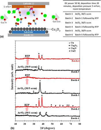
Cu oxide layers were deposited at room temperature by reactive-sputtering method with modulating the oxygen-flow-rate at 1 sccm (Batch-1), 5 sccm (Batch-3), and 9 sccm (Batch-5). The reactive-sputtering mechanism is presented in Fig. 1(a). Twin samples were simultaneously prepared and treated by RTP at 550 °C after sputtering. These RTP-treated samples are denoted as Batch-2 (RTP-treated Batch-1), Batch-4 (RTP-treated Batch-3), and Batch-6 (RTP-treated Batch-5). XRD analyses were performed on all samples, as shown in Fig. 1(b). Various Cu oxide phases were formed to demonstrate the potential of reactive-sputtering process for selective formation of Cu oxides. The crystallographic information file (CIF) 5000216, 9000603, 1000063, and 1526990 were referred to identify Cu, Cu4O3, Cu2O, and CuO phases, respectively.
(a) Schematic diagram of the reactive-sputtering method for Cu oxide film deposition. (b) XRD patterns of as-sputtered samples (Batch-1, Batch-3, and Batch-5) and RTP-treated samples (Batch-2, Batch-4, and Batch-6).

Changes of oxygen-flow-rate significantly affect the formation of Cu oxide phases. Batch-1 (oxygen-flow-rate at 1 sccm) showed the mixture amorphous phases of Cu4O3 and Cu2O. Batch-3 (oxygen-flow-rate at 5 sccm) showed the nanocrystalline Cu2O phase without any other phases. Batch-5 (oxygen-flow-rate at 9 sccm) has CuO phase only. Various phases of Cu oxides represent different crystalline properties such as Cu4O3, Cu2O, and CuO having a tetragonal, cubic, and monoclinic crystal systems, respectively. Reference Meyer, Polity, Reppin, Becker, Hering, Klar, Sander, Reindl, Benz, Eickhoff, Heiliger, Heinemann, Blasing, Krost, Shokovets, Muller and Ronning15 Therefore, it could be interesting to compare the morphology of CuO of the samples of Batch-2, Batch-4, and Batch-6 fabricated from different combinations of copper oxides. RTP-treatment substantially improved the crystalline properties and effective tune the phase formation. We found that Cu, Cu4O3, and Cu2O and their combinations can be converted to the nanocrystalline CuO phase by RTP-treatment (550 °C for 10 min, Fig. S1, SM). Among all samples, Batch-2 showed the most intensive XRD peaks, corresponding to the monoclinic unit crystal of CuO phase. Batch-6 also revealed a pure nanocrystalline CuO phase with relatively lowered intensity due to a thinner film formation (Fig. 2).
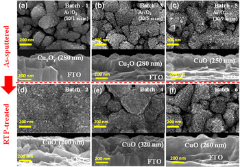
FESEM images of samples as-sputtered at room temperature for Ar/O2 flow rate (a) Ar/O2: 30/1 sccm (Batch-1), (b) Ar/O2 30/5 sccm (Batch-3), and (c) Ar/O2 30/9 sccm (Batch-5). After RTP-treated images of (d) Batch-2, (e) Batch-4, and (f) Batch-6. In each figure, the top image is a topography and the bottom image is a cross-section of the specimen on FTO/glass substrate.

This sequence of the reactive-sputtering and RTP-treatment strongly demonstrates the efficient scheme of monoclinic CuO formation from amorphous and mixture phases of Cu oxides (Cu4O3 and Cu2O). The conversion of CuO from various Cu oxides can be understood by the diffusion driven oxidation, which usually occurs at high temperature of 600–1000 °C. Reference Hapase, Gharpurey and Biswas49–Reference Poulston, Parlett, Stone and Bowker51 Meanwhile, we developed the efficient method of CuO formation with a low thermal-budget approach. This is an inherent advantage of reactive-sputtering and RTP, which may be applied for flexible CuO device applications.
Cu oxide films were observed by field emission scanning electron microscopy (FESEM). Top-view images were obtained at 100k× magnification and cross-sectional images were achieved at 50k× magnification, as shown in Fig. 2 (Fig. S2, SM). Significant surface morphological changes can be found by tuning the oxygen-flow-rate.
Interestingly, variation of nanoscale features can be attributed to distinct crystal structure as mentioned in the XRD description. Cross-sectional images revealed the consistent grown films of as-sputtered Cu oxide layers around 250–280 nm (Batch-1, Batch-3, and Batch-5). These observations point out little effect on Cu oxide film thickness with changes of oxygen-flow-rate. However, the oxygen-flow-rate significantly modulated the Cu oxide phases. According to the XRD analyses, Fig. 2(b) is cubic Cu2O structure and Fig. 2(c) is monoclinic CuO structure, respectively.
RTP-treatment is significantly effective to modulate the Cu oxide surface morphologies and convert their phases, as shown in Figs. 2(d)–2(f). Figure 2(d) (Batch-2, RTP-treated Batch-1) showed highly nanoscale crystalline CuO layer of 200 nm, which has been substantially reduced from as-sputtered 280 nm (Batch-1). This is attributed to the thermal oxidation-induced phase transformation of Cu oxide materials from Cu x O y [Batch-1, Fig. 2(a)] to highly crystalline and monoclinic CuO [Batch-2, Fig. 2(d)], as discussed in XRD analyses. Additionally, the RTP-treatment may cause amorphous CuO phase [Batch-4, Fig. 2(e)] from the nanocrystalline Cu2O [Batch-3, Fig. 2(b)]. It is worthy to note that the CuO formation is stable for Batch-5 and no noticeable surficial morphology changes occurred by RTP-treatment (Batch-6) but improved CuO crystallinity. The exact thickness of Cu oxide layers was obtained by surface depth profiler (Fig. S3, SM).
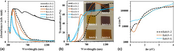
The optical properties of copper oxides films were investigated for absorbance (A) and transmittance (T), as shown in Figs. 3(a) and 3(b), respectively. Corresponding reflectance (R) tendencies are presented in Fig. S4, SM. RTP-treatment effectively varied A and T profiles by comparing as-sputtered samples (Batch-1, Batch-3, and Batch-5) and RTP-treated counterparts (Batch-2, Batch-4, and Batch-6). RTP-treatment is significantly effective to modulate the optical properties of Cu oxide films. Each sample has the inherent A and T profile, and is effectively controlled by RTP-treatment. A substantial optical change was observed from Batch-1, which has almost zero transmittance for all wavelengths (λ) and tuned to be semitransparent by RTP-treatment (Batch-2). Similarly, all RTP-treated samples showed the improved T values from as-sputtered samples. This clearly indicates the effect of oxygen concentration to control the proportional T value improvement by enhanced oxygen flows. By controlling the oxygen flows, various Cu oxide films can be formed, which induces inherent optical profiles according to the different stoichiometry. RTP-treatment is effective to allow the transparency to Cu oxide films. T profiles of Batch-2, Batch-4, and 6 gave average transparency of 16, 18.5 and 43% for visible photons (400–800 nm) to enable the semitransparent feature. It is mainly attributed to the changes in phases of Cu oxides as discussed with XRD and FESEM analyses.
Optical properties of the prepared samples of various copper oxides. (a) Absorption, (b) transmittance spectra, and (c) absorption co-efficient. Photograph of the prepared samples on glass substrate is shown in the inset of (b).

It is reasonable to investigate the effect of RTP-treatment by absorption profiles. Absorption coefficient (α) of the various featured Cu oxide films were estimated using the relation,
 $\alpha = {1 \mathord{\left/ {\vphantom {1 d}} \right. \kern-\nulldelimiterspace} d}\ln \left( {{{{{\left( {1 - R} \right)}^2}} \mathord/{\left {\vphantom {{{{\left( {1 - R} \right)}^2}} T}} \right. \kern-\nulldelimiterspace} T}} \right)$
, where d is the thickness of the film. Calculated α values as a function of photon energy (hν) are shown in Fig. 3(c). Here, h and ν are the Planck's constant and photon frequency, respectively. We can see all samples having, α values greater than 4 × 104 cm−1 for hν greater than 2 eV confirming that a very thin (250 nm) film is enough to absorb visible spectrum of the sunlight.
Further investigation was performed by Tauc plot analyses (Fig. S5, SM). It is worthy to note that E g value varies according to the various morphological and crystalline features of the CuO films. Batch-2 showed the higher E g value (1.7 eV) compared to other reports (Table SI, SM), to indicate the feature of our CuO film. Other Cu oxide films have even higher E g values of 1.8 and 1.85 eV for Batch-4 and Batch-6, respectively.
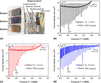
The various Cu oxide films were applied to FTO-coated glass as a working electrode of PEC cells. The developed samples are shown in Fig. 4(a), where 7 × 7 mm of active area can be seen. Cu oxide-coated electrode was immersed (up to marked line) into the aqueous 0.1 M NaOH electrolyte for recording PEC responses. The PEC cell (as shown in a photograph) contains a working electrode (CuO/FTO), a counter electrode (platinum gauze), and a reference electrode (Ag/AgCl).
(a) Photography of developed samples (marked region is the active area of CuO photocathode) and PEC cell system. Photoresponses of as-sputtered (Batch-1, Batch-3 and Batch-5) and RTP-treated (Batch-2, Batch-4, and Batch-6) samples prepared at various oxygen-flow-rates (b) 1 sccm, (c) 5 sccm, and (d) 9 sccm. J–V curves were obtained at room temperature by pulsed-illumination of 100 mW/cm2.

LSV photoresponses were measured from various Cu oxides of as-sputtered (Batch-1, Batch-3, and Batch-5) and RTP-treated samples (Batch-2, Batch-4, and Batch-6), as shown in Figs. 4(b)–4(d). Batch-1 and Batch-3 gave relatively low photoresponses (J PHOTO) because of its amorphous properties. Meanwhile, Batch-5 offered a meaningful J PHOTO value (1.75 mA/cm2) at 0.3 V versus RHE, which is attributed to the nanocrystalline CuO phase [Fig. 4(d)]. Substantially improved photoresponses were obtained by RTP-treatment, as shown in Figs. 4(b)–4(d).
Various semitransparent CuO-phase photocathodes (Batch-2, Batch-4, and Batch-6) provided generally improved PEC performances from as-sputtered samples (Batch-1, Batch-3, and Batch-5). The enhanced J PHOTO profiles for negative potential (cathodic) direction (from 0.7 V to 0.2 V versus RHE) indicate that these CuO samples are p-type for majority carrier transport. Batch-2 offered the highest J PHOTO value (6.4 mA/cm2) at an applied potential of 0.3 V versus RHE. This value is the record-high J PHOTO for the nanocrystalline monoclinic CuO photocathode, compared to other reported values (Table SI, SM). Similarly, Batch-4 and Batch-6 provided the improved J PHOTO values of 5.2 mA/cm2 and 5.6 mA/cm2, respectively. The obtained excellent photoresponses are attributed to the high α of CuO samples due to the RTP-treatment. In addition, RTP-treatment not only improved J PHOTO amplitude but also rendered the remarkably low dark current (J D). This confirms the quality interface formation between CuO film and FTO-coating layer. This is very promising feature of CuO photocathode for PEC cell applications to provide high J PHOTO value with a suppressed J D value, which is mainly attributed to the fair diode junction formation after RTP process (Fig. S6, SM).
Moreover, the development of transparent CuO photocathode would provide enhanced PEC performances and wide applications for life as transparent PEC system. The photocathode of Batch-2 was traced for the prolonged illumination condition, as shown in Fig. S7, SM. The J PHOTO value was decreased by 1.2 mA/cm2. A further improvement may be achieved by applying a functional protective metal oxide layer such as TiO2 or NiO onto CuO film to provide long-term stability and render a high potential value. Reference Hu, Shaner, Beardslee, Lichterman, Brunschwig and Lewis2,Reference Kang, Chen, Li and Mu35,Reference Patel, Kim and Kim52,Reference Kim, Patel and Kim53 In addition, atomically thin n-type MoS2 coating layer can be considered for long-term stability and the enhanced performance of CuO photocathode. Reference Morales-Guio, Tilley, Vrubel, Grätzel and Hu54–Reference Lukowski, Daniel, Meng, Forticaux, Li and Jin56
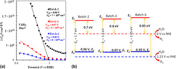
To investigate the band edges according to the RTP, Mott–Schottky analyses were performed for Batch-2, Batch-4, and Batch-6. As shown in Fig. 5(a), almost similar flat band potential (V FB versus RHE) values (0.95–0.97 V) were achieved by the linear fit of 1/C 2 versus V plots. Meanwhile, it is worthy to note that Batch-2 provided the relatively large change of capacitance, which is strongly attributed to the low-level acceptor carrier concentration (N A) of 7 × 1019 cm−3, compared to 3 × 1020 cm−3 (Batch-4) or 8 × 1020 cm−3 of (Batch-6). And thus, Batch-2 sample has low defect-related carrier loss, resulting in the highest current density value among the samples.
(a) Mott–Schottky characterization of CuO photocathode of Batch-2, Batch-4, and Batch-6. (b) Estimated energy band edges. The energy band edges were projected for reduction level (0 V versus RHE) and oxidation level (1.23 V versus RHE).

The conduction band edge (E C) is presented in Fig. 5(b), which shows that different E C positions. It is interesting to note that E C level of CuO photocathode can be modulated from 0.7 to 0.85 V versus RHE by changing the O2 flow rates to suggest the possibility of improved performances of CuO films.
IV. SUMMARY AND CONCLUSIONS
In summary, we developed semitransparent PEC cell system by using a functional CuO film as a working electrode. This monoclinic CuO film-embedding PEC cell provided the record-high photocurrent density (6.4 mA/cm2) at an applied potential of 0.3 V versus RHE. A state-of-the art sputtering method was applied to achieve functional CuO films and further RTP-treatment showed the promise of monoclinic CuO formation. High energy band gap values of Cu oxides can be actively achieved by modulating the sputtering and RTP, which is substantially useful to engineer band edges for PEC cells. This semitransparent CuO photocathode would be a pivotal entity for realizing transparent PEC system with enhanced PEC performances.
Supplementary Material
To view supplementary material for this article, please visit http://dx.doi.org/10.1557/jmr.2016.364.
Performance comparison of developed presented samples, Photographs of prepared samples, field emission scanning electron microscopy image taken at 20k× magnification, surface profiler measurements, reflectance and Tauc plots, Mott–Schottky analysis, and references.
ACKNOWLEDGMENTS
The authors acknowledge the financial support of the Korea Institute of Energy Technology Evaluation and Planning by the Ministry of Knowledge Economy (KETEP-20133030011000), Basic Science Research Program through the National Research Foundation (NRF) of Korea by the Ministry of Education (NRF-2015R1D1A1A01059165), and Korea Research Fellowship Program through the NRF by the Ministry of Science, ICT and Future Planning (NRF-2015H1D3A1066311). M. Patel and H. Kim have equally contributed to this work.