I. INTRODUCTION
Since O’Regan and GrätzelReference O’Regan and Grätzel1 first reported the dye-sensitized TiO2 solar cell with conversion efficiency of over 7% in 1991, the photoelectrochemical cells (PECs) based on metal oxide semiconductor [titanium dioxide (TiO2), zinc oxide (ZnO), tin dioxide (SnO2)] nanoelectrodes have attracted more and more attention. However, the band gaps of TiO2, ZnO and SnO2 are so large (usually greater than 3 eV) that they can only absorb a small part of visible light. To enhance the absorption in visible light, it is necessary to sensitize the metal oxide semiconductor nanoelectrodes. As a result, many sensitizers have been explored and dye sensitizers have been intensively studied. In addition to dye sensitizers, semiconductors with narrow band gaps have recently attracted much attention due to their excellent properties, such as higher absorption, greater stability and adjustable band gap.Reference Hossain, Koh and Wang2
Zinc oxide (ZnO) is regarded as an alternative candidate for photoanode material, because of its suitable conduction band (CB) locationReference Rawal, Sung, Moon, Shin and Lee3 and high electron mobility [205–300 cm2/(V s) for bulk ZnO and 1000 cm2/(V s) for single nanowire].Reference Tiwana, Docampo, Johnston, Snaith and Herz4 Moreover, ZnO can be tailored to various morphologies and nanostructures with high crystallinity under mild condition. It iseconomical, abundantly available in nature and easily prepared due to its ease of crystallization and anisotropic growth. It has hexagonal wurtzite and polarity in the c-axis direction. And as for the ZnO nanorod, it has an internal electrical field in the direction of the c-axis that facilitates charge transport and suppresses the recombination of injected electrons.Reference Law, Greene, Johnson, Saykally and Yang5 When it is used as photoanode in quantum dot (QD)-sensitized solar cells, it has higher electronic mobility that would be favorable for electron transport, with reduced recombination loss.Reference Chen, Li, Liu and Zhu6
ZnO has various morphologies, such as ZnO nanowire array, ZnO nanorod, ZnO nanoparticle, and ZnO double-layer structure.Reference Ouyang, Hu, Bai, Lv, Zhang, Ma and Chen7 When ZnO grows in a petri dish, because of the reason that during the growth process, solvent is affected to a certain extent by evaporation, leading to increase of concentration of the solution, it results in the appearance of ZnO double-layer structure. When ZnO grows in a sealed beaker, it mainly generates nanoflowers structures that consist of ZnO nanorods. The performance of the solar cells is associated with the morphology of ZnO.
Up to now, many methods have been explored for the preparation of ZnO nanostructure, such as precipitation method, sol-gel method, microemulsion method, hydrothermal method, electrochemical synthesis, physical vapor deposition, chemical vapor deposition, and so on. Among these methods, hydrothermal methodReference Chen and Chuang8 is a simple, low-cost, low-temperature, and manageable, method with high repeatability and it is suitable for production on a large scale. Patil et al.Reference Patil and Singh9 used electrodeposition technique to deposit vertically aligned ZnO nanorod thin films, and assembled cadmium sulfide (CdS) quantum dots-sensitized solar cells (QDSSCs). Guo et al.Reference Guo, Diao and Cai10 used hydrothermal method to obtain perpendicularly oriented ZnO nanorod array film, and assembled dye-sensitized solar cells (DSSCs); the overall solar energy conversion efficiency reaches 2.1%. Wonjoo Lee et al.Reference Lee, Min, Dhas, Ogale and Han11 used hydrothermal method for the preparation of ZnO nanorods, and formed CdS quantum dots (QDs) on the vertically aligned ZnO nanorods electrode by chemical bath deposition. In application of the QDSSCs, a power conversion efficiency of 0.54% under air mass 1.5 condition (80 mW/cm2) was achieved. Jing Chen et al.Reference Chen, Lei, Li, Zhang, Cui, Wang and Deng12 used hydrothermal method for the preparation of ZnO nanorod films, and deposited cadmium (II) selenide (CdSe) QDs on the ZnO nanorods by the electrophoreic deposition method. A maximum power conversion efficiency of ∼1% (0.98%) is achieved for the flexible QDSSC. Thambidurai et al.Reference Thambidurai, Muthukumarasamy, Sabari Arul, Agilan and Balasundaraprabhu13 used hydrothermal method for the preparation of ZnO nanorods, and deposited CdS quantum dots onto ZnO nanorods by dip coating method. The efficiency of the fabricated CdS quantum dot-sensitized ZnO nanorod-based solar cell is 0.69%.
In this work, we first used titanium tetrachloride (TiCl4) pretreatment to avoid the direct contact of electrolyte and fluorine-doped tin oxide conducting glass (FTO), and decrease the recombination probabilities. Then we fabricated a smaller-particle seed layer prior to growing ZnO nanostructure. Through this method, we obtain flower-like ZnO nanostructure that was composed of smaller diameter ZnO nanorods, so the surface area of ZnO is larger, and the amount of CdS QDs adsorbed on ZnO is larger too. We prepared ZnO nanorods using a low-cost, low-temperature hydrothermal method. Finally, we deposited CdS QDs on the ZnO nanorods by successive ionic layer adsorption and reaction (SILAR) method. Eventually, we achieved slightly higher efficiency than those from other works.
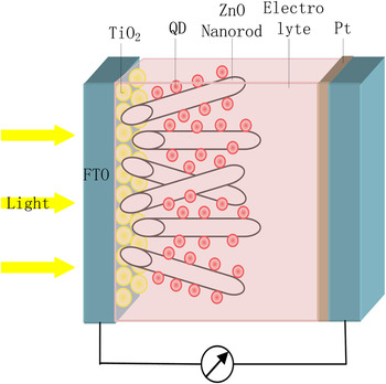
For enabling easy understanding of the cell structure, I provide a schematic diagram of the multilayer solar cell device in Fig. 1.
A schematic diagram of the multilayer solar cell device.

II. EXPERIMENTAL
A. Preparation of ZnO nanorods
In our experiment, we used the hydrothermal method for the preparation of ZnO nanostructure, FTO glass was used as the substrate. First, FTO glass substrates were ultrasonically soaked in deionized water, acetone, and absolute ethanol subsequently. Then the FTO glasses were soaked into the TiCl4 solution with the concentration of 0.04M for 30 min at 70 °C. After that the FTO glasses were sintered at 450 °C for 30 min. This process is called TiCl4 pretreatment.
When the FTO glasses cooled down to room temperature, 0.01 M zinc nitrate hexahydrate [Zn (NO3)2·6H2O] aqueous solution was added dropwise to them. When the FTO glasses became dry, we put them into muffle furnace, heating at 450 °C for 30 min. This process made a smaller-particle seed layer appear on FTO glasses.
After the FTO glasses cooled down to the room temperature, we attached nonstick tape on the surface of FTO glasses, leaving an area of 0.5 × 0.5 cm.
As in the case of synthesis process of ZnO nanorods, a mixture of Zn(NO3)2·6H2O (0.05 M) and C6H12N4 hexamethylenetetramine (HMTA) (0.05 M) solution (50 mL) was used as the precursor solution. This transparent solution was transferred to the laboratory beaker. Then the above FTO glasses were put horizontally into the solution, sealing the beaker mouth with saran wrap. The beaker was heated at a constant temperature of 95 °C for 20 h in a regular laboratory oven. Then the beaker was removed from the laboratory oven, after it cooled down to room temperature, the thin films on FTO glasses were thoroughly washed with deionized water and dried by nitrogen (N2).
B. Synthesis of CdS QDs
The SILAR method Reference Shi, Xue, Li, Zhao, Qu and Li14 was used to assemble CdS QDs onto the as-prepared photoanodes. The particle size of QDs was controlled by adjusting the deposition cycles. The as-prepared films were first immersed into the cadmium nitrate [Cd(NO3)2] aqueous solution (0.3 M) for 5 min, rinsed with absolute ethanol. Then they were dipped in the sodium sulfide (Na2S) aqueous solution (0.3 M) for another 5 min and rinsed again with methyl alcohol. The temperature of these processes was controlled at 30 °C, deposition cycles range was from 1 to 10.
C. Cell fabrication
The CdS quantum dots-sensitized ZnO nanorods electrode was incorporated into thin-layer sandwich-type cells with platinum (Pt)-coated FTO conducting glass as the counter electrode, a spacer film, and an electrolyte solution. Here, we used polysulfide electrolyte, which contains 0.5 M Na2S, 2 M S, and 0.2 M potassium chloride (KCl).Reference Lee and Chang15 The photoanode and Pt-coated FTO were separated by a 45-μm thick hot-melt spacer. The working area of the sample is 0.25 cm2.
D. Measurements and characterization
The morphologies of the ZnO nanostructure were examined by the scanning electron microscopy (SEM) system. The crystallinities of the ZnO nanostructure and CdS quantum dot-sensitized ZnO nanorods were investigated using x-ray diffraction (XRD). The photocurrent-voltage (I-V) curves were measured by the electrochemical workstation under an illumination of xenon lamp. The irradiance is 100 mW/cm2, which was measured by a radiometer (FZ-A, Photoelectric Instrument Factory of Beijing Normal University, Beijing, China).
III. RESULTS AND DISCUSSION
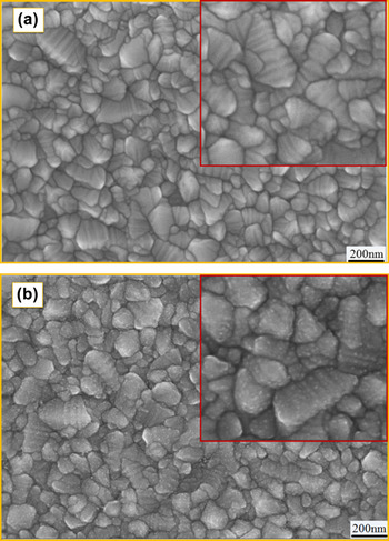
For avoiding the direct contact of electrolyte and FTO, and decreasing the recombination probabilities, we used TiCl4 pretreatment. As shown in Fig. 2, after the TiCl4 pretreatment, a layer of TiO2 nanoparticles grew on the FTO, they had diameter of several nanometers.
SEM patterns of (a) FTO electrode and (b) TiCl4-modified FTO electrode.

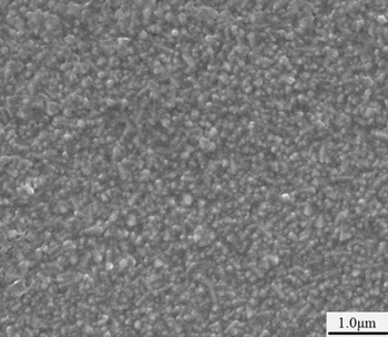
It has been hypothesized that by growing a layer of small particles of ZnO seeds prior to the growth of ZnO, we can get ZnO nanostructure that have good orientation, and small diameter size.Reference Song, Yu, Xie, Sun, Ling and Du16 So in our experiment, prior to the growth of ZnO, we first prepared ZnO seeds layer on the FTO conducting glass, as shown in Fig. 3. As we can see from Fig. 3, the particle size of ZnO seeds layer is about 100 nm. ZnO seeds layer is used as the nucleation site for the growth of well-oriented ZnO nanorods.
SEM image of ZnO seeds layer.

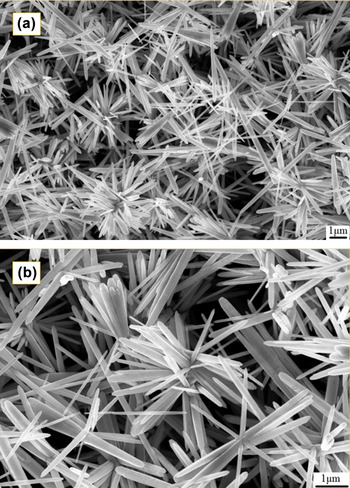
Thereafter, we grew ZnO nanostructure on the as-prepared ZnO seeds layer. Figure 4 shows the SEM images of ZnO. Figure 4(a) shows low-resolution SEM image and (b) high-resolution SEM image. We find that ZnO grown in this method has flower-like structure that is composed of ZnO nanorods, but the ZnO nanorods have diameter ranging from 100 to 200 nm; compared with those that have not been grown on the seeds layer, they have smaller diameter size.
SEM images of (a) low-resolution and (b) high-resolution ZnO nanostructure.

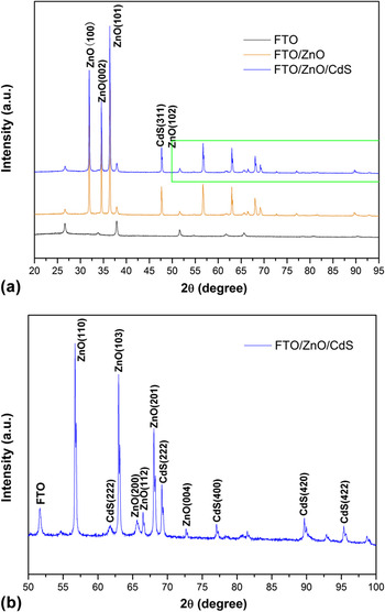
Figure 5 shows the XRD patterns of (a) FTO, FTO/ZnO and FTO/ZnO/CdS electrodes, and (b) the green box in (a) with 1000 times amplification. XRD results show that ZnO nanorods, and CdS quantum dot-sensitized ZnO nanorods exhibit hexagonal structure. The XRD spectra of FTO/ZnO revealed a (002) reflection, indicating that the grown ZnO nanorods had a high degree of c-axis orientation. In XRD spectra of FTO/ZnO/CdS, especially in (b), the green box in (a) with 1000 times amplification, we find some cubic CdS phases, suggesting CdS quantum dots have been successfully assembled onto the ZnO photoelectrode.
(a) XRD of FTO, FTO/ZnO and FTO/ZnO/CdS electrodes and (b) XRD of the green box in (a) with 1000 times amplification.

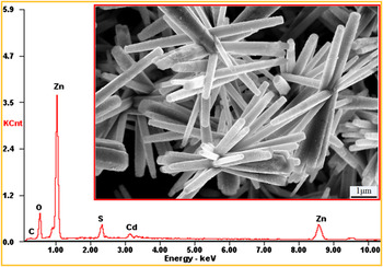
Figure 6 shows the energy-dispersive x-ray spectroscopic (EDX) pattern of CdS-sensitized ZnO nanorods with 6 SILAR cycles, the inset in the red box is the corresponding SEM image. From the SEM image, we find the surface of ZnO nanorods becoming rough. Comparing with the EDX pattern, we can prove the rough particles on the surface of ZnO to be CdS quantum dots, suggesting CdS quantum dots have been successfully assembled onto the ZnO photoelectrode.
SEM image and EDX pattern of CdS-sensitized ZnO nanorods with 6 SILAR cycles.

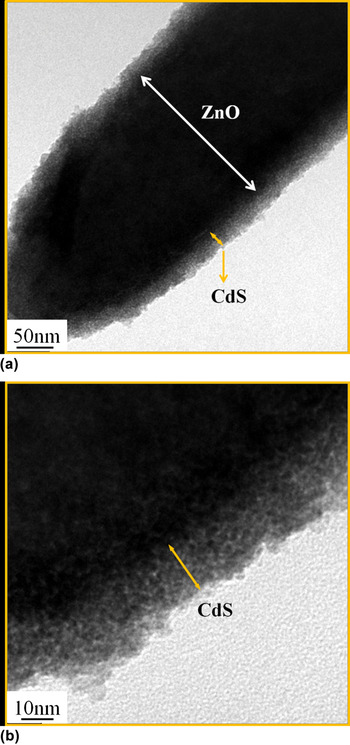
The TEM patterns of CdS-sensitized ZnO nanorods with 6 SILAR cycles are displayed in Fig. 7(a) low-resolution and (b) high-resolution. We can see clearly that CdS quantum dots adsorb uniformly onto the ZnO nanorod.
TEM patterns of CdS-sensitized ZnO nanorods with 6 SILAR cycles: (a) low-resolution and (b) high-resolution.

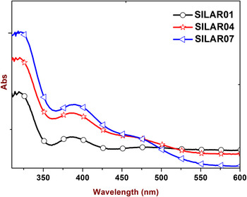
Figure 8 shows the UV-Vis absorption spectra of CdS-sensitized ZnO nanorods with 1 SILAR cycle, 4 SILAR cycles, and 7 SILAR cycles. From the UV-Vis absorption spectra, we discover the absorption edge shifts toward longer wavelength along with the increase in SILAR cycles.
UV-Vis absorption spectra of CdS-sensitized ZnO nanorods with 1 SILAR cycle, 4 SILAR cycles, and 7 SILAR cycles.

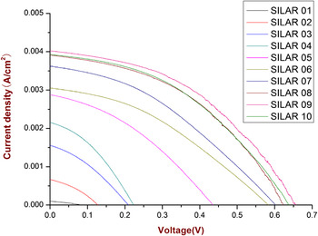
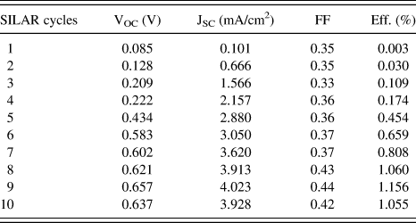
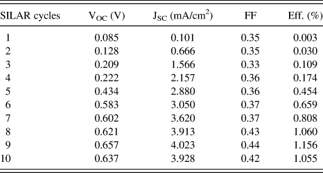
The CdS quantum dot-sensitized ZnO nanorod electrode was used as the photoelectrode in the thin sandwich-type cell with Pt-coated FTO as the counter electrode, a spacer film, and an electrolyte solution. CdS deposited onto ZnO by the SILAR method, and the deposition cycles range from 1 to 10. The resulting J-V curves are shown in Fig. 9, and the corresponding parameters are listed in Table I. It can be easily seen that as the SILAR deposition cycles increase (less than 9), values of the short-circuit current density (JSC), open-circuit voltage (VOC), fill factor (FF) and conversion efficiency (η) of CdS-sensitized solar cells all increase. But when the deposition cycles exceed 9, values of all the above parameters decrease. We fabricated five groups of solar cells totally; they all had the same trend. When the deposition cycles are 9, the conversion efficiency is 1.156%, it is the highest efficiency that the CdS-sensitized solar cells could achieve in terms of performance, the corresponding JSC was 4.023 mA/cm2, VOC was 0.657 V.
J-V curves of CdS-sensitized solar cells with different deposition cycles.

Parameters obtained from the J-V measurement of CdS-sensitized solar cells.
This can be explained as follows: when the deposition cycles increase from 1 to 9, more and more CdS are adsorbed on the surface of ZnO nanorods, they become much more compact and much more uniform, this morphology can produce more photogenerated carriers, and it contributes to electrons transport. Furthermore, when the grain size of CdS increases, the bottom of conduction band of CdS gets close to that of ZnO, and the contact between ZnO nanorods becomes relatively good, so that electrons transfer to the external circuit quickly and efficiently, resulting in the increase in JSC and FF. As the amount of photogenerated carriers increases, so the quasi-Fermi level of ZnO increases with the increases in density of the electrons injected from the CdS QDs into the ZnO conduction band, VOC increases accordingly under the illumination. Consequently, the photoelectric conversion efficiency of solar cells increases. However, when the deposition cycles exceed 9, the adsorbed CdS increase along the thickness direction, the aggregation of CdS QDs and bad coverage of the ZnO surface, the gap between ZnO nanorods decrease, it is difficult for electrolyte to cover the surface of ZnO, so the electrolyte does not maintain contact completely with CdS that are on the surface of ZnO. This causes an increase in the recombination probability of photogenerated electrons, so JSC, VOC and FF decrease, eventually, the photoelectric conversion efficiency of solar cells decreases.
Because we used simplified packaging, we measured the solar cell efficiency half an hour after injecting the electrolyte and accordingly, we have not tested the solar cell lifetime and stability. We will do this research in our subsequent work.
IV. CONCLUSION
In this article, we used TiCl4 pretreatmentReference Xu, Hu, Luo, Liu and Dai17 to grow a layer of TiO2 nanoparticles onto FTO. We prepared a smaller-particle seed layer prior to growing ZnO to obtain smaller diameter ZnO nanorods. ZnO nanostructure was grown by the hydrothermal method. Finally, we assembled CdS-sensitized solar cells. We discovered that when the deposition cycles increased from 1 to 10, the solar cells performance initially strengthened, then weakened. When the deposition cycle is 9, the conversion efficiency is 1.156%, it is the highest.
ACKNOWLEDGMENTS
This work was partially supported by Key Project of Beijing Natural Science Foundation (3131001), Key Project of Natural Science Foundation of China (91233201), Key Project of Beijing Education Committee Science & Technology Plan (KZ201211232040), State 863 Plan of MOST of China (2011AA050527), State Key Laboratory of Advanced technology for Materials Synthesis and Processing of Wuhan University of Technology (2012-KF-6), Beijing National Laboratory for Molecular Sciences (BNLMS2012-21), State Key Laboratory of Fine Chemicals of Dalian University of Technology (KF1016), State Key Laboratory of Multiphase Complex Systems of Institute of Process Engineering of CAS (MPCS-2011-D-09 and MPCS-2010-A-02), Key Lab of Photochemical Conversion and Optoelectronic Materials of TIPC of CAS (PCOM201111 and PCOM201211), Key Laboratory of Semiconductor Materials Science of Institute of Semiconductors of CAS (KLSMS-1101), State Key Laboratory of New Ceramic and Fine Processing of Tsinghua University (KF1210), Key Laboratory of Renewable Energy and Gas Hydrate of Chinese Academy of Sciences (2012-10), and Beijing Key Laboratory for sensor (KF20121077206).