I. INTRODUCTION
The functionality and reliability of film/substrate systems are strongly influenced by residual stresses. These residual stresses can result from many sources, such as the thermal mismatch between the film and substrate,Reference Hsueh1–Reference Fang and Wickert3 defects in the films (grain boundaries, dislocations, voids, and impurities) during the film deposition process,Reference Mayr and Samwer4–Reference Nix and Clemens6 lattice mismatch between two single crystal materials,Reference Zhang, Lee, Guido and Hsueh7 and the surface stress in the film.Reference Cammarata and Trimble8 The residual stresses in the film/substrate systems also depend on the materials properties of the constituents and the film deposition process. For example, the residual stresses of the sputtered Al films depend not only on the film thickness but also on the sputtering pressure, substrate bias, and substrate materials.Reference Pletea, Koch, Wendrock, Kaltofen and Schmidt9–Reference Lee, Kim, Lee, Chung, Cheong and Kim11 Different residual stresses may influence the film growth mode and the adatom mobility during different processing stages. Therefore, several theoretical models have been developed to analyze the residual stresses in the film/substrate systems using the mechanical equilibrium conditions.Reference Hsueh1, Reference Hsueh and Lee12–Reference Hsueh, Lee and Lin14
Various techniques have been developed to measure the residual stresses of the film/substrate system.Reference Tsang, Mooney, Dacol and Chu15–Reference McCarthy, Pei, Becker and Atteridge22 Among those techniques, the approach of microcantilever beam has been widely used.Reference Fang and Lo2, Reference Fang and Wickert3, Reference Fang and Wickert19–Reference McCarthy, Pei, Becker and Atteridge22 Furthermore, due to the superior mechanical properties and the convenience of integrating in microelectromechanical system processes,Reference Riley23 silicon nitride is a candidate to produce flexible microcantilever with a sharp tip for atomic force microscope (AFM).Reference Akamine, Barrett and Quate24–Reference Viani, Schäffer, Chand, Rief, Gaub and Hansma27 Gold or aluminum layer was generally deposited to increase the reflectivity of the silicon nitride microcantilevers.Reference Khan, Philip and Hess26, Reference Viani, Schäffer, Chand, Rief, Gaub and Hansma27 However, the residual stresses in the Al (or Au) and silicon nitride systems will inevitably influence the mechanical properties and reliabilities of the microcantilever systems. Hence, it prompted us to investigate the residual stresses in Al film deposited on silicon nitride at two deposition temperatures using the technique of microcantilever.
II. EXPERIMENTAL
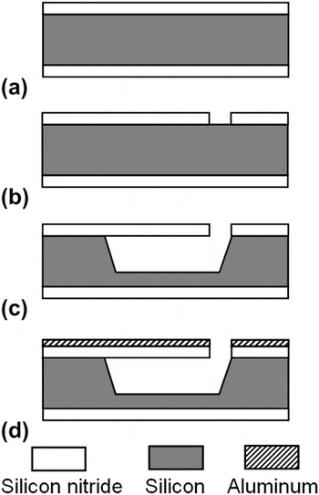
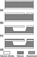
The schematic drawing of the processes to fabricate microcantilevers is shown in Fig. 1. Double-side polished 4″ Si wafers (Summit-Tech Resource Corp., Hsinchu, Taiwan) with (100) orientation and 550-μm thickness were used to carry out the conventional bulk micromachining. As shown in Fig. 1(a), silicon nitride (SixNy) film with 940 ± 28 nm thickness was firstly deposited on both sides of the wafer by low-pressure chemical vapor deposition (LPCVD; 400104-FUR, TYSTAR Corporation, Torrance, CA) with the reaction gas of 24 sccm dichlorosilane and 6.9 sccm ammonia. The deposition temperature and pressure were 875 °C and 0.1 Torr, respectively. Patterns of predetermined microcantilever beams with 100-μm length and 10-μm width were formed by lithography on one side of the SixNy coated wafer. After pattern transferred by dry etching and removal of the photoresists on the wafer [see Fig. 1(b)], wet etching with 45% (weight) KOH solution at 30 °C was used to remove the silicon underneath the SixNy microcantilevers as shown in Fig. 1(c). The samples with SixNy microcantilevers were finally rinsed by distilled water and then baked. The measurements of the thickness and the profile of microcantilevers were carried out by AFM (Dimension 3100; Digital Instrument Inc., Tonawanda, NY) and scanning electron microscope (SEM; JSM-6500F, JEOL Ltd., Tokyo, Japan). Elemental analyses of SixNy were performed by energy dispersive x-ray (EDX) spectroscopy using the JSM-6500F SEM with a Si/Li EDX detector. Finally, the Al film was deposited on the SixNy microcantilever as shown in Fig. 1(d).
Schematic of the fabrication process for microcantilever: (a) SixNy deposition on double-side polished 4″ Si wafer; (b) In-plane shape of the microcantilever defined and patterned on the SixNy film using the photolithography and dry etching processes; (c) KOH wet etching to remove the silicon underneath the SixNy microcantilever; and (d) Al evaporation on the SixNy microcantilever.

The deflections of microcantilevers were measured by WYKO interferometer (Veeco Instruments, Plainview, NY) before and after the deposition of Al films. The WYKO measurement was carried out at room temperature and at least five microcantilevers were measured per sampling interval. For Al film deposition, thermal evaporation with Al source (99.99% purity) was performed with the pressure of 5 × 10⁻⁶ Torr at 25 and 105 °C, respectively. The deposition temperature was controlled by the substrate water-cooling system and quartz heating lamp. The thickness and surface morphology of Al films were measured by AFM. From the deflection data, the residual stresses in the SixNy substrate and Al film were analyzed.
III. RESULTS AND DISCUSSION
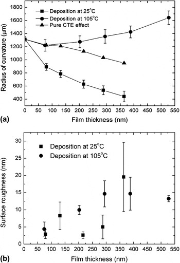
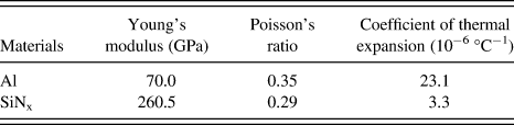
The profiles of microcantilevers were measured before and after Al deposition. Figure 2 shows the typical profile of an uncoated SixNy microcantilever measured by WYKO, where the radius of curvature of the uncoated SixNy microcantilever is 1313.7 ± 39.4 μm. The curvature of the uncoated SixNy microcantilever is due to the gradients of Si/N ratio and the atomic density in the direction of thickness.Reference Toivola, Thurn, Cook, Cibuzar and Roberts28–Reference Shi, Zhang, Zhang and Li30 EDX analysis of SixNy shows a nonfixed ratio of x to y, which indicates that the LPCVD silicon nitride herein is nonstoichiometric, i.e., SiNx.Reference Bouridah, Mansour, Beghoul, Mahamdi and Temple-Boyer31 For coated microcantilevers, the radius of curvature and surface roughness of microcantilevers as functions of Al film thickness are shown in Figs. 3(a) and 3(b), respectively. For the room-temperature-deposited microcantilevers, the radius of curvature decreases with increasing film thickness. However, for 105 °C deposition temperature, the radius of curvature increases with increasing film thickness when the film thickness is greater than 74 nm. The surface roughness (Ra) of the uncoated SiNx is 1.35 ± 0.06 nm, and the roughness after Al deposition is still in a good quality except for the one of the thickness of 364 nm deposited at room temperature. Using these deflections and the mechanical properties of Al and SiNx listed in Table I,Reference Khan, Philip and Hess26, Reference Chuang, Luger, Fettig and Ghodssi32, Reference Huang, Lou, Tsai, Wu and Lin33 the residual stresses in microcantilevers are analyzed as follows.
An uncoated silicon nitride microcantilever measured by WYKO interferometer shows an intrinsic deflection. Note that the flat plane on the right-hand side is the surface of the silicon nitride film on the silicon wafer.

(a) Radius of curvature of microcantilever and (b) surface roughness of the Al films as functions of Al film thickness.

Mechanical and thermal properties of Al and silicon nitride.

Stoney’s equation has been used extensively to characterize residual stresses in a thin film grown or deposited on a substrate, such thatReference Stoney34

where σst is the film stress (by Stoney’s equation), E, v and h are Young’s modulus, Poisson’s ratio, and thickness, respectively. The subscripts, s and f, denote the substrate and the film, respectively, and r is the radius of curvature of the bilayer system. Note that the curvature is positive when the film surface is concave. The term E/(1−v) denotes the biaxial modulus. However, it is worthwhile to point out that Stoney’s equation is valid only when the film has a negligible thickness compared to the substrate. When the film thickness is not negligible, Hsueh and LeeReference Hsueh and Lee12 proposed a method to solve the stress gradient through the thickness in an elastic bilayer arising from the bending curvature. The stresses in the substrate, σ s, and in the film, σ f, are


Note that B is the biaxial modulus and Δε is the unconstrained differential strain of the film with respect to the substrate. The total strain, ε, can be decomposed into the uniform strain c and the bending strain components, such that

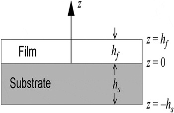
where z is the coordinate axis normal to film/substrate plane, the interface between the film and the substrate is located at z = 0 as shown in Fig. 4, and z = t b is the location of the bending axis corresponding to zero bending strain. Note that the second term on the right-hand side of Eq. (3) denotes the bending strain component. The solutions subjected to the force equilibrium and moment equilibrium conditions are


Schematics showing the cross section of a film/substrate system in modeling.

Equation (6) can be used to calculate the differential strain if the radius of curvature, biaxial modului, and thicknesses of films and substrates are given. Note that the curvature is positive when the film surface is convex for the present solution. Thus, the sign of curvature in the present solution is opposite to that in Stoney’s equation (e.g., the curvature shown in Fig. 2 is positive). The average film stress is defined by

Using Eqs. (3)–(6) and substituting Eq. (2b) into Eq. (7), the average film stress is

Considering the presence of curvature of the cantilever before film deposition, the effective curvature 1/r induced by the film deposition process and the mismatch between the film and the substrate is

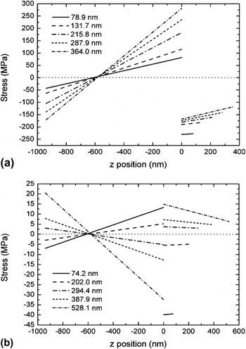
where 1/r A and 1/r B are the curvatures of microcantilever after and before film deposition, respectively. This effective curvature is used in Eqs. (1) and (6) to calculate the residual stresses. From the data shown in Fig. 3(a), the (effective) curvature 1/r is obtained. Then the differential strain Δε and total strain ε can be obtained from Eqs. (6) and (3), respectively. Using Eq. (2), the stress distributions in the Al film and SiNx substrate at 25 and 105 °C are shown in Figs. 5(a) and 5(b), respectively. For the Al film deposited at 25 °C, the stress in the Al film is always compressive regardless of the film thickness as shown in Fig. 5(a) and its magnitude at the free surface of the film is smaller than that at the film/substrate interface.
Stress distributions in substrates and Al films evaporated at (a) room temperature and (b) 105 °C.

Because thermal mismatch is excluded at room temperature deposition, the stresses in microcantilever originate from other sources such as dislocations or interfaces, etc. The stress in the SiNx substrate is (in-plane) compressive near the bottom free surface and tensile near the interface. However, for the Al film deposited at 105 °C, the stress in the Al film changes from compressive to tensile as the Al film thickness is greater than 294.4 nm [see Fig. 5(b)]. The stress state in the SiNx substrate also changes at the 294.4 nm film thickness. Such a change is due to the thermal mismatch between Al and SiNx and other sources. As seen in Table I, the coefficient of thermal expansion (CTE) of Al is larger than the CTE of SiNx. For pure thermal mismatch by cooling from 105 to 25 °C (ΔT = −80°C), the curvature induced by thermal mismatch can be calculated using Eq. (6) with Δε replaced by (αf − αs) ΔT, such thatReference Hsueh1, Reference Hu and Huang13, Reference Hsueh, Lee and Lin14

where α is the CTE. It is assumed in this study that other than the difference in thermal mismatch, the two systems deposited at room temperature and 105 °C have the same sources to produce the residual stresses. In this case, the curvature of the system with Al deposited at 105 °C can be obtained from that with Al deposited at 25 °C by simply adding the curvature induced by the thermal mismatch with ΔT = –80 °C. That is, the curvature shown by ▲ is the summation of curvatures shown by ▪ and induced by the thermal mismatch. The symbols • and ▪ stand for the experimental data of Al deposited at 105 and 25 °C, respectively. Comparing the values for symbols ▲ and •, the difference of radius of curvature increases with the film thickness. This is contradicting to the above assumption. It implies that the defects to produce the residual stresses in the system deposited at room temperature are different from those at 105 °C. The microstructures of microcantilever deposited at 25 and 105 °C will be studied in the near future.
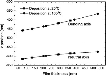
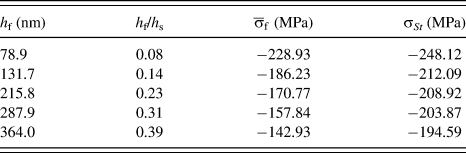
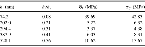
Using Eqs. (1) and (8), the average film stresses calculated from our experimental results are shown in Tables II and III. The average film stresses calculated by Stoney’s equation are always higher than the values calculated by the present solution regardless of the deposition temperature and film thickness. In addition, the thicker the film, the larger the difference is. For a thick film, the Stoney’s equation was corrected by the factor (1 + γδ 3)/(1 + δ), where γ designates the ratio of film biaxial modulus to substrate biaxial modulus and δ is the ratio of film thickness to substrate thickness.Reference Hsueh1, Reference Klein35 In this study, the correction factor is in the range from 0.92 to 0.67 for δ from 0.08 to 0.56. The results of Stoney’s equation after correction are the same as the values obtained from the present solution. The neutral axes and bending axes after Al deposition with different thicknesses are shown in Fig. 6. Both neutral axes and bending axes are located in the substrate and shift slightly toward the interface between Al film and SiNx substrate when the film thickness is increased. Note that there is no temperature effect on either neutral axes or bending axes because they are influenced by geometry, materials properties, and plastic deformation.
Bending axis and neutral axis as functions of Al film thickness.

The average residual stresses  and σSt (by Stoney) in Al film deposited at 25 °C.

The average residual stress  and σSt (by Stoney) in Al film deposited at 105 °C.

IV. CONCLUSIONS
The residual stresses in the Al/SiNx system measured by the microcantilever were investigated. Various thicknesses of Al films were deposited on SiNx microcantilevers by evaporation at 25 and 105 °C. For the room-temperature-deposited microcantilevers, the residual stress in the Al film was compressive and the microcantilever deflected toward the side of SiNx substrate. For the Al film deposited at 105 °C and when the thickness ratio of film to substrate was greater than 0.31, the residual stress in the Al film became tensile and the microcantilever deflected toward the side of Al film. The average film stresses calculated by Stoney’s equation were greater than those calculated by the present solution regardless of the deposition temperature and film thickness. Using the correction factor of (1 + γδ 3)/(1 + δ), the results of Stoney’s equation become the same as those obtained from the present solution. Both neutral axes and bending axes are located in the substrate and their positions vary with the film thickness, but they are independent of deposition temperature.
ACKNOWLEDGMENT
This work was performed under the auspices of the National Science Council, Taiwan.