I. INTRODUCTION
Increasing interest has been focused on one-dimensional (1D) nanostructures in recent years for their potential applications in nanoscale electronic devices,Reference Tans, Verschueren and Dekker1 optical devices,Reference Duan, Huang, Agarwal and Lieber2 and sensors.Reference Kong, Franklin, Zhou, Chapline, Peng, Cho and Dai3 Among 1D nanostructures, ZnO nanowires (NWs) have become an actively researched area because of their beneficial semiconductive properties (a wide band gap of 3.37 eV and large exciton-binding energy of 60 mV), easy synthesis,Reference Wang4, Reference Park, Choi, Siebein and Singh5 photocatalytic activity,Reference Huang, Mao, Feick, Yan, Wu, Kind, Weber, Russo and Yang6, Reference Xu, Yuan, Du, Ren, Bouvy, Halasa and Su7 and potential for integration into the sensor platform.Reference Comini, Faglia, Sberveglieri, Pan and Wang8, Reference Jeong, Oh, Nam, Kim and Myoung9 Grown with the vapor–liquid–solid (VLS) mechanism, the position and diameter of ZnO NWs are well controlled by the location and size of metal catalysts (especially Au).Reference Huang, Mao, Feick, Yan, Wu, Kind, Weber, Russo and Yang6, Reference Huang, Wu, Feick, Tran, Weber and Yang10–Reference Zhu, Chen, Gu, Warren and Osgood15 Recently, catalyst-free ZnO NWs have been developedReference Lee, Jeong and Myoung16–Reference Baxter and Aydil21 to simplify the fabrication process and eliminate potential contamination in semiconductor devices. ZnO islands or films formed first by physical deposition or chemical synthesis provide the nucleation area for the growth of 1D nanostructures.
The control of location, diameter, and length of NWs are critical for nanodevice fabrication. Several reports demonstrated the vertical growth of ZnO NWs on patterns of catalyst,Reference Huang, Mao, Feick, Yan, Wu, Kind, Weber, Russo and Yang6, Reference Huang, Wu, Feick, Tran, Weber and Yang10–Reference Fan, Fuhrmann, Scholz, Syrowatka, Dadgar, Krost and Zacharias13 and the spatial location of patterned catalyst determines the position of ZnO NWs, which is critical for applications such as light-emitting diodes and field emitters.Reference Huang, Mao, Feick, Yan, Wu, Kind, Weber, Russo and Yang6, Reference Park and Yi22, Reference Li, Lin, Lee and Tseng23 Lateral growth of ZnO NWs along a thin film pattern edge offers another approach to realize controlled lateral growth. Trench Au/Si electrodes were fabricated, and NWs grew from the sidewall of Au layer to bridge trenched electrodes.Reference Gao, Liu, Buchine, Weintraub, Wang and Lee24 ZnO patternsReference Law and Thong25, Reference Qin, Yang and Wang26 or nanoparticlesReference Lee, Islam and Kim27 have been deposited to realize the horizontal growth of those catalyst-free ZnO NWs on Si substrate.
In this work, we reported on selective lateral growth of ZnO NWs from the edge of Si/Al2O3/Si multilayer structure, which has potential to bridge patterned devices or for nanometer scale shadow lithography. Deposition conditions of controlled temperature and O2 pressure were found for catalyst-free ZnO growth on Al2O3 layer only (not on Si layer), which is critical for device integration. The two-stage growth of small NWs (∼10 nm in diameter) starting from pattern edge first followed by a secondary growth of base on the existing wire is observed. This mechanism differs from previous reportsReference Tang, Chang, Shan, Ma, Lui, Zapien, Lee and Lee28, Reference Pan, Budai, Dai, Liu, Paranthaman and Dai29 of NWs having a similar structure of the tip and base segments. Kinetics study demonstrates that the growth of the NWs was controlled by surface diffusion of Zn/ZnO precursor on the thin alumina face at optimal O2 pressures and growth temperatures.
II. EXPERIMENTAL DETAILS
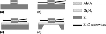
Patterned multilayer structures were deposited by sputtering, and ZnO NWs were grown by the chemical vapor deposition (CVD) in a two-zone tube furnace with Zn metal source. The fabrication process is shown in Fig. 1. Before sample preparation, the Si wafer (Silicon Quest International, Inc., San Jose, CA) was sequentially cleaned with acetone, isopropyl alcohol, deionized water, and nitrogen drying. Into a photoresist window (10 × 10 μm2 or 60 × 60 μm2), a multilayer of 20 nm of Si, 10 nm of Al2O3, and 20 nm of Si were sputtered, respectively, using an ATC 2000 sputtering system (AJA International, Inc., Scituate, MA) with a base pressure of 2 × 10⁻⁷ Torr. Lift-off process was carried out to result in square patterns of Si 20 nm/Al2O3 10 nm/Si 20 nm multilayer structures on Si wafer. The resulting 10-nm-thick alumina line at the pattern edge acts as the ZnO NW growth site as shown in Fig. 1 and is used to minimize the resulting ZnO NW diameter.
Schematic diagrams of ZnO nanowires (NWs) grown from the edge of SiO2/Si–Al2O3–SiO2/Si multistructure. (a) Sputtered Si/Al2O3/Si multilayer structure patterned by photolithography and liftoff, (b) ZnO NWs growing selectively from the pattern edge, (c) growth of ZnO NWs on Si/Si3N4 50-nm substrate, and (d) dimpling and etching of Si substrate to obtain the Si3N4 window transmission electron microscopy (TEM) sample.

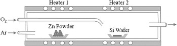
The growth of ZnO NWs was performed in a quartz tube furnace (2.5-cm inner diameter) by exposing patterned wafers to Zn vapor and O2 flow at 700 °C with a similar procedure as in Ref. Reference Park, Choi, Siebein and Singh5 (Fig. 2). Zn vapor pressure of ∼5 Torr, as measured by ZnO source weight loss and the known carrier gas volume flow rate at the growth temperature, was generated by heating zinc powder (98% purified; Mallinckrodt Baker LLC, Phillipsburg, NJ) to 600 °C. Patterned wafers were placed 8–10 cm downstream from the Zn source. At ambient pressure, a flow of 130 ± 2 sccm of Ar (99.998%; Scott-Gross Co., Inc., Lexington, KY) was used as the carrier gas when the heater was turned on. A separate O2 inlet (6-mm outer diameter) was placed 2 cm upstream from sample to prevent oxidation of Zn source. When the temperature of Si wafer reached 700 °C, a flow of 1.0 ± 0.03 sccm O2 (99.98%, Linde Gas LLC, Munich, Germany) was introduced to form ZnO NW. Both gas flows were controlled by the 1179A flow controllers (MKS Instruments, Andover, MA) and great care was taken to purge the chamber with an Ar flow to keep the metallic Zn source from being oxidized during heating. After reaching the designated reaction time, the growth of ZnO NWs was stopped by turning off the O2 flow and thermally quenching the system below growth temperature by opening the top-hinged heating elements of the tube furnace (>10 °C/s cooling rate).
Schematic illustration of the chemical vapor deposition (CVD) system used to grow ZnO NWs.

Scanning electron microscopy (SEM) images were characterized by Hitachi S900 (Hitachi, Tokyo, Japan) with field emission tip for nanometer resolution and Hitachi S3200 (Hitachi) equipped with high energy dispersive spectroscopy (EDS). High-resolution transmission electron microscopy (HRTEM) images were recorded by JEOL F2010 operated at 200 keV. Preparation of transmission electron microscopy (TEM) samples for ZnO NWs at the pattern edge required two steps as shown in Figs. 1(c) and 1(d). First, SiO2/Si–Al2O3–SiO2/Si patterns were deposited on the 50-nm-thick Si3N4 film covering the Si wafer, and ZnO NWs were grown using the same condition described earlier. Then, the backside of Si wafer was dimpled mechanically by the 656 dimple grinder (Gatan, Pleasanton, CA) and the residual Si was removed by a mixed acid (3HNO3:1HF:1HAc, volume ratio) to realize an electron transparent Si3N4 window under the patterned area.
III. RESULTS AND DISCUSSIONS
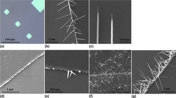
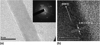
The optical image of SiO2/Si–Al2O3–SiO2/Si multilayer patterns is shown in Fig. 3(a). SEM shows that many ZnO NWs grow laterally from the pattern edge in Fig. 3(b), which is promising for integration between electrodes. These lateral NWs have another application as a shadow mask to form nanometer scale gaps in line of site depositions.Reference Chopra, Kichambare, Andrews and Hinds30–Reference Lefebvre, Radosavljevic and Johnson32 Each NW is composed of a tip segment with a diameter of ∼10 nm and a base segment with a diameter of ∼22 nm in Fig. 3(c). Previously, similar microstructures with larger diameter were reported in vertical growth processes.Reference Sekar, Kim, Umar and Hahn20, Reference Tang, Chang, Shan, Ma, Lui, Zapien, Lee and Lee28, Reference Pan, Budai, Dai, Liu, Paranthaman and Dai29 To prove that ZnO NWs were formed at pattern edges, a TEM study was used. Sample preparation required making an electron-transparent Si3N4 window underneath the patterned multilayer areas as shown in Fig. 1. Figure 4(a) shows a TEM image of a ZnO NW, and the selected area electron diffraction pattern in the inset indicates a single crystalline phase. The HRTEM image in Fig. 4(b) shows a spacing of 2.55 ± 0.07 Å between adjacent lattice planes corresponding to the distance between two (0002) crystal planes, confirming [0001] as the preferred growth direction (c-axis) for ZnO NWs.
(a) The optical image for patterns of SiO2/Si–Al2O3–SiO2/Si multilayer structure and scanning electron microscopy (SEM) images for (b) selective growth of ZnO NWs along the edge of patterns (10-nm Al2O3) with a reaction time of 30 min; (c) the tip segment and base segment; (d) Si patterns without Al2O3 layer after the same experimental process of (b); (e) low O2 flow (0.1 sccm) and (f) high O2 flow (>10 sccm); and (g) selective growth of ZnO NWs (20-nm Al2O3) with a reaction time of 30 min.

(a) TEM image and selected area electron diffraction pattern of a ZnO NW and (b) high-resolution transmission electron microscopy image of single crystalline ZnO NW with lattice fringes.

It is important to note that ZnO growth under these conditions was seen to come only from the pattern edge where the exposed Al2O3 layer resided and not on the Si layer, differing from the reported horizontal growth of ZnO NWs from Si substrates under different growth conditions.Reference Gao, Liu, Buchine, Weintraub, Wang and Lee24–Reference Lee, Islam and Kim27 Control experiments were applied to confirm that the selective growth was on Al2O3 and no defects were seen at the Si pattern edge. Samples of sputtered Si patterns on Si wafer were fabricated, and no wires were found growing along the edge of Si patterns (with native SiO2 coating) in Fig. 3(d). EDS analysis of those samples shows no Zn, indicating that no Zn particles or zinc silicide/silicate compounds form at the edge of Si patterns. The feed Zn source is at 600 °C and growth is at 700 °C, and so it is not expected for elemental Zn to condense on the sample surface, but will need to react with oxygen to form a nonvolatile surface species. The Al2O3 appears to act as a surface for this reaction while it does not occur on Si/SiO2 or on the growing ZnO wires under these conditions. To test this hypothesis, the exposed area of Al2O3 was doubled by producing a thicker SiO2/Si–Al2O3 20 nm–SiO2/Si multilayer structure followed by 30 min growth of ZnO at the same conditions. The ZnO volume density, calculated from NWs along the pattern edge with a scale of 1 μm, is ∼2.2 × 10⁻²⁰ m3, which nearly doubles the ZnO volume density by ∼1.0 × 10⁻²⁰ m3 of SiO2/Si–Al2O3 10 nm–SiO2/Si samples as in Fig. 3(b). It is important to note that the initial/tip diameter of ZnO NWs remained 10 nm and was not set by the thickness of the catalytic layer (20 nm) as had been seen in carbon nanotube (CNT) growth.Reference Chopra, Kichambare, Andrews and Hinds30
It is well known that well-aligned ZnO NWs can grow on sapphire substrateReference Huang, Mao, Feick, Yan, Wu, Kind, Weber, Russo and Yang6, Reference Fan, Fuhrmann, Scholz, Syrowatka, Dadgar, Krost and Zacharias13 and on high-quality alumina layers deposited by atomic layer deposition.Reference Hausmann, Becker, Wang and Gordon33–Reference Hu, Yao and Hinds37 In this work, amorphous Al2O3 thin films were deposited by sputtering, and ZnO subsequent NW growth is not as well aligned as growth from oriented crystal facets.
The CVD growth conditions are critical for the morphology control of ZnO NWs. The tip and base segments dominate NWs’ structures when a sufficient O2 is supplied (∼5 Torr partial pressure at a flow rate ∼1 sccm). No growth of ZnO NWs was found when the O2 flow was zero. A few conical-shaped NWs were found at the pattern edge with a low O2 pressure of ∼0.5 Torr, as shown in Fig. 3(e). When an excessive O2 is provided, for example, O2 pressure of ∼50 Torr, there is uncontrolled growth of ZnO and tetrapod-shaped NWs grow both on alumina and silicon as shown in Fig. 3(f). Similar structures had been reported in O2-rich concentrationReference Park, Choi, Siebein and Singh5, Reference Cha, Song, Jang, Jung, Han, Ha, Hong, Kang and Kim38–Reference Feng, Cheng, Lei, Wang and Loy41 during ZnO growth. Reaction temperature is another parameter affecting the growth of ZnO NWs. At growth temperatures of 675, 700, 725, and 800 °C and reaction time of 10 min, NWs with a length of 469 ± 54, 1118 ± 86, 778 ± 135, and 244 ± 41 nm, respectively, were obtained. Large ZnO particles appeared when samples were heated over 725 °C consuming Zn/ZnO source and resulting in short ZnO NWs at 800 °C.
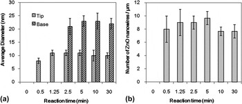
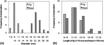
To study the growth mechanism, a kinetic study with samples of different reaction times (0, 0.5, 1.25, 2.5, 5, 10, and 30 min) was performed. All the diameter and length data are calculated statistically by 30 NWs selected randomly in each sample. Figure 5(a) shows the diameter variation of the tip and base segments grown in 30 min. With constant diameters of tip and base at 10 and 22 nm, respectively, Fig. 5(b) shows a constant linear density on Al2O3 surface along the pattern edge. The density is 8–10 NWs per micrometer. The summary of diameter and length distributions of ZnO NWs at 30 min is shown in Fig. 6. The diameters of tip and base are 10 ± 1 and 22 ± 2 nm, respectively, which are consistent with the data in Fig. 5(a). The length of base (1244 ± 175 nm) is one order longer than that of the tip (120 ± 20 nm) and dominates the total length of NWs. The small deviation of the diameter, length, and density data in Figs. 5 and 6 reveals a uniform growth of ZnO NWs along the exposed Al2O3 line between two Si layers, including a simultaneous nucleation and a similar growth rates for most ZnO NWs, allowing for a kinetic study at periodically interrupted times.
(a) Diameter of tip and base segments (30 samples observed) and (b) NWs’ densities as a function of CVD growth time.

(a) Diameter and (b) length distribution of tip and base segments with a reaction time of 30 min (30 samples observed for both charts).

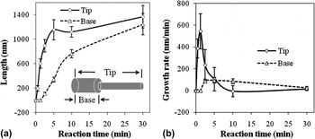
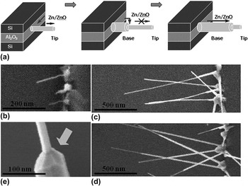
The length of ZnO NWs as a function of time is shown in Fig. 7(a). Growth rate versus reaction time [Fig. 7(b)] is derived from the slope at each time in Fig. 7(a). Ten nanometer diameter ZnO NW growth is initially fast but increases slowly after a 5-min reaction of Zn and O2. The growth rate of NWs at 1.25 min, also being the growth rate of tip segments at that time, reaches maximum at 543 nm/min, which is close to that of ZnO NWs having a surface diffusion–induced growth at 700 °C.Reference Kim, Gosele and Zacharias42, Reference Rackauskas, Nasibulin, Jiang, Tian, Statkute, Shandakov, Lipsanen and Kauppinen43 After this moment, base segments start to grow and stop the fast growth of tip segments as the base segments consume most of the ZnO source material before it diffuses to the tip segments. The lack of tip growth also shows that negligible Zn/ZnO intermediate surface species is formed on the ZnO NW surface in these growth conditions but requires the Al2O3 surface. If small, 10-nm-diameter, ZnO NWs are required, then growth time should be limited to less than 5 min.
(a) Length and (b) growth rate of the tip and base segments of ZnO NWs during the growth process. The solid and dash lines are drawn as guides for the eye.

Growth of ZnO NWs has been typically explained by the VLSReference Wagner and Ellis44 and vapor–solid (VS)Reference Brenner and Sears45 mechanisms. In this work, ZnO NWs grew by a VS growth mechanism owing to the absence of catalyst or liquidus sphere. The growth of ZnO NWs is limited by the formation of a surface ZnO intermediate and surface diffusion on the Al2O3 surface to the ZnO NW growth site at the NW tip or at the front of the basal regrowth.
Under these experimental conditions, the amount of Zn/ZnO material provided by Al2O3 layer should be constant for each NW. At the beginning of the tip growth,

and at the beginning of base growth,

So subtracting Eq. (1) from Eq. (2) and dividing common terms results in

where C is the concentration of Zn/ZnO on Al2O3 surface, d is the thickness of Al2O3 film, δ is the thickness of Zn/ZnO molecular layer, r t and r b are the diameter of tip and base segments, and l t and l b are the length of tip and base segments, respectively. The diffusion constant of Zn/ZnO on Al2O3 surface is considered constant and defined as  . As illustrated in Fig. 7(b),
 , the growth rate of tip segments before base growth, is 543 nm/min at 1.25 min;
 , the growth rate of tip segments after base growth, is 233 nm/min at 2.5 min; and dl b/dt, the growth rate of base segments, is 86 nm/min at 2.5 min. r t and r b are 10 and 22 nm, respectively. So the ratio of growth area of base segments to that of tip segments is (222 – 102)/102 = 3.8, and

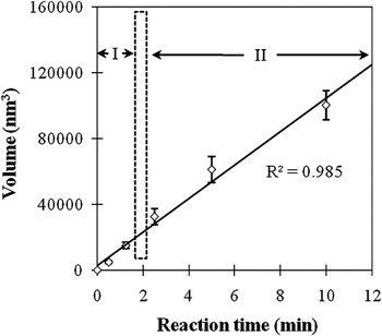
which is close to the experimentally observed  nm/min. It is important to note that Eq. (3) is a geometric argument that the volume growth rate of the secondary base (large diameter) would be equal to the initial tip (small diameter) volume growth rate if supplied a constant amount of Zn/ZnO to the NW base. Other growth mechanisms (direct VS growth on ZnO NW or at growth facets) would not give such a relationship. To further show this relationship, Fig. 8 shows a linear volume increase of ZnO NWs during the first 10 min of growth, where both tip and base growth occurs, which is consistent with the proposed growth mechanism.
Average ZnO NW crystal volume during the growth process on 10-nm-thick Al2O3 seed layer. ZnO NWs in region I have only the tip segment. ZnO NWs in region II have both the tip and base segments.

The proposed growth mechanism of ZnO NWs and corresponding SEM images are shown in Fig. 9. At the beginning of the reaction, Zn/ZnO precursor is formed on the thin Al2O3 layer nucleating 10-nm-diameter ZnO NW growth. The Zn/ZnO intermediate formed on Al2O3Reference Heo, Ip, Pearton, Norton and Budai46 diffuses along the ZnO NW to the growth plane at the tip of NWs to support a continuous growth, as shown in Fig. 9(b) at 0.5 min. Between 1.25 and 2.5 min, a secondary nucleation occurs at the base. Then, the base segment start to grow and consume Zn/ZnO source at the base surface, which nearly stops the further growth of tip segments [5 min in Fig. 9(c)]. Then, the base segments continue to grow and cover the initial narrow tip sections, reducing the observable tip length as seen in Fig. 9(d). Larger crystals having clear crystal facets [Fig. 9(e)] are assumed to have similar structure as the base facets. They appear at roots of the NWs and consume most of the Zn/ZnO material and cover the reactive Al2O3 area, thus reducing ZnO NW growth rate.
(a) Proposed growth mechanism of ZnO NWs and SEM images of ZnO NWs with a reaction time of (b) 0.5 min, (c) 5 min, and (d) 10 min; (e) SEM image of a large crystal grown at the base and assumed to be representative of the structure in Fig. 8(c).

IV. CONCLUSIONS
Lateral ZnO NWs have been successfully grown from the edge of SiO2/Si–Al2O3–SiO2/Si multilayer structure. Small, 10-nm-diameter, tip segments grow first followed by the growth of base segments (>20 nm), which stops the narrow tip growth. Kinetics studies show that this two-step growth is diffusion limited and a constant Zn/ZnO flux from the thin exposed Al2O3 layer. This leads to a faster growth rate of the tip segment compared to base segment rate but at a constant volume growth rate. The selective growth of NWs on alumina, without any growth on silicon, is an important step in the integration of ZnO NWs in patterned devices.
ACKNOWLEDGMENTS
The authors thank Dr. Janet K. Lumpp for providing the flow controller and Dr. John Balk for help in the fabrication of TEM samples. The authors thank the Air Force Office of Scientific Research, Defense Experimental Program to Stimulate Competitive Research (DEPSCoR) under agreement number F49620-02-1-0225, National Science Foundation CAREER (0348544), and National Science Foundation Nanoscale Interdisciplinary Research Teams (NSF NIRT) (0609064). Support was also provided by the Department of Chemical and Materials Engineering, Center for Nanoscale Science and Engineering, and Electron Microscopy Center in University of Kentucky.