I. INTRODUCTION
ZnO has great potential to be used as a material for optoelectronics components thanks to its suitable bandgap (∼3.4 eV) and high excitation binding energy (∼60 meV).Reference Meyer, Alves, Hofmann, Kriegseis, Forster, Bertram, Christen, Hoffmann, Straßburg, Dworzak, Haboeck and Rodina1–Reference Klingshirn, Meyer, Waag, Hoffmann and Geurts3 However, the difficulties encountered when attempting to dope ZnO p-type have slowed down the device development. One of the more promising group V dopants for obtaining p-type ZnO is nitrogen, as it should be easily incorporated on the O sublattice thanks to its similar size. Doping through both implantationReference Børseth, Tuomisto, Christensen, Monakhov, Svensson and Kuznetsov4–Reference Myers, Myers, General, Lee, Shao and Wang6 and incorporation during growthReference Lautenschlaeger, Eisermann, Meyer, Callison, Wagner and Hoffmann7–Reference Tarun, Zafar Iqbal and McCluskey9 are intensively investigated.
Positron annihilation spectroscopy is an effective method for the investigation of vacancy-type defects in semiconductors. Positrons implanted into a solid can get trapped in and localize at neutral and negative vacancies due to the missing positive ion core. This results in observable changes in the measurable annihilation characteristics, i.e., the positron lifetime and the momentum distribution of the annihilating positron–electron pair (Doppler broadening). In addition, positrons may have shallow hydrogenic states at negative ions, such as acceptor impurities. The annihilation data can be used to determine the vacancy concentration as well as to distinguish between different vacancy types and their chemical environment.
Vacancies in ZnO have been studied using positron annihilation spectroscopy by many research groups since the late 1980s, most of them dealing with bulk ZnO crystals and radiation damage.Reference Puff, Brunner, Mascher and Balogh10–Reference Chen, Wang, Maekawa, Kawasuso, Naramoto, Yuan and Sekiguchi12 In spite of the considerable research effort especially during the last 10 years, the understanding of many basic characteristics of the defects in ZnO is still quite limited. In particular, studies of doping effects on the vacancy defects structure are relatively scarce. In this paper, we present results obtained with positron annihilation spectroscopy in N-doped ZnO thin films and bulk crystals. We compare these new findings to those published earlier on N-implanted ZnO and discuss the special relationship between N impurities and vacancy clusters in the ZnO lattice.
II. EXPERIMENTAL DETAILS
A. Samples
The ZnO thin films with a thickness of 400–500 nm were grown by chemical vapor deposition (CVD) using metallic zinc, NO2, and NH3 as precursors. The nitrogen concentration was varied by adjusting the dopant flow between 20 and 100 sccm using a constant growth temperature of 350 °C. The low temperature was chosen to push the achievable nitrogen concentration into the 1020 per cm3 range as the solubility of nitrogen drastically decreases with increasing growth temperature.Reference Lautenschlaeger, Eisermann, Haas, Zolnowski, Hofmann, Laufer, Pinnisch, Meyer, Wagner, Reparaz, Callsen, Hoffmann, Chernikov, Chatterjee, Bornwasser and Koch8 All films were grown on nonpolar a-plane substrates since the incorporation of unintentional impurities during the CVD process is reduced by using either a-plane or c-plane Zn-face substrates as compared with O-face ZnO,Reference Lautenschlaeger, Sann, Volbers, Meyer, Hoffmann, Haboeck and Wagner13,Reference Wagner, Bartel, Kirste, Hoffmann, Sann, Lautenschläger, Meyer and Kisielowski14 and higher nitrogen doping levels can be achieved.Reference Lautenschlaeger, Eisermann, Meyer, Callison, Wagner and Hoffmann7,Reference Lautenschlaeger, Eisermann, Haas, Zolnowski, Hofmann, Laufer, Pinnisch, Meyer, Wagner, Reparaz, Callsen, Hoffmann, Chernikov, Chatterjee, Bornwasser and Koch8
Bulk ZnO samples were grown by seeded chemical vapor transport (CVT) using ammonia (NH3) as a source of nitrogen dopants.Reference Jokela and McCluskey15 ZnO and graphite powder were loaded into one end of a fused silica ampoule. A seed crystal16 was attached to the deposition end, ∼10 cm from the source powder. The ampoule was evacuated, backfilled with ½ atm NH3, and sealed using hydrogen–oxygen torch. The ampoule was placed in a three-zone horizontal furnace that maintains a temperature of 1000 °C at the source end and 880 °C at the deposition end.
B. Positron annihilation spectroscopy
In this work, the positron lifetimes in bulk crystals were measured using a conventional fast–fast coincidence spectrometer with a time resolution of 250 ps.Reference Saarinen, Hautojärvi, Corbel and Stavola17 Two identical sample pieces were sandwiched with a 20 μCi positron source (22Na deposited on 1.5-μm Al foil). Typically, 2 × 10⁶ annihilation events were collected in each positron lifetime spectrum. The lifetime spectrum n(t) = ΣiI iexp(−t/τi) was analyzed as the sum of exponential decay components convoluted with the Gaussian resolution function of the spectrometer after subtracting the constant background and annihilations in the source material (typically a few percent, for details, see Ref. Reference Tuomisto and Makkonen18) The positron in state i annihilates with a lifetime τi and an intensity I i. The state in question can be the delocalized state in the lattice or the localized state at a vacancy defect. The increase of the average lifetime τave = ΣiI i τi above the bulk lattice lifetime τB shows that vacancy defects are present in the material. This parameter is insensitive to the decomposition procedure, and even a change as small as 1 ps in its value can be reliably measured. In the case of one type of vacancy defect, with specific lifetime τV, the decomposition of the lifetime spectrum into two components τ1 and τ2 is straightforward to interpret. The second lifetime component τ2 = τV gives directly the vacancy-specific lifetime and the first lifetime component is τ1 = (τB−1 + κV)−1 < τB, where τB is the positron lifetime in the delocalized state in the lattice and τV is the positron trapping rate into the vacancy defects.
The temperature dependence of the average positron lifetime τave is analyzed with the model of trapping and escape rates of positrons.Reference Tuomisto and Makkonen18 In this model, the trapping coefficient μV to a neutral vacancy is independent of temperature and to a negatively charged vacancy, it varies as T −0.5. The trapping rate of positrons into the vacancies (concentration c V) is κ V = μVc V (μV = 3 × 1015 cm3/s for Zn vacancies in ZnO at 300 K). Positrons can get trapped also at hydrogen-like Rydberg states surrounding negative ion-type defects (shallow traps for positrons). The positron trapping rate at the Rydberg state μR varies also as T −0.5, which is the result predicted by the theory of transition from a free state to a bound state in a Coulomb potential.Reference Puska and Nieminen19
The positron annihilation characteristics were measured in thin epitaxial films by using a mono-energetic continuous positron beam. As lifetime experiments are not possible with a continuous beam, the Doppler broadening of the annihilation radiation was monitored as a function of the beam energy, providing a depth profile of the signal. The motion of the annihilating electron–positron pair causes a Doppler shift in the annihilation radiation ΔE = cp L/2, where p L is the longitudinal momentum component of the pair in the direction of the annihilation photon emission. This causes the broadening of the 511 keV annihilation line. The shape of the 511 keV peak gives thus the one-dimensional momentum distribution ρ(p L) of the annihilating electron–positron pairs. A Doppler shift of 1 keV corresponds to a momentum value of p L = 0.54 a.u.
The Doppler broadening can be experimentally measured using a Ge gamma ray detector with a good energy resolution. The typical resolution of a detector is around 1–1.5 keV at 500 keV. This is considerably compared with the total width of 2–3 keV of the annihilation peak, meaning that the experimental lineshape is strongly influenced by the detector resolution. Therefore, various shape parameters are used to characterize the 511 keV line. The low electron-momentum parameter S is defined as the ratio of the counts in the central region (typically, p L < 0.4 a.u.) of the annihilation line to the total number of the counts in the line. In the same way, the high electron-momentum parameter W is the fraction of the counts in the wing regions of the line (typically, p L > 1.5 a.u.). Due to their low momenta, valence electrons mainly contribute to the region of the S parameter. On the other hand, only core electrons have momentum values high enough to contribute to the W parameter. Therefore, S and W are sometimes called the valence and core annihilation parameters, respectively.
III. N-DOPED CVD-ZNO
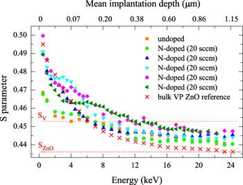
Figure 1 shows the S parameter measured at room temperature as a function of positron implantation energy in N-doped CVD-ZnO thin-film samples. When positrons are implanted close to the sample surface with E = 0–1 keV, a relatively high S parameter of up to S = 0.50 is recorded in the samples. These values characterize the defects and chemical nature of the near-surface region of the samples at the depth 0–5 nm. The region of constant S gives the characteristic value of the CVD-ZnO layer and extends up to 8 keV in the thickest sample. The decrease of the S parameter at higher implantation energies is due to the increasing fraction of positrons annihilating in the HT-ZnO substrate for which the characteristic S parameter is roughly S = 0.44, slightly above the value of the “defect-free” ZnO lattice.Reference Tuomisto, Ranki, Saarinen and Look11
S parameter as a function of positron implantation energy (probing depth) in CVD-grown ZnO:N thin films. The S parameters characterizing the ZnO lattice and the Zn vacancy are shown as dashed lines, determined based on the measurement data in the bulk VP ZnO (Ref. Reference Tuomisto, Ranki, Saarinen and Look11).

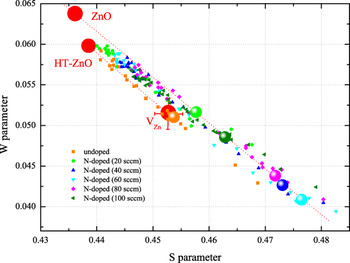
The S and W parameters measured in the N-doped CVD-ZnO layers are shown as plotted against each other with the positron implantation energy as running parameters in Fig. 2. The values characterizing the layers are highlighted in the figure. Figure 2 also shows the values of the ZnO lattice,Reference Tuomisto, Ranki, Saarinen and Look11 the isolated Zn vacancy,Reference Tuomisto, Saarinen, Look and Farlow20,Reference Zubiaga, Tuomisto, Coleman, Tan, Jagadish, Koike, Sasa, Inoue and Yano21 and those typical of HT-ZnO,Reference Johansen, Zubiaga, Makkonen, Tuomisto, Neuvonen, Knutsen, Monakhov, Kuznetsov and Svensson22,Reference Johansen, Zubiaga, Tuomisto, Monakhov, Kuznetsov and Svensson23 adjusted for the detector resolution, and geometry applied in these experiments. It is clearly seen that at high positron implantation energies, the measured data converge toward the HT-ZnO point as expected. Interestingly, the (S, W) point measured in the undoped CVD-ZnO sample coincides with the Zn vacancy point. This is interpreted as saturation trapping to single Zn vacancy-related defects, whose concentration hence needs to be above 5 × 10¹⁸ per cm3.Reference Zubiaga, Tuomisto, Coleman, Tan, Jagadish, Koike, Sasa, Inoue and Yano21 On the other hand, the (S, W) points characterizing the N-doped CVD-ZnO samples all fall on a line that goes through the ZnO lattice values (S B, W B) and runs to the right of the ZnO–V Zn line. This together with the relatively high S parameter values (S goes up to 1.09 × S B) indicates that the N-doped samples contain important concentrations of clusters of vacancies, containing both Zn and O vacancies (clusters of Zn vacancies only would be indistinguishable from single Zn vacanciesReference Rauch, Makkonen and Tuomisto24). Importantly, the linear behavior of the (S, W) parameters in the N-doped samples implies that the vacancy clusters have similar nature in all the samples and only their concentration changes.
(S, W) plot with positron implantation energy as the running parameter. The characteristic (S, W) points of the ZnO lattice, V Zn, and HT-ZnO (essentially LiZn) are shown for reference.

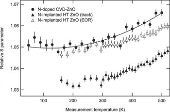
Figure 2 shows that the S parameter increases with N flow up to 60 sccm and then decreases again, indicating that the relationship between the N content and the concentration of the observed vacancy clusters is not straightforward. To determine the possible effect of negative ions on the room temperature data, we measured the N-doped ZnO samples at temperatures ranging from 40 to 500 K (data from a representative sample are shown in Fig. 3). The S parameter measured in the layer decreases with decreasing temperature, indicating that negative ions compete with vacancies in trapping positrons at low temperatures, as the negative ions produce the annihilation parameters of the defect-free lattice. The data are similar for all the N-doped samples; hence the differences in the S parameters measured at room temperature are due to differences in vacancy cluster contents rather than differences in negative ion introduction. It should be noted that the temperature dependence is very similar in N-implanted HT ZnO; also, vacancy clusters and negative ion-type defects have been observed.Reference Børseth, Tuomisto, Christensen, Monakhov, Svensson and Kuznetsov4
S parameter as a function of temperature in the 20-sccm ZnO:N thin film sample. The solid curve is drawn to guide the eye. Data from N-implanted HT ZnO are shown for comparison.

IV. N-DOPED CVT-ZNO
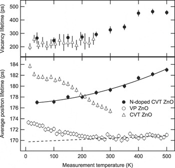
Figure 4 shows the average positron lifetime measured as a function of temperature in a bulk N-doped CVT-ZnO crystal as well as the second (vacancy) lifetime component extracted from the annihilation spectra. Results also from undoped CVTReference Tuomisto, Mycielski and Grasza25 and vapor-phase grown (VP) ZnOReference Tuomisto, Ranki, Saarinen and Look11 are shown for comparison. The increase of the average positron lifetime τave with decreasing temperature is a clear indication of the presence of negatively charged vacancy defects. In undoped VP ZnO, the monotonous behavior of the lifetime below 300 K indicates that these vacancy defects are the dominant negatively charged defect. On the other hand, in the undoped CVT ZnO sample, the slight change in the temperature dependence of the positron lifetime at 50–150 K is a sign of negative ion-type defects competing in trapping of positrons with the negative vacancies. This is observed also as the increase of the first lifetime component τ1 (not shown here) where the increased trapping in the negative ion-type defects brings the component closer to the bulk lifetime.
Average positron lifetime and the longer lifetime component as a function of measurement temperature measured in N-doped CVT ZnO. Data for undoped CVT ZnO and VP ZnO are shown for comparison. The solid curve is drawn to guide the eye, whereas the dashed line describes the effect of thermal expansion of the lattice on the ZnO lattice lifetime.

A longer lifetime component of τV = τ2 = 230 ± 10 ps can be extracted from the exponential lifetime spectra measured in the undoped CVT and VP samples below 300 K, whereas the data measured in the undoped ZnO sample above 300 K exhibit only one component. The longer lifetime component is constant as a function of temperature, implying that it represents positrons annihilation in one trapped state. This lifetime component is specific to the Zn vacancy. The lifetime τB = 170 ps is attributed o the annihilation from the delocalized state in the ZnO lattice at 300 K, whereas the slight increase of the average positron lifetime with temperature above 300 K in the undoped VP ZnO sample is due to thermal expansion.Reference Tuomisto, Ranki, Saarinen and Look11 The Zn vacancy concentrations in the undoped VP and CVT ZnO can be estimated to be 2 × 10¹⁵ per cm3 and 2 × 10¹⁶ per cm3, respectively.Reference Tuomisto, Ranki, Saarinen and Look11,Reference Tuomisto, Mycielski and Grasza25
The lifetime data obtained in the N-doped CVT ZnO are less straightforward to interpret. Vacancy defects are clearly present in this material, as the average positron lifetime is above the ZnO lattice lifetime (dashed line in Fig. 4). On the other hand, the decrease of the average positron lifetime with decreasing temperature is a sign of negative ion-type defects competing with the vacancies in positron trapping. Further, the vacancy lifetime component extracted from the lifetime spectra is quite long, about 450 ps, in particular at higher temperatures, whereas it decreases to below 300 ps at lower temperatures. The long lifetime of about 450 ps is indicative of the presence of large vacancy clusters where several Zn and O atoms are missing. The decrease of the vacancy lifetime component with decreasing temperature suggests that negatively charged Zn vacancies are present, too, and pull down the vacancy lifetime component when their attractiveness increases thanks to the T −1/2 dependence of the trapping coefficient. For this effect to be observable, the vacancy clusters need to be neutral. It should be noted that the decrease of the average positron lifetime with decreasing temperature cannot be explained by the Zn vacancies becoming more attractive, as this effect alone would increase the average positron lifetime.
V. DISCUSSION
The results obtained in N-doped thin-film CVD ZnO and N-doped bulk CVT ZnO crystals are very similar in nature: all the samples are found to contain relatively large vacancy clusters and negative ion-type defects, whereas positron data in undoped ZnO are usually dominated by a signal from defects related to single Zn vacancies. Earlier resultsReference Børseth, Tuomisto, Christensen, Monakhov, Svensson and Kuznetsov4 on N-implantation into ZnO are also quite similar. Already in the as-implanted samples, vacancy clusters are observed throughout the ion track and the projected range. Distinct evolution of the annihilation parameters is observed after the thermal treatments (furnace for 1 h) in the range of 600–1000 °C. After the highest temperature annealing (data in Fig. 3), N-implanted samples show vacancy clusters and negative ion-type defects. Hence, it seems that whenever N is present at important concentrations in the ZnO lattice, the material contains vacancy clusters and negative ions. It is natural to assign the latter to substitutional N impurities while the prevalence of vacancy clusters (instead of single Zn vacancy-related defects) is intriguing.
Earlier studies on ZnO show that defects related to single Zn vacancies are the main defects observed with positron annihilation spectroscopy. This is seen in both undoped and Al/Ga-doped thin filmsReference Zubiaga, Tuomisto, Coleman, Tan, Jagadish, Koike, Sasa, Inoue and Yano21,Reference Zubiaga, Tuomisto, Plazaola, Saarinen, Garcia, Rommeluere, Zuñiga-Pérez and Muñoz-San José26–Reference Look, Leedy, Vines, Svensson, Zubiaga, Tuomisto, Doutt and Brillson28 as well as in studies in bulk crystals.Reference Puff, Brunner, Mascher and Balogh10–Reference Chen, Wang, Maekawa, Kawasuso, Naramoto, Yuan and Sekiguchi12,Reference Johansen, Zubiaga, Makkonen, Tuomisto, Neuvonen, Knutsen, Monakhov, Kuznetsov and Svensson22,Reference Tuomisto, Mycielski and Grasza25 Clusters of vacancies in ZnO have been observed mainly in implantation studiesReference Børseth, Tuomisto, Christensen, Monakhov, Svensson and Kuznetsov4,Reference Johansen, Zubiaga, Tuomisto, Monakhov, Kuznetsov and Svensson23,Reference Chen, Maekawa, Yamamoto, Kawasuso, Yuan, Sekiguchi, Suzuki and Ohdaira29–Reference Neuvonen, Vines, Venkatachalapathy, Zubiaga, Tuomisto, Hallén, Svensson and Kuznetsov38 and also after heavy irradiation.Reference Zubiaga, Tuomisto, Coleman, Tan, Jagadish, Koike, Sasa, Inoue and Yano21 These vacancy clusters have been shown to disappear (become unstable) in thermal treatments at temperatures of about 800 °C, with a single exception: the N-implantation damage is stable up to at least 1000 °C in ZnO. Most of the implantation processing (with elements such as H, He, Li, N, O, and Si) has been performed on HT ZnO, i.e., material with a high concentration of Li that itself stabilizes the damage as observed in the electron irradiation experiments.Reference Puff, Brunner, Mascher and Balogh10,Reference Chen, Wang, Maekawa, Kawasuso, Naramoto, Yuan and Sekiguchi12 Hence, this cannot be the reason for the exceptional behavior of N implanted ZnO. A possible explanation could be that out of the so far implanted species, N could be the only one taking the substitutional position on the O sublattice. However, more work is clearly required to explain the mechanism of efficient implantation damage stabilization by nitrogen.
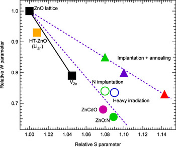
To illustrate the situation with N incorporation and the formation of various kinds of clustered vacancy defects in ZnO, data from a wide variety of ZnO samples are collected in Fig. 5. Samples where the dominant signal comes from Zn vacancies produce data that would fall on the line drawn between the “ZnO lattice” and “V Zn” points in the figure and are not shown.Reference Zubiaga, Tuomisto, Coleman, Tan, Jagadish, Koike, Sasa, Inoue and Yano21 ZnO bulk crystals grown by the hydrothermal method typically produce data that are close to the “HT ZnO” point (left to the ZnO–V Zn line) due to high concentrations of substitutional Li.Reference Johansen, Zubiaga, Makkonen, Tuomisto, Neuvonen, Knutsen, Monakhov, Kuznetsov and Svensson22 Implantation processing with elements other than N, followed by thermal treatments (furnace annealing at low temperatures or flash annealing at high temperatures), produce vacancy clusters that are characterized by the triangular symbols and the dashed line going through them and the ZnO point. These are clearly different in nature from the vacancy clusters introduced during the growth of N-doped ZnO or, e.g., ZnCdO,Reference Zubiaga, Plazaola, García, Reurings, Tuomisto, Kuznetsov, Egger, Zuñiga-Pérez and Muñoz-Sanjosé39 denoted by full circles. N implantation followed by annealing,Reference Børseth, Tuomisto, Christensen, Monakhov, Svensson and Kuznetsov4 as well as high-fluence particle irradiation,Reference Zubiaga, Tuomisto, Coleman, Tan, Jagadish, Koike, Sasa, Inoue and Yano21 produce vacancy clusters (open circles) that are rather similar to the in-grown vacancy clusters.
(S, W) plot with characteristic data from a variety of ZnO samples. The S and W parameters are shown as normalized to those of the ZnO lattice.

The high stability of the N-implantation induced and in-grown vacancy clusters in N-doped ZnO—the latter have survived the cooling down from relatively high growth temperatures—correlates with the similar nature observed in positron experiments. On the other hand, the vacancy clusters produced by implantation of other species than N—which disappear during high temperature anneals—are clearly different from the positron point of view. A possible reason is the balance between the amounts of Zn and O vacancies forming the clusters in question. A relatively simple idea, based on the positron data trends in another strongly cation–anion mismatched semiconductor InN,Reference Rauch, Makkonen and Tuomisto24 would be that the less stable clusters have more O vacancies. However, this interpretation is subject to more detailed studies (both experimental and computational) on the nature of multivacancy complexes in ZnO. Finally, an interesting observation that can be made is that in N-containing samples, similar to those presented here, Raman experiments show evidence of interstitial clusters.Reference Nickel40
VI. SUMMARY
We have studied N-doped CVD ZnO thin films and N-doped CVT bulk ZnO crystals with positron annihilation spectroscopy, with the aim of elucidating the role of nitrogen in the ZnO lattice. The positron methods are best suited for studying vacancy-type defects in semiconductors when the defect concentrations are above 1015 per cm3. A more general discussion of the results is made possible by the comparison with earlier results on a wide variety of undoped, doped, and implantation-processed ZnO samples.
We show that the introduction of N impurities into ZnO, irrespective of whether it is done during the growth of thin films or bulk crystals or through implantation and subsequent thermal treatments, leads to the formation of stable vacancy clusters and negative ion-type defects. The latter are quite likely the N impurities themselves (the concentrations have not been correlated) at substitutional positions. The existence of these vacancy clusters is observed almost exclusively for N introduction, whereas single Zn vacancy defects or easily removable vacancy clusters are more typically found in other cases. The close resemblance to effects observed in ZnO–CdO alloying suggests that formation of vacancy clusters in N-containing ZnO could be due to relaxation of stress/strain brought by the foreign species rather than electronic (Fermi-level) effects. The relation of the N-induced vacancy clusters with Zn interstitial complexes needs to be clarified.
ACKNOWLEDGMENTS
We wish to acknowledge the Academy of Finland for funding this research. Support by the DFG within SFB787 is acknowledged. Partial support was provided by the Department of Energy grant no. DE-FG02-07ER46386 (M.C.T.) and National Science Foundation grant no. DMR-1004804 (M.D.M.).