Introduction
New antenna designs with higher specifications are increasingly demanded so as to cope with modern communication devices requirements. One of the most important mechanisms that boost antenna performance aspects is the antenna reconfigurability. Antenna reconfigurability means that the antenna can adjust its operating frequency band, radiation pattern shape, and/or polarization, where different mechanisms are used to perform reconfigurability. Frequency reconfigurability of an antenna is its ability to operate in different frequency bands which is used to increase channel capacity, and switch between different wireless platforms [Reference Petosa1]. PIN switches are commonly used to switch between discrete frequency bands, while varactor diodes are commonly used to continuously tune the antenna to different frequency bands [Reference Tariq and Ghafouri-Shiraz2]. On the other hand, polarization reconfigurability is required for ciphering, increasing wireless system capacity, avoiding polarization mismatch, and eliminating multipath fading [Reference Gao, Sambell and Zhong3, Reference Valenzuela-Valdés, García-Fernández, Martínez-González and Sánchez-Hernández4]. Pattern reconfigurability saves energy by better directing signals toward intended transmitter, estimating angle of arrival, avoiding noisy environments, maneuver away from electronic jamming, and improving security [Reference Lin, Wong and Ziolkowski5–Reference Raman, Mohanan, Timmons and Morrison7].
Metamaterials are artificially engineered materials that add extraordinary properties to conventional materials, such as artificial magnetism, negative refractive index, negative permittivity and permeability [Reference Smith, Pendry and Wiltshire8]. Recently, metamaterials have been used to enhance antenna gain [Reference Attia, Yousefi, Bait-Suwailam, Boybay and Ramahi9], enhance antenna bandwidth [Reference Ha, Kwon, Lee and Choi10], electromagnetic coupling reduction in MIMO antennas [Reference Bait-Suwailam, Boybay and Ramahi11], and for filter design [Reference García-García, Bonache, Gil, Martín, Velazquez-Ahumada and Martel12]. Moreover, metasurfaces (MSs), which are 2D version of metamaterials, can be utilized to tune electromagnetic properties of dielectric substrates by either integrating electronic switches into them or by mechanically changing MS position with respect to dielectric substrates. This tunability in dielectric material properties leads to reconfigurable antenna response. Tunable MSs have been used to create frequency-reconfigurable [Reference Xu, Bi, Hao, Zhang, Xu, Dai, Xu and Zhou13–Reference Li, Kim, Luo, Li, Long and Sievenpiper17], pattern-reconfigurable [Reference Li, Zeng, Liu and Denidni18, Reference Luo, Kikuta, Han, Takahashi, Hirose and Toshiyoshi19], and polarization-reconfigurable antennas [Reference Ni, Chen, Zhang and Wu16, Reference Gao, Yang, Ma, Cheng, Yu and Cui20].
In [Reference Xu, Bi, Hao, Zhang, Xu, Dai, Xu and Zhou13], the authors proposed a frequency-reconfigurable radome that acts as a tunable bandpass shell for antenna systems in the X-Band. The tunability of the bandpass shell was attained by using complementary diamond-ring-shaped MS. By rotating the MS with certain angle from 0 to 90, electric field distribution changes and different modes are excited. The passband frequency changes from 11.0 to 9.4 GHz with low transmission losses. Also, the authors showed that this mechanism is simple as there is no need for an external control circuit or bias network to alter current distribution in the MS, and the structure of the complementary diamond-ring-shaped resonator is easy to fabricate. Another frequency-tunable metamaterial resonator was proposed in [Reference Nesimoglu and Sabah14] where S-shaped resonator, a ground frame, and a feeding transmission line are used to form a non-tunable resonator and then tunability is achieved by employing varactor diodes. By changing the reverse bias voltage from 0 to 14 V, the capacitances of the varactors are tuned from 2.22 to 0.33 pF and the resonance frequency also changes and linearly shifts. For instance, when the reverse voltage is 0 V, a resonance at around 1.25 GHz is achieved with nearly-unity transmission, and when the reverse voltage is 14 V, the resonance frequency shifts to around 1.85 GHz.
In [Reference Majumder, Krishnamoorthy, Mukherjee and Ray15], authors proposed frequency-reconfigurable antenna structure that consists of two MS layers fed by a linearly polarized slot antenna. Each MS layer consists of a periodic arrangement of I-shaped metallic patches placed in both the horizontal and vertical directions. By mechanically rotating the two MS layers with respect to the center of the slot antenna, the MS layers change the effective permittivity of the dielectric substrate. Consequently, the loading on the slot antenna and the operating frequency of the reported structure change. The operating frequency can be tuned from 2.55 to 3.45 GHz with a fractional tuning range of around 28%. The antenna provides a minimum gain of 5.3 dB with the peak gain being 8.3 dB.
In this paper, we propose a frequency-reconfigurable antenna structure consisting of a dielectric resonator (DR) topped by a superstrate material. Two MSs are placed upon the DR and the superstrate, where these two MSs are utilized to synthesize a localized reduction of the dielectric constant of the DR. By placing switches over one MS, the dielectric constant of the DR can be switchably synthesized to one of two predefined distributions, which is equivalent to switching the DR length to two different lengths. Consequently, the resonance frequency of the DR is tuned to two operating bandwidths. For the authors’ best knowledge, this is the first proposed MS-based turnable-frequency antenna that employs only on/off switches instead of using varactors/transistors/rotators as in previous works [Reference Xu, Bi, Hao, Zhang, Xu, Dai, Xu and Zhou13–Reference Li, Kim, Luo, Li, Long and Sievenpiper17]. The excited modes inside the proposed antenna were analyzed analytically and through simulation in each dielectric constant distribution of the DR. Also, the reduction in dielectric constant of the DR due to MS is analyzed through simulation. The proposed structure is fabricated and measured, and good agreement between measured and simulated results is attained. The antenna bandwidths are 1.1 GHz (14.7%) and 0.7 GHz (8%) and the gains are 5.1 and 7.8 dB, in the cases of having switches off and on, respectively.
The structure of this paper is organized as follows. In section “Proposed antenna”, we present an antenna ANT-I that is able to switch the distribution of dielectric constant of the DR to one of two predefined distributions, which is equivalent to switching the DR length to two different lengths. In section “Modified proposed antenna with less switches”, we discuss a modified antenna ANT-II that is similar to ANT-I but with relatively smaller number of switches. Finally, we discuss the fabrication and measurements of the proposed ANT-II in section “Simulation and experimental results” and we conclude our work in section “Conclusion”.
Proposed antenna
Antenna geometry
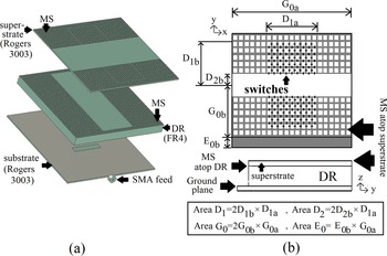
The proposed antenna is referred to as ANT-I, and it consists of three main parts as shown in Fig. 1(a). The first part is a feeding microstrip antenna that couples the input power to the DR through a slot in the ground plane, where the ground plane area is G 0 + E 0 as depicted in Fig. 1(b). The microstrip antenna is made using a Rogers 3003 substrate with ε = 3 and a height of 0.76 mm. The second part of the proposed structure is the DR that is made using FR4 material with ε = 4.4 and a height of 6.8 mm, where the top metal of the DR is perforated to form an MS. The design of this MS is discussed in the next section. The third part is a superstrate that is made using a Rogers 3003 substrate with ε = 3 and a height of 0.76 mm, where another MS is placed upon the superstrate with several integrated switches as will be discussed in the next subsection.
(a) Exposed view of the proposed antenna structure. (b) Antenna geometry of the proposed antenna.

Antenna analysis
In the antenna ANT-I, the MS atop the DR consists of a metal surface with square-perforations, where this MS covers the area G 0 − D 1. This uniformly-perforated MS can be utilized to reduce the effective permittivity of the underneath substrate to unity. To calculate the dielectric constant of the DR, we use a systematic method described in [Reference Smith, Schultz, Markoš and Soukoulis21] to retrieve the effective permittivity from reflection and transmission coefficients. In the aforementioned systematic method, we calculate


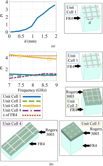
where t is dielectric slab thickness, $X = 0.5S_{21}^{-1}( 1-S_{11}^2 + S_{21}^2)$ , and the effective permittivity is ε eff = n/Z. As noted from Fig. 2(a), when the area of each square perforation equals 1 mm, the effective dielectric constant of DR reduces to unity. Thus, the dielectric constant value of the DR over the area G 0 − D 1 reduces to unity. Furthermore, when switches of the MS atop superstrate are closed, a square-perforated MS is formed over the area D 1 − D 2. Again, the same systematic method described in [Reference Smith, Schultz, Markoš and Soukoulis21] is used to calculate the dielectric constant value in the area D 1 − D 2. As depicted in Fig. 2(b) (Unit Cell 2), the dielectric constant value in the area D 1 − D 2 reduces to unity.
(a) Effect of d dimension increase on effective permittivity for unit cell 1, (b) Effective permittivity for MSs consisting of different unit cells.

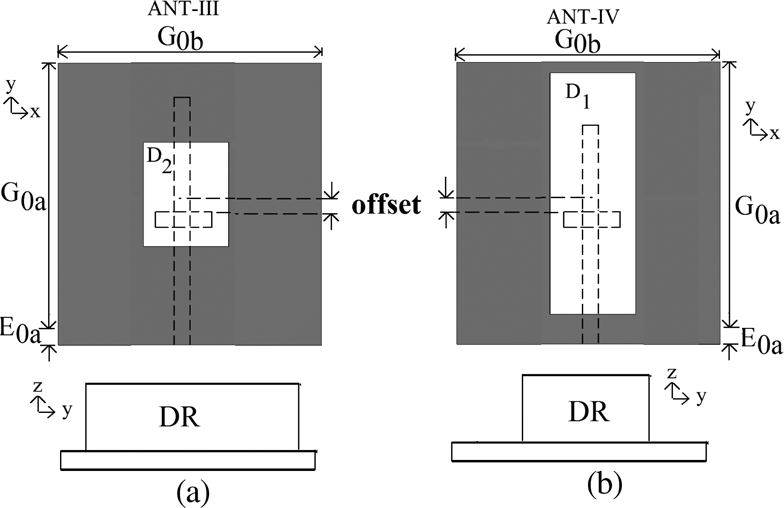
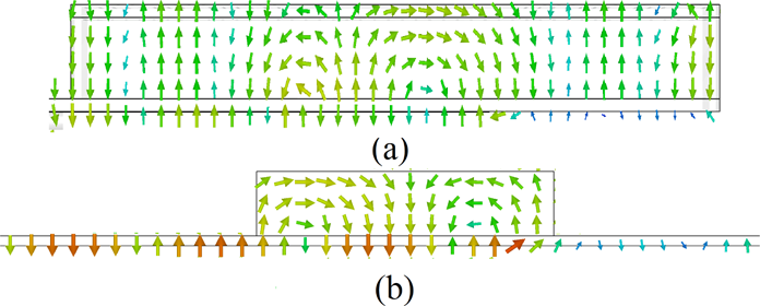
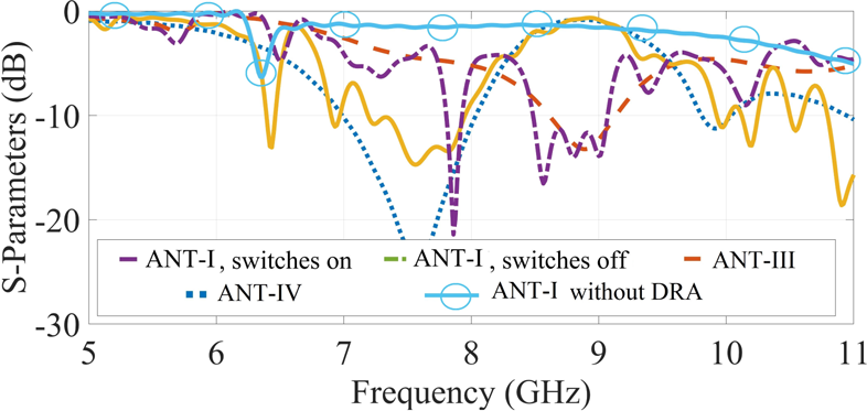
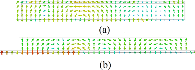
Consequently, the dielectric constant value of DR over the areas G 0 − D 1 and D 1 − D 2 reduces to unity. Thus, ANT-I with closed switches is assumed to be equivalent to a simple DR antenna, where the dielectric material only exists in D 2, namely ANT-III, as given in Fig. 3(b). To prove this assumption, the resonant modes excited inside each of ANT-I with closed switches and ANT-III are obtained using the characteristic mode analysis in the commercial software CST. The mode TE 21 is found to be excited in both antennas, where as we show in Fig. 4 the filed distribution of the mode TE 21 is excited in both antennas, noting that the field distributions are similar to each other. Moreover, we simulate and compare the responses of ANT-I with closed switches and ANT-III, as given in Fig. 5. Again, similar responses are attained indicating that both antennas are equivalent.
Dimensions in the xy plane (in mm): DR dimensions of ANT-III 21.1×21.9 (area D 2) and DR dimensions of ANT-IV 21.1×58.4 (area D 1); ground plane dimensions 56.6×60.6 (area G 0 + E 0); slot dimensions 16.6×3.3; offset 5.6; microstrip line of ANT-IV 3.3×45.8; microstrip line of ANT-III 3.3×40.5.

Field distribution of mode TE 21 at 8.5 GHz inside (a) ANT-I with switches turned on, and (b) ANT-III.

S-parameter simulation for proposed antenna ANT-I in cases of switches turned on and off.

Furthermore, the resonant modes excited inside a rectangular DR can be theoretically obtained using the waveguide model used by [Reference Mongia and Ittipiboon22]. In the aforementioned model, the resonance frequencies of $TE^x_{\delta np}$ mode are found by obtaining the zeros of the following function

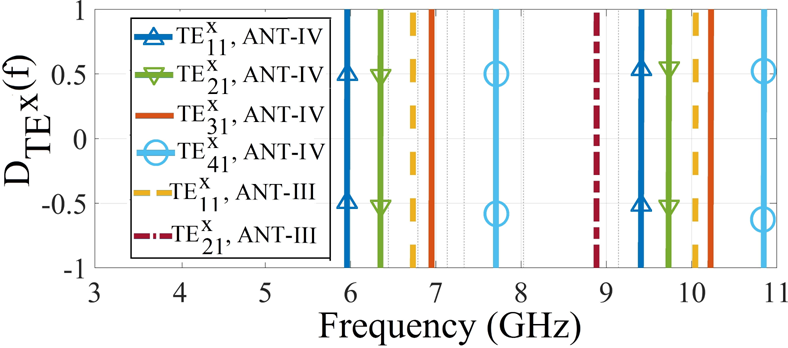
where $k^{2}_0 = ( k^{2}_x + k^{2}_y + k^{2}_z) /\epsilon$ , k x = δπ/d, k y = nπ/w, k z = pπ/b; d, w, and b are the DR dimensions in the x, y, and z directions, respectively; n and p are positive integers, and δ is a positive fraction of unity. We plot $D_{TE^x}( f)$
 for ANT-III in Fig. 6, where every zero-crossing represents DR resonance. As noted, multiple modes could be theoretically excited in the DR at different frequencies, but actual excited modes depend on the feeding mechanism. Only the modes whose field distributions fit with feeding structure field distributions can be excited. From Fig. 6, it is noted that mode TE 21 is excited in ANT-III at 8.9 GHz, which is a close resonance frequency obtained from CST simulation (8.5 GHz).
Plot of D function for ANT-IV and ANT-III.

On the other hand, turning the switches of the MS atop the superstrate off disrupts the distribution of square-perforated MS atop the superstrate in the area D 1 − D 2. The dielectric constant value resulting from this disrupted MS distribution is calculated using the same method described in [Reference Smith, Schultz, Markoš and Soukoulis21], and it is found that ε eff = 4.3 as shown in Fig. 2(b) (Unit Cell 3). Thus, ANT-I with open switches is assumed to be equivalent to a simple DR antenna, where the dielectric material only exists in D 1, namely ANT-IV, as given in Fig. 3(a). Again, the fields of ANT-I with open switches and ANT-IV are given in Fig. 7, where it shows the excitation of TE 41 in both antennas. Also, simulation results of ANT-I with open switches and ANT-IV are compared and presented in Fig. 5, where the similar responses of the two antennas indicate that they are equivalent to each other. Furthermore, the resonance frequency of the mode TE 41 can be theoretically obtained from Eq. (3) as given in Fig. 6. The mode TE 41 is found to be resonating at 7.7 GHz, which is close to the resonance frequency obtained from CST (7.2 GHz).
Field distribution of mode TE 41 at 7.5 GHz inside (a) ANT-I with switches turned off, and (b) ANT-IV.

Finally, we show in Fig. 5, the S-Parameter response for ANT-I without placing the DR element, the superstrate, and other MSs. It can be noted that antenna resonances completely vanish, indicating that the DR element, the superstrate, and other MSs have the main responsibility for exciting different modes inside the proposed antenna.
Modified proposed antenna with less switches
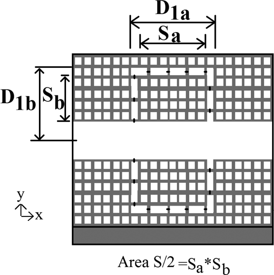
In the previous subsection, we proposed ANT-I that is able to switchably alter dielectric constant distribution of DR, so as to attain equivalent response to ANT-IV or ANT-III. However, the number of operating switches is large (see Fig. 1(b)), inspiring a modified proposed antenna with less number of switches and less consumed power. Thus, we propose a modified antenna ANT-II that is similar to ANT-I but with many switches replaced by short-circuits, as presented in Fig. 8.
Modified proposed antenna ANT-II with reduced number of switches in the MS atop superstrate.

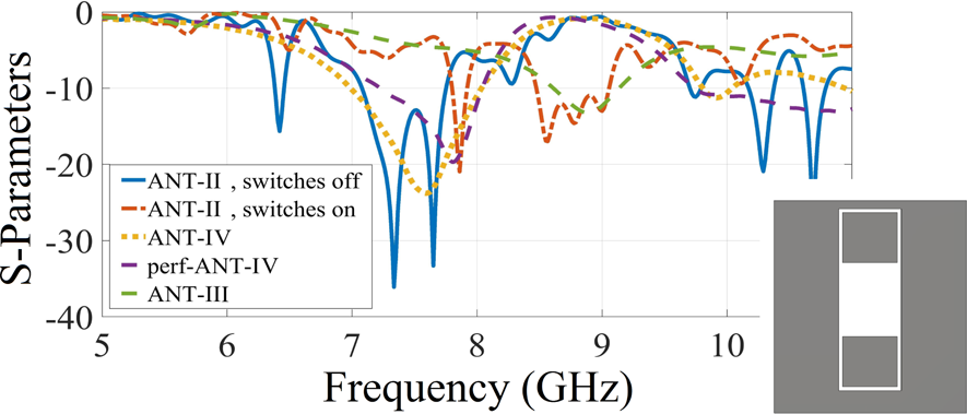
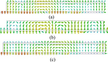
In the proposed antenna ANT-II with switches open, the MS atop the superstrate covers the area S and the MS atop the DR covers the area G 0 − D 1, wherein the dielectric constant of the DR is reduced to unity. This suggests that the proposed antenna is equivalent to a perforated/air-filled DR (perforated-ANT-IV) shown in Fig. 9. Using the characteristic mode analysis in CST, it is found that the mode generated in both ANT-II with open switches and perforated-ANT-IV is TE 41 as presented in (Fig. 10(a) and (b)). Also, by simulating S-parameter response for ANT-II with open switches and perforated-ANT-IV, and then comparing responses, similar results are obtained as in Fig. 9, indicating that the two antennas are equivalent.
S-parameter simulation for proposed antenna ANT-II in cases of switches turned on and off. Inset: ANT-IV with dielectric perforation in area S.

(a) Field distribution inside ANT-II with switches turned off. (b) Field distribution inside perf-ANT-IV. (c) Field distribution inside ANT-II with switches turned on.

On the other hand, for ANT-II, when switches atop superstrate are turned on, they form a rectangle-perforated MS over the small area D 1 − D 2 − S. Using the same method in [Reference Smith, Schultz, Markoš and Soukoulis21], the dielectric constant value is still close to unity, as given in Fig. 2(b). As the area D 1 − D 2 − S is small with dielectric constant value of DR close to unity, the antenna ANT-II with closed switches can be considered to be an equivalent to ANT-III. To verify that, we simulate the fields in ANT-II with closed switches and show the results in Fig. 10(c), where mode TE 21 is excited similarly to ANT-III. Further, we compare the simulation results of ANT-II with closed switches and ANT-III, and then show the results in Fig. 9. Similar obtained responses of both antennas indicate that they are equivalent to each other.
Simulation and experimental results
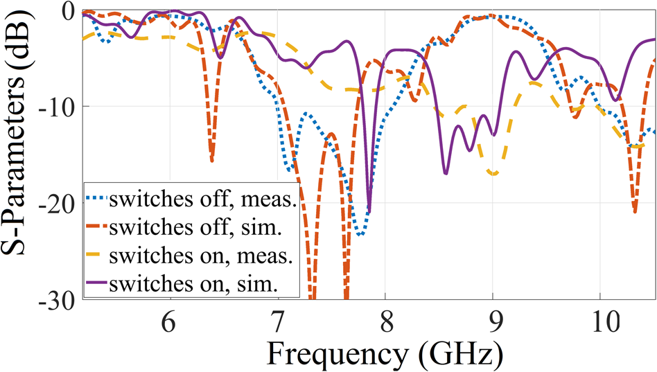
We fabricated two prototypes of the proposed antenna ANT-II as presented in Fig. 11. In one prototype, we replaced the switches of ANT-II by simple open-circuits which serve as turned-off switches, as shown in Fig. 11(a). In the second prototype, we replaced the switches of ANT-II by simple short-circuits which serve as turned-on switches, as shown in Fig. 11(b). Simulated and measured results of S-parameters are given in Fig. 12. The simulated bandwidths are 7.1–7.8 GHz (10.8%) and 8.5–9.1 GHz (6.9%) in cases of switches off and on, respectively; and measured bandwidths are 7–8.1 GHz (14.7%) and 8.5–9.2 GHz (8%) in cases of switches off and on, respectively.
Prototype of ANT-II with (a) open-circuits replacing turned-off switches, and with (b) short-circuits replacing turned-on switches.

Simulated and measured S 11 for ANT-II with switches turned on and off.

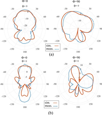
The radiation pattern for the antenna is also simulated, measured, and shown in Fig. 13. The simulated gains are 6.8 and 10 dB in cases of switches off and on, respectively; and the measured gains are 5.1 and 7.8 dB in cases of switches off and on, respectively.
Gain pattern of ANT-II at two cut angles in cases of switches tuned (a) off (7.2 GHz) and (b) on (8.7 GHz).

Conclusion
We proposed a frequency-reconfigurable DR antenna in this paper. The proposed antenna consists of a DR topped by an MS and fed by a microstrip antenna that couples power to a ground aperture. A superstrate topped by another MS was placed atop the DR, where switches are integrated into the MS of the superstrate to switch the dielectric constant distribution of the DR to one of two predefined distributions. The antenna was fabricated and measured, where the attained bandwidth of the proposed antenna was 1.1 GHz (14.7%) and 0.7 GHz (8%) in the cases of having switches off and on, respectively. Also, the gains of antenna are 5.1 and 7.8 dB in the cases of having switches off and on, respectively. The excited modes inside the proposed antenna were also analyzed analytically and through simulations.
 Ahmad Abdalrazik received his B.Sc. and M.Sc. degrees in Electrical Engineering from Port Said University, Egypt in 2012 and 2016, respectively. He received his Ph.D. degree from Egypt-Japan University of Science and Technology, Alexandria, Egypt, in 2020. He worked as a researcher at Kyushu University, Japan in 2019. Currently, he is an Assistant Professor at Port Said University. His research interests include antenna design, microwave devices, wave propagation modeling, metamaterial, and optimization.
 Adel B. Abdel-Rahman is currently a Professor at the Department of Electronics and Communications Engineering, Egypt-Japan University of Science and Technology, Alexandria, Egypt. He received his B.S. and M.S. degrees in Electrical Engineering, Communication, and Electronics from Assiut University, Egypt, and his Dr.-Ing. degree in Communication Engineering from Otto von Guericke University, Germany in 2005. Since October 2006, he has been an Assistant Professor at the Electrical Engineering Department, South Valley University, Qena, Egypt. He has published more than 120 refereed journal and conference papers and has two patents. He was the Executive Director for Information and Communication Technology, South Valley University, from 2010 to 2012. Since October 2012, he joined the School of Electronics, Communications and Computer Engineering, Egypt-Japan University of Science and Technology (E-JUST), Alexandria, Egypt, and has been the Dean of the Faculty of Computers and Information, South Valley University from 2016 to 2018. His research interests include the design and analysis of antennas, filters, millimeterwave devices, WPT, and metamaterials and their application in wireless communication, as well as optimization techniques with applications to microwave devices and antenna arrays.
 Ahmed Allam is currently an Associate Professor at the Department of Electronics and Communications Engineering, Egypt-Japan University of Science and Technology, Alexandria, Egypt. He received his B.Sc. degree in Electrical Engineering from Alexandria University, Egypt, and his M.Eng. and Ph.D. degrees from the University of Alberta, Canada. From April 1994 to January 1998, he worked as an Instrument Engineer with Schlumberger. From May 2000 to September 2001, he was with Murandi Communications Ltd., Calgary, Alberta, where he worked on RF transceivers design. From April 2007 to April 2008, he worked on RF CMOS transceivers design at Scanimetrics Inc., Edmonton, Alberta. His research interests include the design of RF circuits and systems.
 Mohammed Abo-Zahhad received the B.S.E.E. and M.S.E.E degrees in electrical engineering from Assiut University (AU), Egypt, in 1979 and 1983, respectively, and the Ph.D. degree from the University of Kent, Canterbury, UK, and AU (channel system), in 1988. He was promoted to an Associate Professor and a Professor of Electronics and Communication Engineering, in December 1993 and January 1999, respectively. He has also been a Professor of Electronics and Communication Engineering, since January 1999, the Dean of the School of Electronics, Communication and Computer Engineering, a Professor of Communication and Electronics Engineering with the Egypt-Japan University of Science and Technology (E-JUST), since January 2017. He was elected as the Vice-Dean for graduated studies, from August 2006 to June 2012, and the Chair of the Electrical and Electronics Department, from November 2013 to December 2016, both in the Faculty of Engineering, AU. In April 2018, he was selected by the Ministry of Higher Education as an expert for setting the study plans and regulations for new constructed universities in Egypt. He is currently the General Director of the E-JUST Information and Communication Technology Center. His research interests include switched-capacitor, optical and digital filters, biomedical and genomic signal processing, speech processing, data compression, wavelet-transforms, genetic algorithms, immune algorithms, wireless sensor networks, and electronic systems. He has published more than 160 articles in national and international journals and conferences in the above fields. He is a member of the European Society of Circuit Theory and Applications, in 1998. He has been a consultant of the Management Information Systems, Project Management Unit (PMU), Ministry of Higher Education, a member of the National Communication and Electronics Promotion Committee, as well as a Reviewer of the National Quality Assurance and Accreditation Authority, NAQQA, Egypt, since 2011.
 Kuniaki Yoshitomi received the B.S. and M.S. degrees in Electronics and D.E. degree in Communication Engineering from Kyushu University, Fukuoka, Japan, in 1979, 1981, and 1986, respectively, where he joined the Faculty of Engineering, in 1981. From 1990 to 1991, he was with the Department of Electrical Engineering, University of Washington, Seattle, WA, USA, as a Visiting Associate Professor. He is currently a Professor with the Center for Japan–Egypt Cooperation in Science and Technology, Kyushu University. His current research interests include antennas, scattering and diffraction, inverse problem, and electromagnetic compatibility.
 Ramesh K. Pokharel received the M.E. and Ph.D. degrees in Electrical Engineering from The University of Tokyo, Japan, in 2000 and 2003, respectively. He was a Post-Doctoral Research Fellow with the Department of Electrical Engineering and Electronics, Aoyama Gakuin University, Japan, from April 2003 to March 2005. In April 2005, he joined the Department of Electronics, Graduate School of Information Science and Electrical Engineering, Kyushu University, where he has been a Professor since October 2010. He served as the Deputy-Director of the Center for Egypt-Japan Cooperation in Science and Technology, Kyushu University, from April 2012 to March 2014, where he was the Director from April 2014 to March 2017. He has been a Visiting Professor with the Department of Electrical and Computer Engineering, Toronto University, Canada, since September 2019. His current research interests include the low-cost RFIC and analog circuits for microwave and millimeter wave wireless communications, on-chip signal integrity issues, on-chip meta-materials in CMOS, and near-field wireless power transfer system through human tissues. He was a recipient of the Monbu-Kagakusho (MEXT) Scholarship of the Japanese Government from 1997 to 2003, an excellent Center of Excellence (COE) research award from The University of Tokyo in 2003, and the 2016 Best ELEX Paper Award from IEICE, Japan. The students he has supervised have received five best presentation awards from different symposia/conferences. He served as the Secretary of the IEEE MTT-S Japan Society from January 2012 to December 2013 and as the Vice-Chair of Education Committee of IEEE-MTT-S Japan Society from January 2014 to December 2016, where he served as the Chair from January 2017 to December 2018 (based on document published on 16 January 2020).