I. INTRODUCTION
Bismuth telluride alloys have the highest thermoelectric (TE) figure of merit (ZT) near-room temperature for a commercially available bulk material.Reference Snyder and Toberer1 It is the preferred choice for cooler and generator applications with mean temperatures up to 200 °C when lead telluride and the TAGS alloy (GeTe)0.85(AgSbTe2)0.15 become a more efficient option. Legs with long length-to-area aspect ratios (>104 m−1) are advantageous for generator applications with low grade heat sources (<1 W/cm2), but are difficult to assemble because leg dimensions may be as fine as 80 μm.Reference Paradiso and Starner2 It is difficult to keep the legs parallel and properly registered when assembling such fine legs in a jig, as is often done for thermoelectric modules (TEMs) with lower aspect ratios. One technique for fabrication of such modules is to solder a wafer of material (P and N type) to a carrier plate containing the interconnects. A machining process such as wire saw, dicing saw, or electro-discharge machining (EDM) is used to define pillars of material.Reference Paradiso and Starner2, Reference Vasilevskiy, Kukhar, Turenne and Masut3 The two plates are then flipped such that the pillars interleave and a soldering operation forms the final module. Diffusion barriers plated on the Bi2Te3 can be used to make modules practical for high-temperature (>150 °C) use.Reference Yang and Morales4 However, the soldering operation to connect the top interconnect plate is challenging because of the poor mechanical strength of bismuth telluride.
High-temperature compatible TE generator modules often use a filler material, such as epoxy or polyimide, between the legs.Reference Anatychuk, Pustovalov and Rowe5, Reference Snyder, Borshchevsky, Zoltan, Caillat, Fleurial, Nesmith, Mondt, McBirney, Allen, Bass, Ghamaty, Elsner and Anatychuk6 This allows for the module to be fabricated as a monolithic structure without the need for interconnect plates. The composite structure is mechanically robust due to the presence of the filler material, facilitating the construction of a module with high-aspect ratio legs. A thermally stable interconnect metal can be lithographically patterned, avoiding the use of solders.Reference Snyder, Borshchevsky, Zoltan, Caillat, Fleurial, Nesmith, Mondt, McBirney, Allen, Bass, Ghamaty, Elsner and Anatychuk6 Typical contact materials are gold or molybdenum.Reference Snyder, Borshchevsky, Zoltan, Caillat, Fleurial, Nesmith, Mondt, McBirney, Allen, Bass, Ghamaty, Elsner and Anatychuk6 Gold is easily deposited by vacuum processes or electrodeposition. The gold can be removed with a selective etch (potassium iodide/iodine) compatible with bismuth telluride. It does not appear to form compounds when placed in contact with bismuth telluride alloys at elevated temperature (although AuTe is possible). Diffusion in Bi2Te3 is rapid, but the solubility limit at 250 °C for Au in N-type Bi2Te3 is on the order of 30 ppm.Reference Keys and Sutton7 Literature reports indicate that the levels of Au up to 200 ppm (likely in excess of the solubility limit) mixed with P-type Bi2Te3 actually improve ZT.Reference Yoo, Lee, Park and Park8
A disadvantage of filler material is that it acts as a thermal shunt. This shunt can seriously degrade performance in compact, high-aspect ratio designs. For instance, 50 μm polyimide (k = 0.12 W/m-K) bonding 150 μm square legs in a 12 × 12 element array will conduct approximately 6.5% of the heat away from the heat source, with even larger effects on electric performance.Reference Goldsmid and Rowe9 Also, thermal degradation of organic materials held at high temperature for long periods of time could degrade the performance of the vacuum insulation.Reference Hiller, Allen, Elsner, Bass and Moore10
A new fabrication process for the manufacture of a TEM with high-aspect ratio legs is reported in this work. The resulting TEM has high thermal efficiency over a wide temperature range; such a module is desirable for many milliwatt power applications, such as remote sensors, medical implants, and satellites.Reference Purdy and Owens11 The nominal hot-side temperature was chosen to be 100 °C, but excursions up to 200 °C were considered reasonable near the beginning of life of the component. The cold side was heat sunk to room temperature, resulting in a minimum 75 °C ΔT. The ideal aspect ratio for legs in this design is nominally 8 × 10⁴ m−1 (assuming optimum load resistance as per Ref. Reference Goldsmid and Rowe9 and a 5 mW, 1 V design target); this implies 110 μm square legs if the leg length is 1 mm. Legs of 150 μm × 300 μm in area with a 4-mm-long free-standing portion (8.9 × 10⁴ m−1) were developed in this work.
II. EXPERIMENTAL
Two approaches to module fabrication were pursued. The first route was based on conventional low aspect ratio TEM design. Ag/In transient liquid phase bonding was combined with appropriate diffusion barriers as a replacement for conventional Pb/Sn solder with Ni barriers. This fabrication technique is discussed elsewhere.Reference Lin, Wesolowski and Lee12 The second route, described here, is more compatible with high-aspect ratio TEM fabrication. It uses ceramic carrier plates to facilitate the assembly of EDM-defined legs. Assembly and trimming of these carrier plates results in legs embedded in ceramic headers at the ends, but free-standing in the center where the thermal gradient develops.
A. High-aspect ratio module fabrication
Sintered bismuth telluride alloys were used in this work. N-type was lightly alloyed with Se, and P-type was primarily Sb2Te3 heavily alloyed with Bi2Te3. Ingots were sliced into 1-inch (25 mm) sections along the length, then wire EDM was used to slice wafers of 300-μm thick from those sections. Other authors have used wire EDM in the fabrication of TE elements.Reference Vasilevskiy, Kukhar, Turenne and Masut3, Reference Whalen, Apblett and Aselage13 EDM produces minimal surface damage and produces minimal stress on the parts during cutting, allowing for high-aspect ratio pieces to be cut. The wafers were cut such that the plane of the wafer is parallel to the axis of the source ingot. TE materials are anisotropic, and the powder-pressed ingots possess some crystallographic texture that leads to the best properties for heat transfer along the length of the ingot.Reference Yang and Morales4
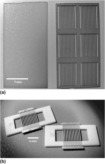
P- and N-type Bi2Te3 wafers of 1-inch (25.4 mm) × 0.57 inch (14.5 mm) × 300 μm were cut using a wire EDM. The wafers were then cut into six arrays of 12 legs attached on both ends using a sinker (plunge) EDM [Fig. 1(a)]. The sinker was a tungsten electrode cut to the appropriate dimensions by wire EDM. The arrays were separated from the wafer using a rectangular electrode in a manner similar to a cookie cutter. These “grills” had 7-mm long legs with 0.5 mm of material holding the legs together [Fig. 1(b)]. The leg width was 150 μm and the pitch (leg center-to-center spacing) was 450 μm. Leg dimensions as narrow as 125 μm were demonstrated. Not all of the length of the grill sees a thermal gradient, with the top and bottom 1.5 mm each being in an isothermal environment, which leads to a mismatch between the thermal and electrical paths in the module (since the isothermal TE material is still electrically resistive). To correct for this, grills were placed in a rig that shadow masks the center 4 mm of the legs and gold was sputtered on the ends of these legs [Fig. 1(b)] to provide an electrical shunt. The gold thickness was 12.5 μm on the top face of the legs and slightly thinner on the sides; the bottom face was uncoated.
P- and N-type Bi2Te3 wafers. (a) Wafer as-cut by wire electro-discharge machining (EDM) from Bi2Te3 ingot and after patterning with sinker EDM. (b) Grills with gold shunts placed in alumina carrier plates, ready for stacking.

Alumina carrier plates were produced to hold the legs in a rigid assembly. The alumina carrier plates were cut from 0.020-inch (508 μm) sintered alumina electronic substrates. The slots of 0.0135-inch (343 μm) deep and 0.008-inch (208 μm) wide were cut into the substrates on a 450-μm pitch; these slots accommodate the legs (Fig. 1). Rectangular holes of 4 mm × 7 mm were cut through these grooves with a CO2 laser, and the carrier plates were then freed with a dicing saw. The top and bottom edges of the carrier plates were 1.5-mm wide. The grills were fixed into the carrier plates using a custom-blend, alumina-filled sodium silicate cement. The top and bottom edges of the carrier plates became the continuous surface for contact deposition. The sides provided a robust handle for the module until the final step in which they were trimmed off with a diamond wire saw.
Alumina was selected as the carrier frame for its ready availability and relatively high thermal conductivity for a ceramic (24.7 W/m-K). The coefficient of thermal expansion (CTE) is not optimal compared to bismuth telluride (5 ppm/°C versus 16 ppm/°C), but for such small pillars and relatively low thermal excursions this has not proven problematic. MgO was considered because it has a much higher CTE and even higher thermal conductivity, but it is not as readily available.
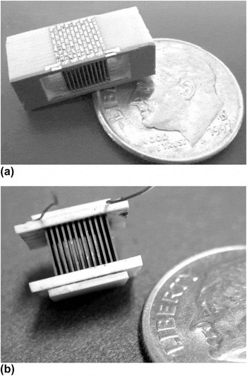
Alternating assemblies of carrier plates and P- and N-type material were stacked and cemented together using the custom-blend silicate cement to build the module. The cement was cured at low temperature, then facing cuts were made with oil lubricant to expose the ends of the legs. The gold shunts on the legs are simultaneously exposed, allowing for gold-to-gold connections during the deposition of the interconnects [Fig. 2(a)]. The interconnects were deposited by evaporation and included a thin (40 nm) Ti adhesion layer and a thick (12.5 μm) layer of Au. Electrical leads were attached with Au/Sn solder (Tmelt = 280 °C). Plates of alumina were cemented to the top and bottom of the generator to protect the interconnect during mounting of the module to external heat sources and sinks. The final module is shown in Fig. 2(b).
Assembled module. (a) After facing cut and interconnect deposition. (b) Fully assembled.

The inorganic adhesive selected is sodium silicate with alumina filler (∼25 wt%). A number of cements were considered (such as Zn phosphate, Al phosphate, and sodium silicates with various fillers), although typically, the mechanical strength of these cements is low when diluted to the point that they flow well in the fine features of this device. Sodium silicate solution (40 wt% in water) has excellent flow properties and makes a strong bond, but the material is intumescent, leading to foaming during the curing process. Alumina fill was added to reduce the foam cell size such that the interconnect pattern can reliably be made across the joints. A stronger, but more viscous, Al phosphate cement is used to bond the protective cover plates over the interconnects.
B. Interconnect evaluation
The selection of gold for the interconnect material was made based on literature review, but a series of tests were performed to confirm its suitability in this application. Gold films were sputter deposited onto Bi2Te3 tiles and annealed (100–250 °C) under vacuum for up to 30 days. Cross-sectional scanning electron microscopy was performed to check for any signs of compound formation or changes in film morphology. Auger spectroscopy was used to determine the effect of cleaning procedures on the surface composition of bismuth telluride. Thin film adhesion tests were performed by attaching a pin to the film with epoxy and pulling perpendicular to the surface with a Sebastian V pull tester. Measurements of contact resistance and bulk resistivity on bulk samples were made using a custom multipoint probe in the manner described by Liao et al.Reference Liao, Lee and Chen14
C. Module evaluation
Module testing was performed at equilibrium [direct current (DC)] and by impedance spectroscopy and the Harman technique [alternating current (AC)] at several temperature gradients. All testing was performed in high vacuum (<5 × 10⁻⁵ Torr) to minimize convective thermal losses. DC measurements were performed using a specially designed rig consisting of a resistance heater embedded in gold-plated heat shields. A combined thermal and electrical model was created to represent the modules in the test stand. A one-dimensional resistor network model with five nodes and 12 resistors (including thermal resistors representing the thermocouples attached to the test stand) was used to represent the test stand. A three-dimensional finite element model of the test stand was also generated to provide more fidelity of select experimental conditions. Peltier cooling, Thompson heating, and Joule heating were included in the thermal model. Thermal contact resistances were measured separately in vacuum using a Kapton electric heater and an alumina block flux sensor. A fixed power input was applied to a resistance heater in contact with the modules. The open circuit voltage and temperature difference were measured during heating to determine the Seebeck coefficient. Thermocouples were positioned on the alumina plates on either side of the TE material. A constant load voltage was applied, and the system was allowed to reach equilibrium to determine the power output of the modules; equilibrium was reached in approximately 16 h. A rapid linear DC staircase voltage sweep was performed after equilibration to determine a power curve for each equilibration condition and obtain the module internal resistance. High V versus I regression coefficients (R 2 > 0.995) and impedance spectroscopy were used to verify Peltier effect were negligible during the DC voltage sweep.
Modules tested by impedance spectroscopy were suspended in a vacuum chamber by 0.008-inch (203 μm) diameter copper or Kulgrid wire (Ceramawire, Elizabeth City, NC). Frequency sweeps were performed from 100 kHz to 1 mHz with a 1 mA AC signal. Module ZT, intrinsic resistivity, and Seebeck coefficient were evaluated using the technique described by Downey et al.Reference Downey, Timm, Poudeu, Kanatzidis, Shock, Hogan, Yang, Hogan, Funahashi and Nolas15, Reference Downey, Hogan and Cook16 Thermal conductivity values were assumed to be unchanged from the bulk material.
Measurements of ZT performed on bulk material were made over the temperature range of 30–250 °C, and the functions derived from these measurements were used as inputs to the model. The average contact resistance between P- and N-type elements (3 × 10⁻⁵ Ω-cm2) with gold interconnect was measured and included in the model, but this assumption was checked by comparing measured internal resistance to bulk resistivity values. Thermal diffusivity was evaluated using a pulse diffusivity measurement technique described elsewhere.Reference Gustafsson17 Thermal conductivity was found from the thermal diffusivity and measurements of the specific heat using a differential scanning calorimeter. Mechanical tests (shear and fatigue) of complete modules and grill assemblies also were performed.
III. RESULTS AND DISCUSSION
The fabrication of a module with 4-mm-long free-standing bismuth telluride alloy legs and a cross-sectional area of 4.5 × 10⁻⁸ m2 (150 μm × 300 μm) is, to our knowledge, a novel accomplishment. Vasilevskiy formed similar dimension legs (150 μm × 150 μm) in modules using wire EDM but only for pillars of 1.27-mm long, resulting in a lower aspect ratio (5.6 × 10⁴ m−1).Reference Vasilevskiy, Kukhar, Turenne and Masut3 The finest features demonstrated in a complete module fabricated from bulk bismuth telluride alloys were shown by Seiko, with 80-μm square pillars, 0.6-mm long.Reference Paradiso and Starner2 These pillars were cut by a dicing saw. The aspect ratio of these devices is similar to the present work (9.4 × 10⁴ m−1 versus 8.9 × 10⁴ m−1), but this is likely near the limit of the technique. The present design can easily be extended to nearly the 7-mm free-standing leg dimensions demonstrated in the grills, an aspect ratio of 1.6 × 10⁵ m−1, but this aspect ratio is nonoptimal for the application.
A. Interconnect evaluation
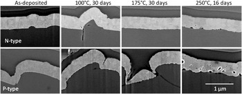
The effect of annealing at near-operational temperatures on Au sputter deposited over eight bismuth telluride alloy samples is shown in Fig. 3. The cut surface from EDM is quite rough at the magnification used here, but the 300-nm gold film is fairly conformal to that surface and appears dense. No compound formation occurs under these conditions; AuTe is possible but was not observed. The gold appears to have high mobility at 250 °C, with some voids forming, particularly on the P-type material. The volume of interfacial voids is comparable to what is expected in the N-type bismuth telluride alloy for saturation of this element, so it is probable that the P-type metallization also is showing possible Kirkendall voids. Note that the actual film thickness in the application was increased to 12.5 μm (not 300 nm as shown in these micrographs) to ensure complete coating and minimize resistance between elements.
Sputtered Au films on bismuth telluride after heat treatment under vacuum.

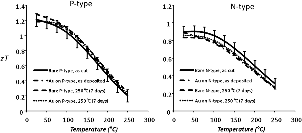
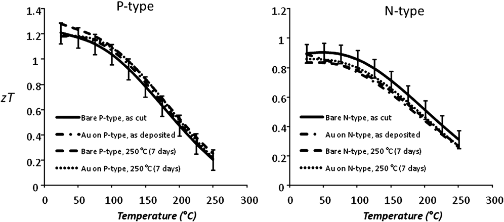
Tests of ZT and contact resistance were performed to confirm that the performance was not degraded after annealing at 250 °C for 7 days, despite the evidence of significant diffusion of Au into the TE materials. Figure 4 shows that there is virtually no change in ZT for either the P- or N-type material; any change in behavior near room temperature is within the ±7% error bands. The contact resistance actually improved significantly after heating (from 4.3 × 10⁻⁵ to 3.6 × 10⁻⁵ Ω-cm2 in P-type and from 5.7 × 10⁻⁵ to 2.3 × 10⁻⁵ Ω-cm2 in N-type). It is believed that diffusion aids in making intimate contact at the interface.
Figure of merit (ZT) measurements on P- and N-type material before and after heating, with and without gold. No significant differences are observed.
The mechanical integrity of the interconnect is as important as the electrical performance. Pull tests were performed on gold films (12.5-μm thick) on P- and N-type material and compared to evaporated Co films and the bulk material properties. Initial tests showed disappointing mechanical strength, approximately 3.7 MPa. This is much lower than the Co films (28 MPa P, 36 MPa N) or the bulk material (89 MPa P, 91 MPa N). A factorial design of experiments (DoE) was performed to determine if cleaning or deposition technique could be varied to improve adhesion. A four-factor, two-level DoE was performed. The factors and levels were deposition technique (evaporation or sputter), abrasive cleaning (performed or not), in situ vapor cleaning (performed or not), and material type (P or N). The abrasive cleaning was immersion in 0.3-μm alumina slurry with surfactant and ultrasonic cleaning for 30 min. The in situ vapor cleaning was either 5 min of a Kaufman ion gun in the evaporation chamber or 5 min of Ar sputter cleaning before deposition.
The direct effect of abrasive cleaning and the interaction between the abrasive cleaning and the vapor etching step were found to be significant (P < 0.05). Abrasive cleaning was found to improve the pull strength by an average of 4.3 MPa. The significant interaction term indicates that vapor etching had a deleterious effect on samples already abrasively cleaned, on average reducing the pull strength by 3.7 MPa compared to cleaned samples. The best overall film adhesion was for films that were abrasively cleaned but not vapor etched, which achieved an average 9.7 MPa. This is over two times higher than the initial work. The adhesion is still quite poor compared to Co films; therefore, protective plates have been included in the final module design.
Surface chemical analysis (Auger spectroscopy) was performed to understand why the vapor etching step may harm the adhesion. Wafers as-cut from wire EDM were placed in the Auger and an elemental quantification was performed. An in situ sputter clean was then performed (250 W for 30 s) and the samples were retested. The carbon and oxygen signals on the samples that were not cleaned were confounding, as expected, so the ratio of Te/cations (Bi + Sb for P-type, Bi for N-type) was used to characterize the results. The Te/cation ratio was high in both as-received wafers (2.67 in P-type and 3.49 in N-type), suggesting that the recast from the EDM process is Te rich. The quick sputter clean produced P-type material that had a Te/cation ratio of 1.58, close to the nominal 1.5. The same sputter etch process resulted in N-type material with a Te/Bi ratio of 0.82. This very Te-depleted material may have reduced mechanical strength compared to stoichiometric Bi2Te3. However, it is likely stronger than the recast layer left by EDM. This explains why sputter etching produces better adhesion than no treatment (4.06 MPa versus 3.7 MPa) but is strongly deleterious to the performance obtained from an abrasive cleaning process (9.7 MPa). Interestingly, it appears that sputter etching (4.1 MPa) is worse for the film adhesion than ion milling (7.1 MPa), but it was not possible to explore this because of limitations on the Auger instrument.
B. Module evaluation: Electrical
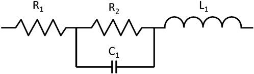
TEM evaluation was performed using nondestructive AC techniques, and then the TEM was permanently integrated into a DC test stand. It was found that reversible techniques for embedding the TEM into the DC test stand (such as pressing the module into indium foil) resulted in poor thermal contact at the interfaces when the module was heated under vacuum. Impedance spectra were fit to the model shown in Fig. 5.
Circuit equivalent for thermoelectric module (TEM) tests (replace with model including series inductor).
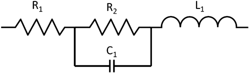
L1 represents the lead inductance, which is negligible below 10 kHz. R1 is the intrinsic resistance of the TE material. R2 is related to the Seebeck coefficient and thermal resistance of the module:
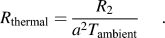
The R2 fit was 82 Ω. This indicates a Seebeck coefficient of 371 μV/K, assuming that the thermal resistance is unchanged from the value predicted from bulk measurements (454 K/W).
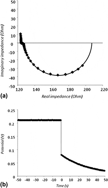
A Nyquist plot of the impedance spectrum is given in Fig. 6. Inductive values (Z″ > 0) are present for very high frequencies (f > 10 kHz), whereas the capacitive component becomes large below 1 Hz. The capacitance is the result of stored thermal energy in the TE legs, and at 0.39 xfarad it is quite large compared to a conventional capacitor. The intrinsic resistance (R) of the TE material is found in the midrange frequency tests. The 1 kHz resistance is 124 Ω.
Transient TEM evaluation (a) Nyquist plot of TEM impedance spectrum. The circle indicates the fit to a capacitive circuit element. (b) Potential versus time plot for Harman technique. Both techniques indicate a module ZT of approximately 0.64.

Module ZT can be found directly from the impedance spectrum using the expression:

RDC is the high intercept of the real axis in the Nyquist plot, and RAC is the low intercept. The module ZT calculated in this manner was 0.64. These resistances multiplied by a DC current produce the voltages measured by the Harman technique.Reference Iwasaki, Koyano and Hori18 The result of a Harman test with a 1 mA DC load (applied for 500 s) is shown in Fig. 6(b). VDC is 0.211 V. VAC is the magnitude of the instantaneous drop in voltage when the current is removed and is 0.130. The resulting ZT is 0.61. ZT of 0.61–0.64 implies a Seebeck coefficient of 357–365 μV/K, assuming a thermal resistance of 454 K/W and the measured electrical resistance of 124 Ω. This is consistent with the circuit model fitting technique result.
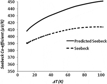
Both AC estimates of ZT assume a completely adiabatic system [x = 1 in Eq. (2)]. The high vacuum environment and long leads are used to make this as close an approximation as possible. Equilibrium testing with a well-characterized test stand (Fig. 7) was used to validate the AC measurements. Open circuit voltage was monitored holding the cold side temperature to approximately 10 °C and creating up to a 100 °C ΔT. The measured Seebeck coefficient was 397 μV/K at an average module temperature of 300 K.
Seebeck coefficient calculated from equilibrium measurements.

The thermal resistance of the module was tested by allowing the module to equilibrate thermally at three different input power levels and measuring ΔT. The thermal model of the TE test stand was used to estimate the fraction of the input power that was transmitted down the TE legs. The average thermal resistance was 475 K/W, slightly higher than the predicted 454 K/W. This may be due to the legs being slightly smaller than the design thickness. The difference in thermal resistance can be accounted for if the actual cross-section was 7 μm smaller in both dimensions of cross-section, well within the 12-μm machining tolerances. The mean error between the thermal model and actual module temperature gradient was 2.7 °C, validating the thermal model. Only approximately 36% of the input heat is transmitted down the TE material legs in the test stand.
The 475 K/W thermal resistance, 124 Ω electrical resistance, and 397 μV/K Seebeck coefficient correspond to a ZT of 0.72. This is close to the predicted ZT of 0.85, indicating that the TE material has not suffered significant damage during the assembly process. The discrepancy between the equilibrium measurements and the AC measurements of ZT are likely the result of nonadiabatic conditions around the module. The ZT discrepancy (0.64 versus 0.72) suggests that the factor x in Eq. (2) is approximately 0.8, meaning 12% of the heat pumped through the TEM is lost to the environment in the AC test setup. Most of this heat is likely lost through conduction along the lead wires to the TEM, with some additional losses through radiation on the module faces.
C. Module evaluation: Mechanical
The fine dimensions of the module legs led to concerns that modules would not be robust enough to survive incidental mechanical loading in any practical application. As an array of tall slender beams, the module was thought to be most susceptible to shear loading. Modules were shear tested in both the stiff direction (perpendicular to the 300-μm beam dimension) and the compliant direction. Failure in the compliant direction occurred at 6.2 N applied load and in the stiff direction at 28.3 N. Shear displacements at failure were 118 and 244 μm, respectively. The axial load response was not evaluated for the reason cited above and because it is practical to build “shock absorbers” that can prevent such a load from being transferred to the device.
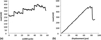
An additional concern was that the material would undergo fatigue failure under cycling at loads significantly below that of the maximum shear load. To evaluate this, a 12-leg array of N-type Bi2Te3 was mechanically cycled with load increases approximately every 10,000 cycles, up to the mean maximum monotonic shear load of similar arrays (430 ± 30 mN). The test included over 10,000 cycles at nearly 100% of this expected failure load [Fig. 8(a)]. The array did not fail so a final monotonic shear displacement test was performed, finally breaking the array near 500 mN [Fig. 8(b)]. This test indicates that even severe cycling of the TE material does not substantially degrade the mechanical performance.
Fatigue testing of 12 N-type leg arrays. (a) Applied load by cycle number. (b) Load–displacement curve as at end of cycle tests.

IV. CONCLUSION
A high-aspect ratio, high-temperature, and high-vacuum compatible bismuth telluride-based TEM with free-standing legs was fabricated. Wire and sinker EDM was used to fabricate legs, which are 150 μm × 300 μm in area and 7-mm long. Gold was used to create high-temperature compatible interconnect. A novel ceramic carrier plate process was used to handle the delicate legs. The fabrication process did not significantly damage the material as module ZT was 0.72, 85% of the expected value based on measurements of bulk properties including contact resistivity. A carefully modeled test stand was used to estimate the thermal transport down the legs to determine the module ZT under a thermal gradient in high vacuum. Impedance spectroscopy and the Harman technique were used to determine module ZT prior to integration in the test stand. These techniques indicated a ZT of 0.64, likely due to thermal losses during testing. Mechanical testing of the module indicated good robustness under cycling and a 6.2 N maximum shear load in the most compliant direction.
ACKNOWLEDGMENT
Sandia National Laboratories is a multiprogram laboratory operated by Sandia Corporation, a wholly owned subsidiary of Lockheed Martin Corporation, for the U.S. Department of Energy’s National Nuclear Security Administration under Contract DE-AC04-94AL85000.