Introduction
Electron sources with plasma cathodes are a type of electron-beam device that operates based on electron emission from the plasma of a glow or arc discharge (Oks, Reference Oks1992; Devyatkov et al., Reference Devyatkov, Vorobyov, Koval and Shugurov2015; Koval et al., Reference Koval, Devyatkov, Nguyen and Uglov2015). The main advantage of the plasma electron sources is its ability to operate at a higher pressure compared with hot-cathode sources (Gleizer et al., Reference Gleizer, Krokhmal, Krasik and Felsteiner2003; Burdovitsin and Oks, Reference Burdovitsin and Oks2008). Plasma electron sources are not demanding with respect to gas atmosphere and vacuum conditions, have a long life, and high emission current density. High temperature of the electrons in the beam, as compared with hot-cathode sources, does not allow using such sources to generate beams of high brightness typical of hot-cathode sources. However, recent studies indicate that this difference is not so great (Kornilov et al., Reference Kornilov, Osipov and Rempe2009; Bakeev et al., Reference Bakeev, Dvilis, Klimov, Oks and Zenin2018a, Reference Bakeev, Klimov, Oks and Zenin2018b). As of today, there have been a large number of plasma electron sources being developed varying in design, parameters, and applications (Gleizer et al., Reference Gleizer, Krokhmal, Krasik and Felsteiner2003; Burdovitsin and Oks, Reference Burdovitsin and Oks2008; Kornilov et al., Reference Kornilov, Osipov and Rempe2009; Devyatkov et al., Reference Devyatkov, Vorobyov, Koval and Shugurov2015; Akishev et al., Reference Akishev, Karalnik, Medvedev, Petryakov, Trushkin and Shafikov2017; Akishev et al., Reference Akishev, Aponin, Karalnik, Petryakov and Trushkin2018; Bakeev et al., Reference Bakeev, Dvilis, Klimov, Oks and Zenin2018a, Reference Bakeev, Klimov, Oks and Zenin2018b). Among the most needed applications of plasma electron sources, one can highlight welding, metal and alloy melting, dimensional processing, evaporation and subsequent surface coating, medical instrument treatment, and even food sterilization (Kim et al., Reference Kim, Fan, Cho, Eo, Park, Kim, Lee and Lee2015; Węglowski et al., Reference Węglowski, Błacha and Phillips2016; Pillai and Shayanfar, Reference Pillai, Shayanfar, Venturi and D’Angelantonio2017).
The so-called forevacuum-pressure plasma sources, which enable processing of non-conductive dielectric materials (ceramics, polymers, glasses, etc.), occupy a special place in the total assortment of plasma electron sources (Goreev et al., Reference Goreev, Burdovitsin, Klimov and Oks2012; Burdovitsin et al., Reference Burdovitsin, Dvilis, Zenin, Klimov, Oks, Sokolov, Kachaev and Khasanov2013; Bakeev et al., Reference Bakeev, Dvilis, Klimov, Oks and Zenin2018a, Reference Bakeev, Klimov, Oks and Zenin2018b). These sources operate in a pressure range from a few to a few tens of pascals, which is one or two orders of magnitude higher than the working pressure of conventional plasma sources (Zenin et al., Reference Zenin, Klimov, Burdovitsin and Oks2013). At such pressure, the electron beam transport is accompanied by the formation of plasma with a concentration of order 1016/m3, which is sufficient to practically compensate the negative charge carried by the beam electrons onto the irradiated target (Burdovitsin et al., Reference Burdovitsin, Klimov and Oks2009). The electric potential of the target surface within the processed area does not exceed several hundreds of volts and does not noticeably change the electron beam energy, much less deflect it off the processed area as is the case at higher vacuum. Thus, in the forevacuum range of pressure, the energy transfer to the irradiated target is close to 100%, which is an undoubted advantage of such type of sources.
Here we present the design, main parameters, and characteristics of the latest modifications of the forevacuum plasma electron source based on a hollow-cathode discharge which provides higher values of the electron beam-specific parameters.
Forevacuum plasma electron source
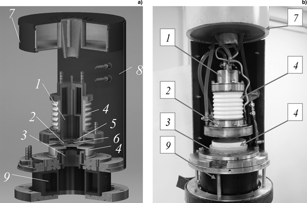
An illustration and a photograph of the forevacuum plasma electron source are shown in Figure 1.
Illustration (a) and (b) photograph of the forevacuum plasma electron source. 1 – hollow cathode; 2 – plane anode; 3 – extractor; 4 – metal-ceramic insulator; 5 – cathode replacement insert; 6 – tantalum emission electrode; 7 – caprolon cylinder with water high-voltage isolator; 8 – steel body frame; 9 – body of the magnetic lens.

The design of the electron source consists of two main units: a discharge cell to generate the emission plasma, and the electron extraction and acceleration system. The plasma electron sources normally use a glow or an arc discharge to generate plasma (Oks, Reference Oks2006). The most suitable discharge system for generation of the emission plasma in the forevacuum pressure range is a hollow-cathode glow discharge, wherein electron selection is carried out through an anode emission aperture (Oks, Reference Oks2006). This kind of discharge is preferable because of its broad range of working pressure, fully corresponding to the forevacuum pressure range, the possibility to create a high-density plasma in a small volume, relatively low discharge burning voltage, temporal stability of parameters, as well as the possibility to shape the extracted electron beam by changing the geometry of the plasma emission boundary (White, Reference White1959; Sturges and Oskam, Reference Sturges and Oskam1964; Burdovitsin and Oks, Reference Burdovitsin and Oks1999).
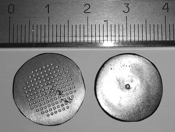
The forevacuum plasma electron source is basically a three-electrode system: hollow cathode 1, plane anode 2, and extractor 3. The source electrodes are electrically insulated using standard metal-ceramic insulators 4. These insulators also serve as a bearing structure for the source. The hollow cathode and the plane anode make up the electron source discharge system. The hollow cathode is a cylinder with an outer radius of 55 mm; the inner part of the cathode cavity is 110 mm deep and consists of two sections of different diameters d 1 and d 2, and lengths l 1 and l 2; see Figure 1. The length of the section's narrow part, located in the region of the cavity opposite to the anode, can vary from 10 to 90 mm. The diameter of the narrow part varies from 8 to 40 mm. The diameter of the wider part is 40 mm. The cathode walls are enclosed in a cooling water jacket. In the wider part of the hollow cathode, there is a threaded hole for screwing replacement insert 5. The insert has an 8 mm-diameter hole and due to varying anode–cathode separation makes it possible to change the emission conditions and the area of the open plasma boundary from which the electrons can reach the anode, thus allowing control of the magnitude of the extracted current to some extent. The anode is shaped as a disk with a 15 mm-diameter hole in the center and has a cooling water jacket. The anode aperture is closed by a 1 mm-thick tantalum plate (emission electrode) 6. This plate has either one emission aperture of 1.5 mm diameter or multiple 0.7 mm apertures (Fig. 2). The anode area from which the emission occurs (a circle of about 10 mm diameter) allows no more than 120 holes of 0.7 mm diameter. The diameter values of 1.5 mm and 0.7 mm for the emission aperture were chosen in order to provide a stable and effective operation of the plasma electron source. At a diameter >1.5 mm, the plasma boundary shifts to the accelerating gap, provoking a diminished dielectric strength of the gap. At a diameter <0.7 mm, the efficiency of electron emission from the plasma decreases significantly. Electron emission from a single aperture provides high electron beam power density, while emission from the multiple-aperture electrode yields high electron beam total current and power. Plate 6 fixes the plasma boundary and plays the same stabilizing role as the emission grid (Oks, Reference Oks2006). Extractor 3 is made of stainless steel and shaped as a truncated cone, with a 15 mm-diameter aperture to allow for the beam passage, threaded on the outer cylindrical surface to make it possible to move it along the system axis. The extractor, as usual, is grounded and the negative pole of the high-voltage source is connected to the anode.
Photograph of multi-aperture and single-aperture emission electrodes.

The anode and cathode are cooled by running water. The water pumping rate through the cooling system maintains the electrode at a temperature not exceeding 30°С. Since the cooled electrodes (anode and cathode) are at a high electric potential with respect to ground, the electron source design provides for installation of a high-voltage insulating water cooling section. The water high-voltage isolator is designed as a plastic tube with an inner diameter 6 mm and a length 4 m. The tube is spiraled onto caprolon cylinder 7. The spiral coils are padded with additional insulating layers. The electron source and the water-cooling system are encased in a 2 mm-thick steel body 8, which effectively protects from X-ray bremsstrahlung radiation. The source electrodes are accessed through a detachable body segment.
The plasma electron source is fed by direct voltage power supply units E1 and E2 connected, respectively, to the discharge and the accelerating gaps. The discharge current I d varies from 0.1 to 1.5 A at a discharge burning voltage of 300–700 V. In the gap between anode 2 and extractor 3, upon applying a corresponding voltage, electron acceleration and initial beam formation take place. The accelerating voltage U a during emission from the single aperture varies from 0.5 to 30 kV and is limited by the onset of intensive X-ray bremsstrahlung radiation. During emission from the multiple-aperture electrode, the accelerating voltage U a, due to the electrode thermal deformation, is limited to a value of 20 kV. The electron beam formed by the source is focused by magnetic lens 9 which also serves as a structural unit of the electron source. The beam current I b varies within the range of 10–350 mA independently of the accelerating voltage. The beam current I b is measured with the help of a Faraday cup.
The source operates under an isobaric gas regime because at forevacuum pressure conditions one would fail to create a pressure drop between the plasma generation and the beam formation regions. The vacuum chamber is pumped down to a pressure of 3 Pa, followed by puffing of the working gas to the required pressure. When changing the working gas, the chamber was first flushed by the new gas for 10–15 min. The pressure was measured by a PfeifferCMR 362 active capacitance gauge whose working principle is independent of the type of gas. A model and a photograph of the electron source are shown in Figure 1. The detachable section of the body is not shown.
Measurements of the electron beam were done using the slit-probe method (Kaur et al., Reference Kaur, Ribton and Balachandaran2015). The essence of the method is based on a continuous and rapid crossing by the beam of two parallel slits behind which is placed a current collector. The collector signal was read by a Tektronix 2024B oscilloscope. The slit width was 100 µm and was selected so as to minimize the measurement error of beam diameter. Because of the small width of the slits, the plasma that is inevitably generated in the forevacuum pressure range along the electron beam propagation path (the “beam-plasma”) cannot penetrate the plate with the measuring slits and reach the collector. As a result, the read current signal completely reflects the distribution of beam current density. The slits were separated by 5 mm. A magnetic coil was used to deflect the electron beam. By changing the coil current, it was possible to deflect the beam at a speed up to 100 cm/s.
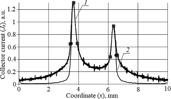
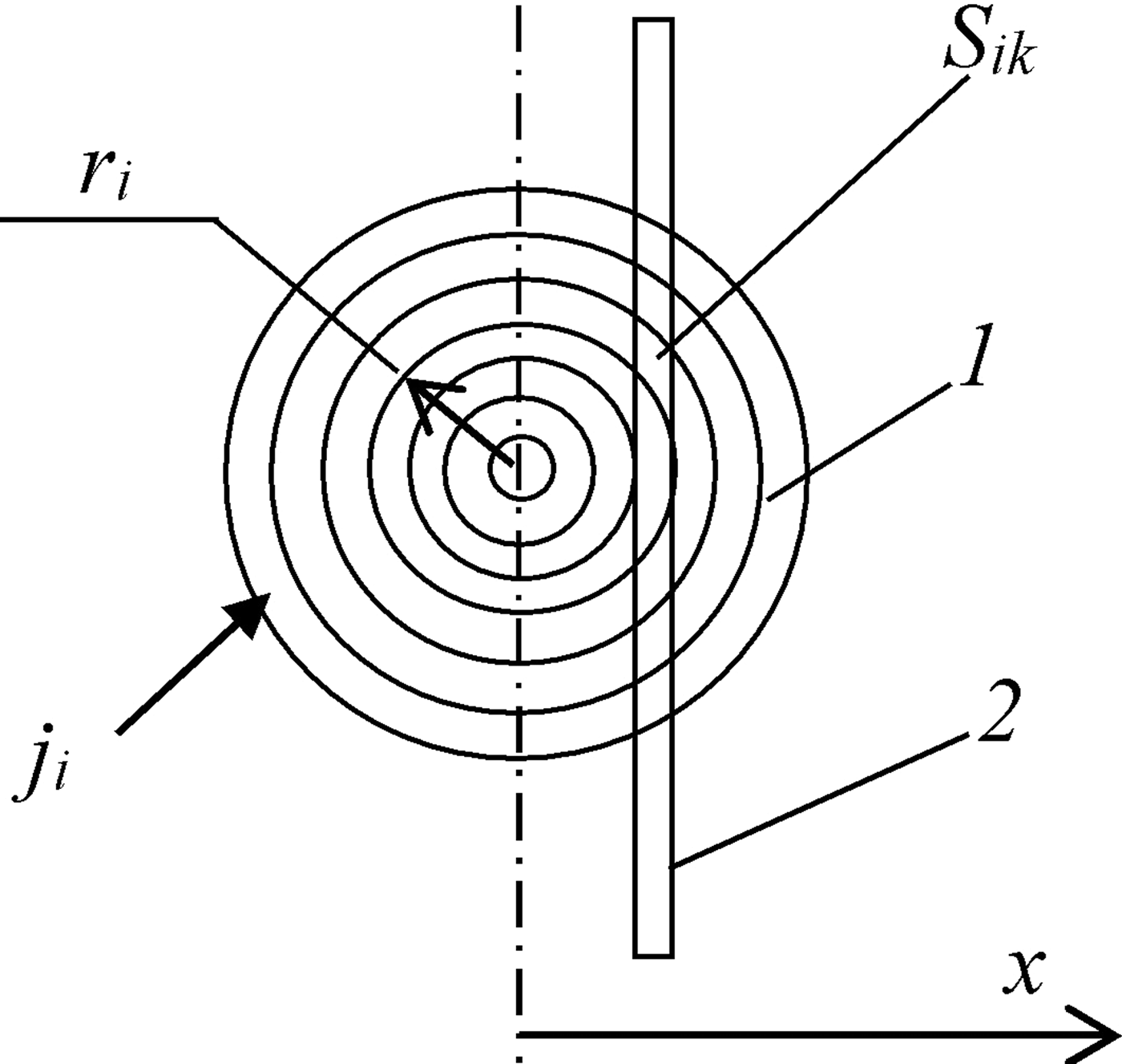
A typical collector current signal read by the oscilloscope is shown in Figure 3 (line 1). Because the beam diameter was calculated based on the radial distribution of beam current density, conversion of the obtained probe distribution j(x) to a radial distribution of beam current density was performed as follows. The distance between the two peaks sets a scale to plot the dependence of probe current density on the coordinate, zero-based at beam center. The coordinate x is calculated as x = L·t/T, where L is the separation between the slits, t is time, and T is the oscilloscope time between the maximums. The current density profile is recovered according to the diagram shown in Figure 4.
The oscilloscope probe signal (1) and the calculated beam current density distribution based on it (2).

Calculation of the radial distribution of beam current density: 1 – beam cross section, 2 – measuring slit.

The electron beam was modeled as a set of tubes with equal current densities j(r). The beam crosscut is made up of a set of concentric rings 1 enumerated beginning from the outmost ring. In this case, the current density profile is
 $$j_e\lpar {x_i} \rpar = \displaystyle{{J_e\lpar {x_i} \rpar -2d\sum\limits_{k = 2}^i {\,j_e\lpar {x_{n-1}} \rpar \left( {\sqrt {x_{n-1}^2 -x_i^2} -\sqrt {x_n^2 -x_i^2}} \right)}} \over {2d\sqrt {x_i^2 -x_{i + 1}^2}}}, $$
where J e(x i) is the current measured at the collector at the point x i, and j e(x i) is the recovered radial profile of the current density at the cross-section at x i.
A typical radial distribution of beam current density j(r) calculated based on the probe signal is shown in Figure 3 (line 2). The beam diameter d b is assumed equal to the width at the half height of the recovered current density distribution.
Parameters and characteristics of the electron source
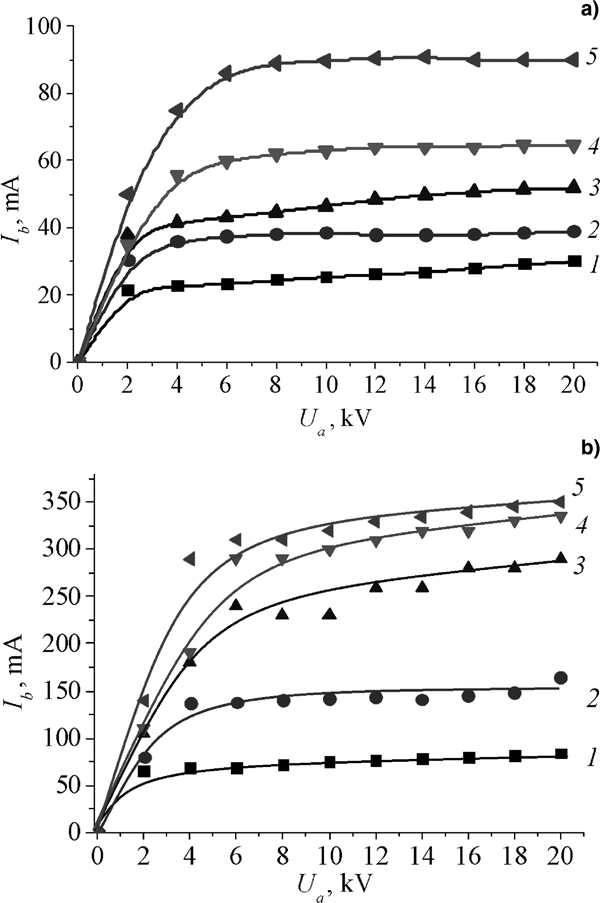
The source voltage–current characteristic for the single-aperture and the multiple-aperture emission electrodes is shown in Figure 5. As seen in Figure 5, the source voltage–current characteristic contains two regions with a close to linear dependence which have different slopes relative to the horizontal axis. Within the range of accelerating voltage 2–4 kV (depending on the discharge current), a sharp increase in the collector current is observed which then slows down and a saturation trend appears, demonstrating behavior characteristic of plasma electron sources and confirming the presence of an accelerated electron beam.
Dependence of beam current on the accelerating voltage for different emission electrodes: (a) single-aperture, (b) multiple-aperture emission electrode. Discharge current: (1) 300 mA, (2) 600 mA, (3) 900 mA, (4) 1200 mA, (5) 1500 mA.

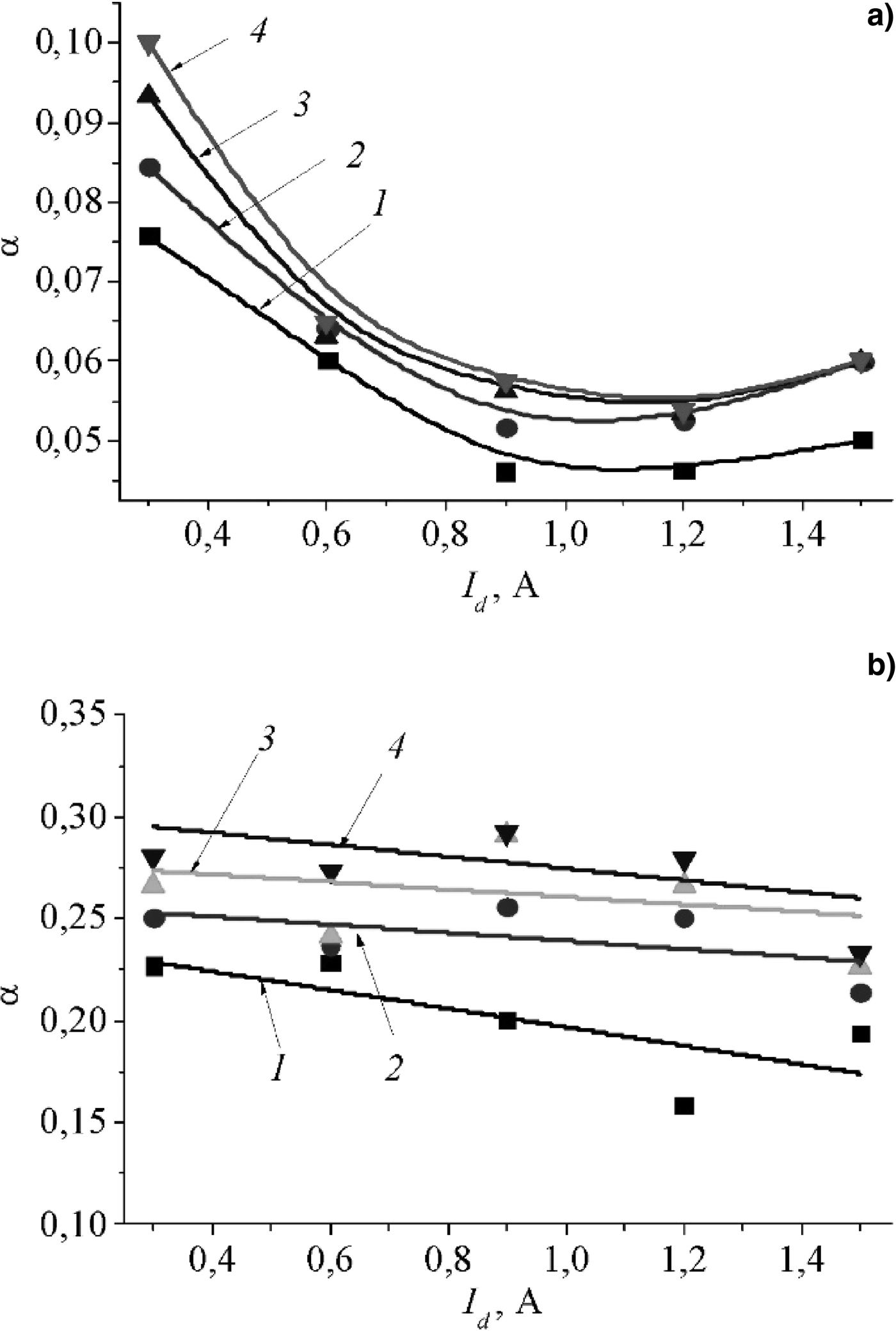
The electron extraction efficiency α = I b/I d (ratio of the beam current to the discharge current) is an important parameter describing the electron source. The dependences of electron extraction efficiency on the discharge current for the two types of emission electrodes are shown in Figure 6.
Dependences of the electron extraction efficiency on discharge current for the two types of emission electrodes: (а) single-aperture, (b) multiple-aperture emission electrodes. Accelerating voltage: (1) 5 kV, (2) 10 kV, (3) 15 kV, (4) 20 kV.

As should be expected, the most efficient electron extraction is observed for emission using multiple apertures. The efficiency of electron extraction through the multiple-aperture electrode reaches 0.32, while the maximum efficiency for the single-aperture emission does not exceed 0.1. Besides, an increase of the discharge current lowers the extraction efficiency from the single aperture by a factor of two, which is apparently due to current interception by the anode. In the case of the emission from multiple apertures, the drop-off of efficiency is observed only at small values of the accelerating voltage, <5 kV. With an increase of the accelerating voltage, the efficiency increases and remains practically constant for the whole range of discharge current.
Since electron sources are designated for electron-beam processing of dielectric materials, including those with an intense gas release during irradiation (e.g., ceramic or metal powders), the gas pressure in the working chamber during electron-beam treatment can increase by a factor of several. In this regard, we have studied the dependence of the electron beam diameter on the vacuum chamber pressure.
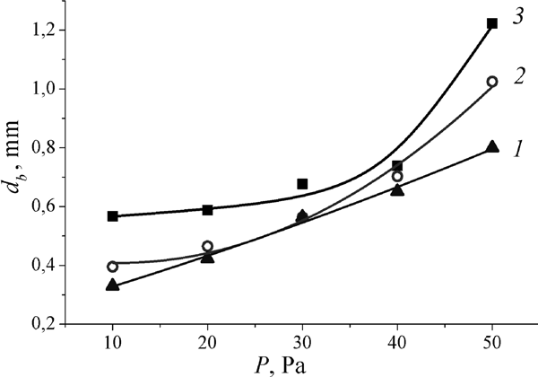
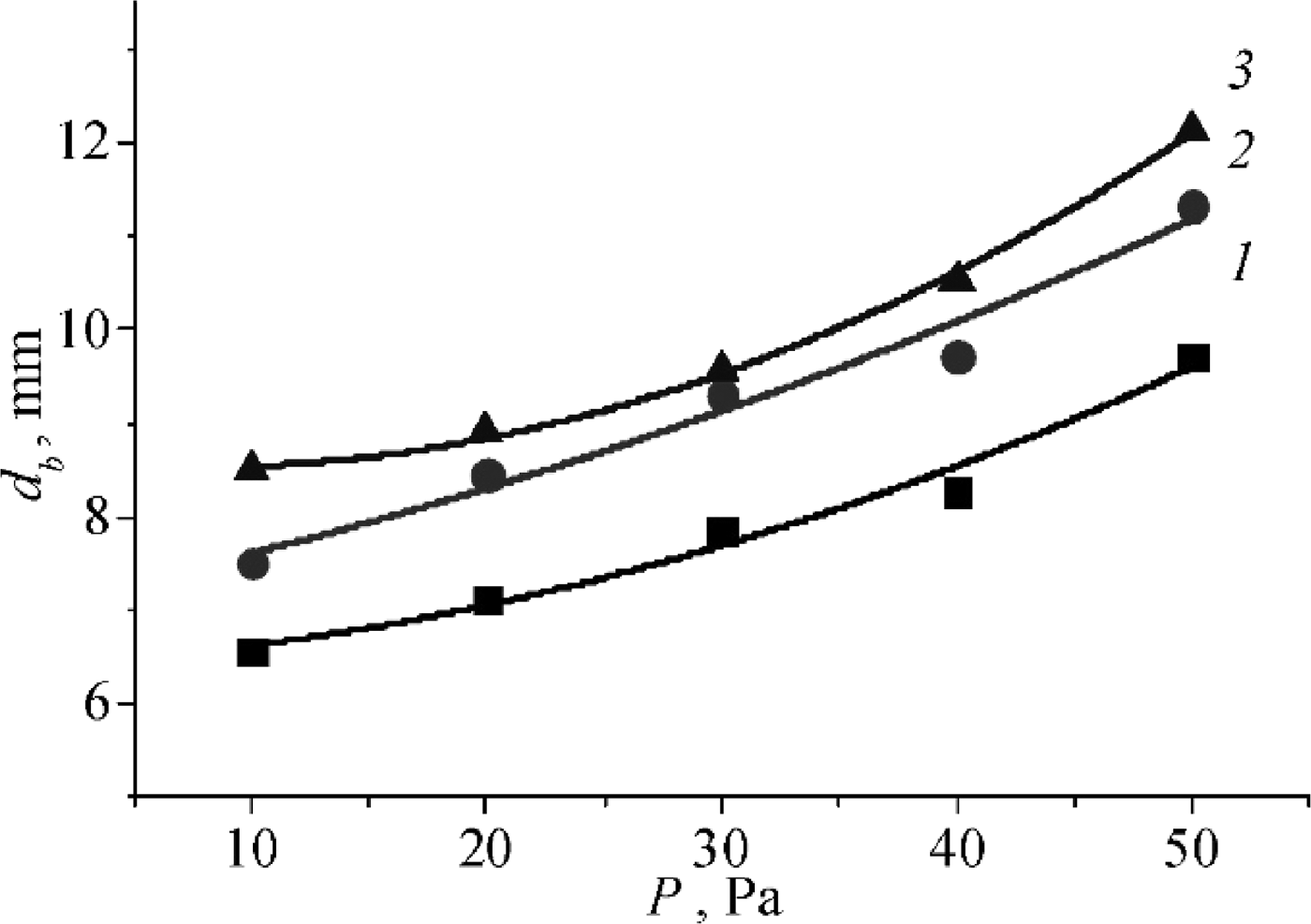
The dependence of beam diameter on pressure for the single-aperture emission is shown in Figure 7 and for the multiple-aperture electrode in Figure 8.
Dependence of the beam diameter on pressure for the single-aperture emission at different beam current: (1) 15 mA, (2) 30 mA, (3) 90 mA. The accelerating voltage is 30 kV.

Dependence of the beam diameter on pressure for the emission from multiple apertures at different beam current: (1) 50 mA, (2) 100 mA, (3) 150 mA. The accelerating voltage is 20 kV.

The dependences of the electron beam diameter for different numbers of apertures determine the possible applications of the forevacuum plasma electron source we have described. For the single aperture, one can create a narrow beam with diameter <0.8 mm over a broad range of helium pressure, 10–40 Pa, and an electron beam power density of 106 W/cm2. In the case of the multiple-aperture emission electrode, the beam power density of 104 W/cm2 is two orders of magnitude less. Thus, the electron beam emitted from the single aperture can be used for localized action on dielectrics (ceramics, polymers, glass, etc.). The emission from the multiple-aperture electrode makes it attractive to use such electron beams for material heating and melting.
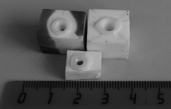
The use of a low-power density beam with a diameter of several millimeters allows heating large areas of alumina ceramics and weld tubes with a diameter up to 20 mm. The emission from the single aperture can be applied for milling and drilling deep holes in ceramic or glass, of diameter <1 mm and up to 70 mm deep (Fig. 9).
Samples of alumina ceramic with a hole made by the electron beam.

Conclusion
In this paper, we have presented the design and main parameters of a plasma electron source capable of generating an electron beam over a wide range of pressure, 10–50 Pa. We have explored the primary characteristics of the electron beam (beam current, beam diameter, power density) depending on the electron source parameters for two types of emission electrodes.
It is shown that, depending on the number of apertures made in the emission electrode, there are realized different beam generation regimes: in the case of a single aperture, the generated beam has a power density of 106 W/cm2 and a diameter of 0.8 mm and is suitable for performing localized action on materials; in the case of 120 apertures, the beam diameter is 6–12 mm and the power is 3 kW making such beams attractive in applications requiring heating, melting, and evaporation of materials.
Author ORCIDs
Ilya Bakeev, 0000-0001-6807-3757.
Acknowledgements
This work was supported in part by the Russian Foundation for Basic Research, grant No 18-38-20007. E.O. is the executor of work on the topic “Organization of scientific research” No. 3.6441.2017/6.7. Special thanks to Dr. Ian Brown (Berkeley Lab) for English correction and useful discussion.