Introduction
Diamond and graphene are common carbon allotropes and have numerous potential applications in electronic devices. Diamond, the sp 3 carbon allotrope, can be employed in high-power devices due to its excellent physical properties, including exceptional thermal conductivity (22 W/cm K), a high electric breakdown field (>10 mV/cm), and a high carrier mobility (∼4500 cm2/V s) [Reference Kasu, Ueda, Yamauchi, Tallaire and Makimoto1, Reference Kawarada, Tsuboi, Naruo, Yamada, Xu, Daicho, Saito and Hiraiwa2]. In contrast, graphene (the sp 2 carbon allotrope) can be used in high-frequency devices as a result of its very high carrier mobility (∼200,000 cm2/V s) [Reference Geim and Novoselov3, Reference Morozov, Novoselov, Katsnelson, Schedin, Elias, Jaszczak and Geim4] and significant current carrying capacity [Reference Yu, Liu, Sumant, Goyal and Baladin5]. These properties originate from the unique band characteristics of this material, which in turn are associated with Dirac cones. Although both diamond and graphene are important electronic materials individually, more recently the interface between diamond and graphene (i.e., the sp 3/sp 2 interface) has attracted much attention because of the various electronic phenomena associated with it. It has been suggested that heterojunctions using graphene (including vertically aligned graphene) and diamond should exhibit a number of interesting electronic characteristics. As an example, Konabe et al. and Shiga et al. predicted highly efficient photoelectric conversion by multiple exciton generation and spin polarization without magnetic ions at the interfaces between diamond and vertically aligned graphene nanoribbons [Reference Konabe, Cuong, Otani and Okada6, Reference Shiga, Konabe, Shiomi, Yamamoto, Maruyama and Okada7]. Ma et al. demonstrated possible band gap opening and the induction of magnetism in graphene layers within graphene/diamond (111) heterostructures [Reference Ma, Dai, Guo and Huang8]. Therefore, graphene and diamond are important not only on their own, but also as building blocks for novel electronic devices through the use of carbon sp 2/sp 3 interfaces. However, in spite of these interesting theoretical considerations, experimental results regarding the electronic properties of such interfaces have rarely been reported [Reference Yu, Liu, Sumant, Goyal and Baladin5, Reference Wang, Jaiswal, Lin, Saha, Ozyilmaz and Loh9, Reference Ueda, Aichi and Asano10]. To the best of our knowledge, there are no empirical data concerning the electronic properties of diamond/vertically aligned graphene [i.e., carbon nanowall (CNW)] heterojunctions, although there have been a few reports regarding the growth of CNW layers on diamond [Reference Tzeng, Chen, Wu, Lo and Li11]. Crystal growth of CNWs does not require metal catalysts [Reference Davami, Shaygan, Kheirabi, Zhao, Kovalenko, Rummeli, Opitz, Cuniberti, Lee and Meyyappan12, Reference Hiramatsu, Shiji, Amano and Hori13], whereas chemical vapor deposition (CVD) of graphene layers typically does [Reference Ago, Ogawa, Tsuji, Mizuno and Hibino14]. The use of catalysts is generally undesirable when the goal is to obtain layered graphene-based structures such as CNWs.
In the present study, CNW layers were grown on diamond semiconductors. The interfacial and electronic properties of the resulting CNW/diamond heterojunctions were examined in detail. The aim was to demonstrate, for the first time, the feasibility of fabricating novel electronic devices using CNW/diamond (i.e., sp 2/sp 3) interfaces.
Results and discussion
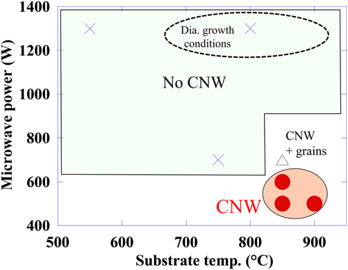
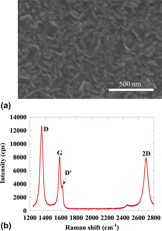
Figure 1 presents a schematic diagram summarizing the growth conditions used to obtain CNW layers on diamond semiconductors. The typical diamond film growth conditions (700–900 °C, 1300 W) are also shown for comparison. The substrate temperature (T S) and microwave power were varied from 500 to 900 °C and 500–1300 W to obtain CNW layers, while maintaining a CH4/H2 flow ratio of 25% (20/80 sccm) and working pressure of 30 torr. During these trials, we attempted to lower the CH4/H2 ratio, but found that a reduced ratio of ∼12.5% resulted in the formation of very small grains (believed to be nanodiamonds) without the fabrication of CNWs. In addition, employing higher microwave power (600–1300 W) and lower T S values (600–800 °C) also did not form CNW layers on the diamond, but rather produced only very small diamond grains (based on SEM observations). Raman analyses indicated that neither CNWs nor graphene layers were formed on diamond under these growth conditions. However, when employing a lower microwave power (less than 600 W) and a higher T S (above 800 °C), CNW structures appeared along with small grains. These grain structures essentially disappeared with increasing T S and decreasing microwave power. In the case of growth at a T S of 900 °C and a microwave power of 500 W, numerous linear wall-like structures with lengths and widths of ∼1 μm and ∼10 nm were observed by scanning electron microscopy (SEM) [Fig. 2(a)]. The Raman spectra of these layers on the diamond [Fig. 2(b)] clearly show three peaks. These include a G peak at 1580 cm−1 and a 2D peak at 2700 cm−1, which are typical of graphene layers, in addition to a D peak, which is related to defect and/or edge formation in sp 2 structures, at 1350 cm−1. The ratio of the D peak intensity to that of the G peak, which correlates with the in-plane sp 2 crystallite size, was found to be ∼1.5, indicating small grain sizes in the graphene-based layers. The G peak was accompanied by a shoulder peak (D′) at 1620 cm−1, which is indicative of disorder-induced phonon modes and also characteristic of CNWs [Reference Kondo, Kawai, Takeuchi, Yamakawa, Den, Kano, Hiramatsu and Hori15]. These combined SEM and Raman results suggest that CNW layers were successfully grown on the diamond semiconductors when applying these growth conditions. The average CNW growth rate was estimated to be on the order of 0.5 nm/min based on atomic force microscopy (AFM) assessments. It is evident that CNWs were generated more readily at a higher T S and a lower MW power, both of which are thermodynamically more stable conditions than those for producing diamond. This is not unexpected, because graphite (including graphene and CNWs) is the most thermodynamically stable phase of carbon at atmospheric pressure, while diamond (which is the high-pressure phase) is thermodynamically unstable. Therefore, to obtain CNWs in situ, it is important to use a higher CH4/H2 ratio (∼25%) with a lower microwave power (∼500 W) compared to those employed for diamond (∼1%, 1300 W). A high H2 flow rate should also be avoided during CNW growth because plasma-excited H2 species behave as effective etchants of amorphous and/or graphitic carbon forms such as CNWs [Reference Kobashi, Nishimura, Kawate and Horiuchi16]. The data obtained in this study suggest that a higher T S, a lower MW power, and a higher CH4/H2 ratio are vital to forming CNW layers on diamond via an in situ process.
Growth conditions used to obtain CNW layers on diamond semiconductors.

(a) SEM image and (b) Raman spectrum of CNW layers on diamond semiconductor, formed at a T S value of 900 °C and a microwave power of 500 W.

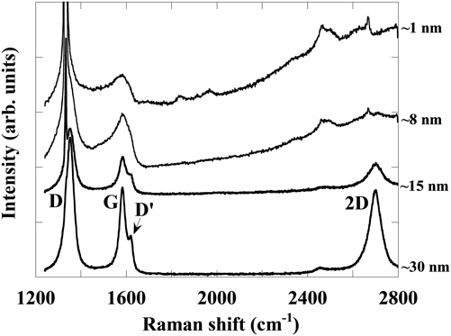
Figure 3 plots the Raman spectra of CNW layers having various thicknesses on diamond semiconductors. The thickness of each CNW layer was controlled by varying the deposition time. Note that these spectra have been offset vertically for better visibility. Both G and 2D peaks, which are typical of graphene and graphite layers, are observed, although the intensities of both peaks decrease as the thickness decreases. D′ peaks, which are characteristic of CNWs, are also present, and again the peak intensity decreases along with the thickness. The D′ peak transitions to a broad shoulder on the G peak in the case of thinner films. Although D peaks, which are related to graphene edges, are clearly observed in the spectra of thicker films, the D peaks for thinner films (<15 nm) are obscured by a sharp peak at 1332 cm−1 due to the first-order zone-center vibrational mode of diamond [Reference Nemanich, Glass, Lucovsky and Shroder17]. The CNW spectra obtained from thinner films exhibit characteristic features, including D′ and D peaks along with G peaks. This result suggests the formation of CNW layers from the initial growth stage, in agreement with the transmission electron microscopy (TEM) results presented below. The Raman results also demonstrate that CNW layers close to the interface were less crystalline, because the G and 2D peaks became much broader in the case of the thinner films.
Effect of thickness on Raman spectra of CNW layers on diamond semiconductors.

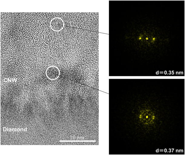
Figure 4 provides a cross-sectional TEM image of a CNW/diamond interface fabricated at a T S of 900 °C and a microwave power of 500 W. The fast Fourier transform (FFT) results for two typical regions at the interface are also shown. The TEM image demonstrates the growth of vertically aligned graphene multilayers (i.e., CNWs) on the diamond. The interlayer spacing of each graphene layer was estimated to be from 0.35 to 0.37 nm based on the FFT analysis. This value is slightly larger than that for standard graphite with AB stacking (∼0.334 nm) [Reference Kolmogorov and Crespi18]. The reason for the larger interlayer spacing in the CNW layer is not clear at present, although it can possibly be attributed to slight oxidation of each graphene sheet and/or different stacking of the graphene sheet (AA stacking, etc. [Reference Kolmogorov and Crespi18]) in the CNW. In the case of CNW layers closer to the interface, the interlayer spacing was slightly larger while the degree of crystallinity was lower than those close to the surface. We attribute these results to hydrogen termination at the diamond surface during the CVD growth process in the plasma-excited H2, which disturbed the direct formation of CNW layers. Thus, less crystalline CNW layers were initially grown on the diamond and subsequently acted as self-buffer layers to form more highly crystalline CNWs. Consequently, the CNW layers close to the surface show a higher degree of crystallinity. Together, these SEM, Raman, and TEM results suggest that CNW layers were grown on the surfaces of diamond semiconductors although crystal quality of the CNW at the interfaces has much room to improve, and that the CNW/diamond heterostructures fabricated in this manner had interfaces of sufficient quality to allow the formation of junctions.
TEM image of CNW/diamond interface, along with FFTs of two typical interface regions.

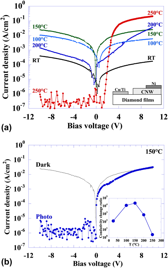
Junctions were fabricated using heterostructures composed of ∼30 nm thick CNW layers on diamond [Fig. 5(a) inset] and the I–V characteristics of these devices were examined in detail. Figure 5(a) summarizes the I–V characteristics of a junction at temperatures from room temperature (RT) to 250 °C. These data demonstrate ohmic behaviors (i.e., a lack of rectification) up to 200 °C. The associated activation energy (E a) was estimated from Arrhenius plots of the forward current density at +10 V. A value of 0.4 eV was obtained, which is in good agreement with the reported E a for B acceptors in diamond of ∼0.37 eV [Reference Borst and Weiss19]. Therefore, the increase in current density from RT to 200 °C is ascribed to the increasing activation of B acceptors in the diamond at higher temperatures. In contrast, the current density in the negative bias region decreased above 200 °C and became minimal at 250 °C. The I–V curves exhibit rectification-like behavior at 250 °C, and the current difference between the negative and positive bias regions exceeds a factor of 106. We believe that this behavior was different from the typical characteristics of Schottky diodes based on p-type diamond semiconductors, which have larger current in the negative bias region. This is the opposite trend to that exhibited by Schottky diodes.
(a) Temperature dependence of I–V characteristics of CNW/diamond junctions, from RT to 250 °C. The inset shows a schematic of the CNW/diamond junction. (b) I–V characteristics of junction with and without white light irradiation at 150 °C. The inset plots the current density change at −10 V upon photoirradiation of the junction as a function of temperature.

A large conductivity change was also observed in response to irradiation with white light from a fluorescent lamp, below 200 °C [Fig. 5(b)]. The conductivity change ratio, defined as the resistance under dark conditions divided by that under photoirradiation, was found to increase with increasing temperature. The ratio reached a maximum value of ∼104 at 150 °C and decreased to ∼102 above 150 °C [Fig. 5(b) inset]. This decrease above 150 °C likely occurred as a result of heat-induced conductivity changes. These results suggest that the conductivity of CNW/diamond junctions can be controlled by applying either photoirradiation or heat. The effects of both photoirradiation and heat on the current are ascribed to the unique nature of the CNW/diamond (sp 2/sp 3) interfaces, because this unusual behavior was not observed during control experiments using Ni/graphene, Cu/Ti/diamond (ohmic), and Ni/diamond (Schottky) junctions.
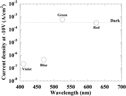
The effects of the irradiation wavelength on the I–V characteristics of these junctions were assessed to assist in determining the mechanism by which photoirradiation or heat induces large conductivity changes. Figure 6 plots the current density for CNW/diamond junctions at −10 V and RT as a function of the wavelength. It is evident that the current density significantly decreases upon irradiation with violet or blue light (∼400–500 nm). In fact, at these wavelengths, a current decrease of about ∼103 was observed for all temperatures below 200 °C. In contrast, the current in response to irradiation with green or red light was almost the same as that obtained under dark conditions. These results confirm that the CNW/diamond junctions have light wavelength selectivity. The energy of blue or violet light is approximately 3 eV, which is much less than the band gap energy for diamond (∼5.5 eV), indicating that carriers generated by band gap excitation did not contribute to the photoinduced change in current. Therefore, the significant variations in conductivity cannot be explained using standard photodiode models in which photoexcited carriers in the semiconductor play a dominant role [Reference Chen, Aykol, Chang, Levi and Cronin20].
Effect of light wavelength on current density for CNW/diamond junction at bias voltage of −10 V. The junction was irradiated using violet, blue, green, and red LEDs. The current density under dark conditions is also shown for comparison.

The effect of the blue light irradiation power on the I–V characteristics was also examined, using blue light, and the degree of current change was estimated by subtracting the current density measured at −10 V under photoirradiation from that under dark conditions. The current density in the negative bias region was found to decrease as the power increased, whereas the current in the positive bias region was almost unchanged. The photoresponsivity of the CNW/diamond junctions was estimated to be 12 A/W below a power level of 0.06 mW/cm2, based on the slope of the plot of current change versus power, although this effect plateaued above 0.1 mW/cm2. This photoresponsivity is approximately two orders of magnitude larger than that reported for commercial photodetectors using other materials, such as Ge (∼0.24 A/W) [Reference Colace, Masini, Galluzzi, Assanto, Capellini, Di Gaspare, Palange and Evangelisti21, Reference Zeng, Wang, Hu, Nie, Yu, Wu, Wang, Hu, Xie, Liang and Luo22]. These results indicate that CNW/diamond junctions could also be used as high-sensitivity photodetectors responding to blue or violet light.
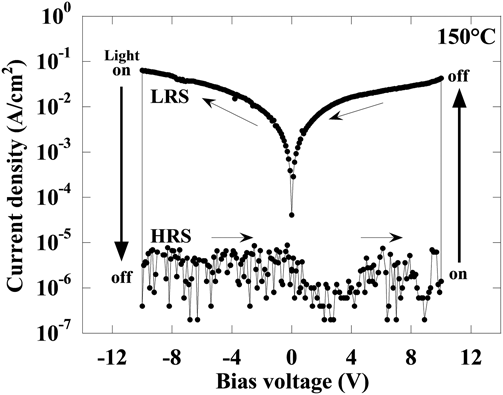
Figure 7 shows the I–V characteristics of the CNW/diamond junctions at 150 °C under blue light irradiation. To obtain the I–V data in Figs. 5 and 6, irradiation was performed continuously during the measurements. However, the data in Fig. 7 were acquired by subjecting the specimen to irradiation for only ∼30 s at ±10 V. In this case, the junction exhibited hysteresis and the resistance changed between a low-resistance state (LRS) and a high-resistance state (HRS) based on the application of a negative or positive bias. This hysteresis was observed between RT and 200 °C, although the conductivity change ratio gradually decreased as the temperature decreased. The transition between the HRS and LRS resulting from irradiation was maintained even after the irradiation was stopped, suggesting that these junctions could function as nonvolatile memory. This resistive switching behavior is a unique feature of so-called memristors, which have multiple resistance states and can act as nonvolatile memory [Reference Pershin and Ventra23]. This phenomenon is exhibited by numerous oxides, including TiO2, Nb–SrTiO3, and (Pr, Ca)MnO3 [Reference Pershin and Ventra23, Reference Fujii, Kawasaki, Sawa, Akoh, Kawazoe and Tokura24]. However, in a typical memristor, the resistance state can be switched only by the application of a bias without photoirradiation. Photoinduced resistance switching is quite rare and has only been observed in a few materials and heterostructures, all of which have demonstrated relatively low photoresponsivity values on the order of 102 [Reference Wang, Panin, Fu, Zhang, IIanchezhiyan, Pelenovich, Fu and Kang25, Reference Maier, Hartmann, Dias, Emmerling, Schneider, Castelano, Kamp, Marques, Lopez-Richard, Worschech and Hofling26]. Our result is the first report on photomemristive behaviors of CNW/diamond junctions, and extremely large conductivity change (∼106) was obtained. The current change ratio of approximately 106 and the photoresponsivity of approximately 12 A/W exhibited by our junctions are much larger than the previously reported values, and thus these junctions have significant potential for optical applications. It is therefore probable that CNW/diamond junctions have the capacity to act as photocontrollable memristors (photomemristors) with photoswitchable resistance states and multiple nonvolatile memory functionalities.
I–V characteristics of junction measured at 150 °C upon brief irradiation. Blue light irradiation was performed at ±10 V for 30 s. The junction changed between LRS and HRS by photoirradiation in conjunction with an applied bias voltage.

The data reported above demonstrate several aspects of these devices. First, they behave as photomemristors. Second, their resistance state can be switched between the HRS and LRS via the application of a negative and positive bias (i.e., bipolar resistive switching [Reference Pershin and Ventra23]) in conjunction with photoirradiation. Third, their resistance states are also changed by heat, and fourth, these devices are selectively affected by blue or violet light. Finally, it was also determined that air exposure for approximately one day was required to obtain a large conductivity change. From points one and two, it appears that the movement of electrically charged particles (such as oxygen ions and electrons) in response to a bias voltage is the primary factor contributing to the switching behavior. From points three and four, it is evident that the energy for the movement of charged particles is provided by blue or violet light and/or heat. From observation five, components of air (such as O2 and H2O) are evidently necessary to induce a large conductivity change. Although it is challenging to determine the working mechanism of these CNW/diamond photomemristors from only these results, we can postulate a mechanism based on reports of other carbon-based memristors. Carbon materials such as graphene oxides (G-O) [Reference Porro, Accornero, Pirri and Ricciardi27] and amorphous carbon (a-C) [Reference Raeber, Zhao, Mordoch, McKenzie, McCulloch and Partridge28] have been found to act as memristors (i.e., standard memristors switchable by an applied bias voltage). As an example, the resistive change for Al/G-O/Al memristors [Reference Porro, Accornero, Pirri and Ricciardi27] is considered to be induced by oxygen ion diffusion in response to an electric field. The amorphous interfacial layers at the top Al/G-O interface become insulating due to a redox reaction between the Al and G-O that generates Al-O + G-O layers as a result of a positive bias. Upon applying a negative bias, the memristors become conductive via the movement of oxygen to the G-O side to form localized conductive filaments at the interfacial layers. In fact, the movement of oxygen is the most important factor determining the resistive change in this case. It is likely that conductivity changes induced by redox reactions occur in our devices because the surfaces of the diamond films are partly oxidized due to the introduction of a small amount of oxygen during CVD growth. The oxidation and reduction of the graphene sheets in the CNWs would take place based on the movements of the associated oxygen ions. In the case of a-C memristors [Reference Raeber, Zhao, Mordoch, McKenzie, McCulloch and Partridge28], the transition between sp 2 and sp 3 structures in response to the application of an electric field play a dominant role. The local rebonding of carbon (sp 3 ↔ sp 2) was ascribed to the application of a sufficiently high electric field, while the transition from LRS to HRS (or HRS to LRS) occurred upon applying a suitably large negative (or positive) bias voltage. This same electric field mechanism could have occurred in our devices, although we tentatively propose that the observed conductivity switching is due to redox reactions at the CNW/diamond interfaces, because air exposure was required to obtain memristive behavior. The temperature dependence of the I–V characteristics [Fig. 5(a)] also support a redox mechanism. That is, the I–V behavior changed significantly at 250 °C, at which point rectification was clearly observed, demonstrating the onset of the movement of charged particles (in this case, oxygen ions) at approximately 250 °C (corresponding to approximately 45 meV). This value of ∼45 meV coincides with the hopping energy of oxygen, which has been estimated to be in the range of 49–123 meV in carbon materials [Reference Chen, Chang, Chang, Chen, Young, Tsai, Zhang, Chu, Ciou, Lou, Chen, Chen, Zheng and Sze29].
The I–V behaviors in Figs. 5 and 7 can also be explained based on redox reactions at the CNW/diamond interfaces and/or CNW layers. In this redox mechanism, the interfaces and layers become insulating due to the oxidation of graphene sheets in the CNWs and at the interfaces, and conducting due to the reduction of the graphene oxide and the interfaces. In this scenario, the CNW/diamond junction can be regarded as a series resistance formed by a combination of variable resistance elements (R CNW) associated with the CNWs and CNW/diamond interfaces and the resistance of the diamond (R Dia). The former resistance values can, in turn, be varied by the application of irradiation and/or heat. In the case that R CNW is minimal, R Dia will be the dominant resistance in the junction and so the overall resistance will change in conjunction with activation of the B in the diamond, as shown in the I–V results from RT to 200 °C in Fig. 5(a). This scenario corresponds to the LRS of the junction. Conversely, when R CNW is large, it becomes the primary resistance and the junction becomes insulating, thus changing to the HRS state. For this reason, the I–V data acquired under continuous irradiation [Fig. 5(b)] show that the junction changed to the LRS in response to a positive bias together with irradiation, and to the HRS due to a negative bias with irradiation. This mechanism explains why rectification-like behavior is observed in Fig. 5(b). The rectification behavior at 250 °C in Fig. 5(a) also appeared for the same reason (i.e., heat-induced oxidation, which increased R CNW and produced the HRS in the negative bias region). In the case of only brief photoirradiation, the junctions showed hysteretic I–V behavior together with the LRS and HRS, as shown in Fig. 7.
We tentatively propose that the photoswitching behavior of these junctions can be explained by this redox mechanism, although a definitive mechanism cannot be determined using only the present results. Clarification of the associated mechanism should result from more detailed analysis of CNW/diamond interfaces in future work.
Conclusions
In summary, this work demonstrated the fabrication of CNW/diamond (carbon sp 2/sp 3) heterojunctions that behaved as photocontrollable memristors. The conductivity change ratio between the HRS and LRS of the junctions became quite large (greater than 106) at ∼150 °C. These junctions were also found to be sensitive to light in the blue to violet (400–500 nm) range. In addition, the junctions exhibited high photoresponsivity values on the order of 12 A/W, which is much larger than those reported for photodiodes using other materials, such as Ge. This change in photoconductivity is attributed to oxidation–reduction of the graphene sheets in the CNWs and/or the CNW/diamond interfaces through the movement of oxygen ions under a bias voltage, in association with photoirradiation. The data obtained in this study indicate that CNW/diamond heterojunctions could find applications as high-sensitivity optical devices intended for use as photocontrollable nonvolatile memory with switching functions.
Experimental methods
Unintentionally B-doped diamond films were grown on commercial type Ib diamond (100) substrates by microwave plasma CVD [Reference Ueda, Kawamoto, Soumiya and Asano30], using a microwave power and frequency of 1.3 kW and 2.45 GHz, respectively. High-purity gaseous CH4 (6N) and H2 (7N) were used as the CVD sources. The CH4/H2 flow ratio was 0.1–1%, the working pressure was 50 torr, and the growth temperature was 700–900 °C. The films produced were typically ∼1 μm thick. To reduce the amount of residual B in the diamond layers, O2 gas was also introduced (O2/H2 flow ratio of 0.25%). Hall measurements showed typical RT acceptor concentrations and mobilities in the resulting materials of ∼1016 cm−3 and ∼1000 cm2/V s, respectively.
CNW layers were grown in situ on the B-doped diamond semiconductors using the same CVD apparatus. During this process, the growth temperature and microwave power were in the ranges of 500–900 °C and 500–1300 W, respectively. The resulting CNW layers were characterized by Raman spectroscopy, SEM, TEM, and AFM. Junctions with diameters of 40–160 µm were fabricated in the CNW/diamond heterostructures using a standard photolithographic process and reactive ion etching [Reference Ueda, Aichi and Asano10]. Ni and Cu/Ti electrodes (annealed at 650 °C for 30 min to promote metallization and the formation of TiC at the interface) were used to establish ohmic contacts on the CNWs and diamond substrates, respectively. The current–voltage (I–V) characteristics of the junctions were assessed from RT to 250 °C in air, with or without photoirradiation (at 400–625 nm) from visible laser emitting diodes (LEDs).
Acknowledgments
This work was supported in part by a JSPS KAKENHI (number 16H04348) and by research grants from the Toyoaki Foundation, Tatematsu Foundation, Murata Science Foundation, and the Research Foundation for Opto-Science and Technology.