Plasmonics: Converting photons into the nanoscale
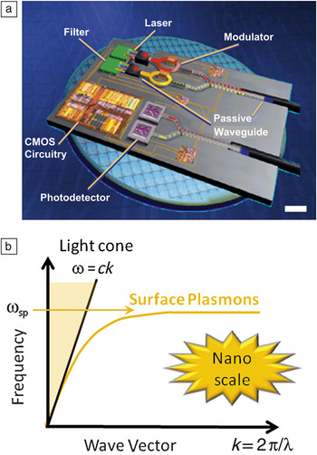
Recently, photonic technologies have become universal in global data communications.Reference Rattner1 The unprecedented data bandwidths, ever falling power consumption requirements, and reduced cost margins of on-chip photonicsReference Paniccia, Krutul and Koehl2, Reference Welch, Kish, Nagarajan, Joyner, Schneider, Dominic, Mitchell, Grubb, Chiang, Perkins and Nilsson3 have established a photonic roadmap for scaling down photonic components.Reference Kirchain and Kimerling4 A solution to fulfil both size and power requirements for future photonic integrated circuit (PIC) technologies lies in photonic components scaled beyond the diffraction limit of light. The advantages of such sub-diffraction limited photonics are three-fold: small physical device sizes, faster operating speeds, and reduced optical power requirements arising through strong light-matter-interaction. To elaborate on the last point, intense optical localization within such components strongly enhances the typically weak interaction between light and matter,Reference Dionne, Diest, Sweatlock and Atwater5–Reference Sorger, Lanzillotti-Kimura, Ma and Zhang7 which in turn reduces the energy necessary to obtain a desired effect, for instance electronic modulation of an optical signal or non-linear optical frequency mixing.Reference Leuthold, Koos and Freude8, Reference Witzens, Baehr-Jones and Hochberg9 In order to address these demands, photonic components and even circuits based on surface plasmon polaritons (SPPs), collective oscillations of electrons at metal-dielectric interfaces, were proposed and are showing promise for the scalability and performance challenges of future PICs (Figure 1a).Reference Barnes, Dereux and Ebbesen10
Plasmonics for emerging ultra-compact and high performance integrated circuits. (a) Schematic of plasmonic integrated circuit components featuring high functionality on small wafer footprints.Reference Paniccia, Krutul and Koehl2 With the strongly enhanced light-matter-interaction of plasmonics devices, the seamless integration of plasmonic and electronic (i.e., complementary metal oxide semiconductor) components featuring similar device lengths is possible. The scale bar being on the order of the operating telecommunication wavelength (1.3–1.55 μm) highlights such nanoscale compact circuit architecture. (b) The unique dispersion relation of surface plasmon polaritons (SPPs), collective electron oscillations at metal-dielectric interfaces, yields extremely high wave vectors (k) capable of producing nanoscale optical fields, where c is the speed of light in vacuum, and ωsp is the surface plasmon polariton angular frequency.Reference Maier11

In this article, we focus on highlighting key features of SPPs that are relevant to PIC technology, such as waveguides, lasers, optical modulators and photodetectors based on enhanced light-matter interactions using plasmonics. In simple terms, plasmonics can be viewed as “light-on-metal-dielectric-interfaces;”Reference Maier11 electrons are collectively accelerated and decelerated at metal surfaces by the electric field of light with its corresponding high frequency. However, because conduction electrons have a high scattering rate from nuclei, phonons, and themselves, they experience significant resistive damping. Depending on the portion of the plasmonic optical field residing in the metal, this loss is manageable in a number of on-chip waveguide architectures such that information can span the short distances between components in future compact plasmonic circuits. The key capability of plasmonics is to go beyond the diffraction limit arising from the involvement of electrons in the propagation of light. In particular, the oscillating electrons bind light to the metal surface to form a surface wave, which exponentially decays into the two adjacent half spaces, giving rise to optical mode sizes of opto-electronic devices below the diffraction limit of light. The (de)accelerated metal electrons increase the momentum of light at the surface, reducing its apparent wavelength and thus allowing field localization beyond the diffraction limit of light, which can be utilized to enhance weak optical effects of opto-electronic devices. Under these conditions, surface plasmons can be viewed as optical transformers; their unique dispersion relation allows for large wave vectors, k, (i.e., small wavelengths) at the surface plasmon frequency (Figure 1b).
Plasmonic waveguides for on-chip communication
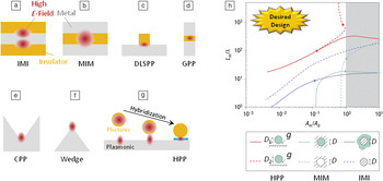
A wide variety of plasmonic waveguide designs have been investigated for the general purpose of on-chip communication.Reference Gramotnev and Bozhevolnyi12 Early studies experimented with nanosized metallic particle chains. While offering remarkably deep subwavelength fields by operating at the surface plasmon frequency, these chains of nanoparticles suffered from strong optical attenuation yielding propagation distances shorter than a single micrometer.Reference Maier, Kik, Atwater, Meltzer and Harel13 However, a number of research groups have investigated surface plasmon propagation along metal waveguides with nanostructuring in two dimensions, motivated by the promise of extremely strong lateral confinement in metal nanowires.Reference Kusunoki, Yotsuya and Takahara14Figure 2 provides an overview of some waveguide architectures considered in the literature, which are all capable of strong optical confinement with manageable propagation losses. However, only a handful of these examples have experimentally achieved confinement beyond the diffraction limit.Reference Sorger, Lanzillotti-Kimura, Ma and Zhang7, Reference Verhagen, Spasenovic, Polman and Kuipers15–Reference Sorger, Ye, Oulton, Bartal, Wang and Zhang17
Surface plasmon waveguide architectures. Shown are the waveguide cross-sections, with the optical data propagating in the third dimension. (a) Insulator-metal-insulator (IMI),Reference Verhagen, Spasenovic, Polman and Kuipers15 (b) metal-insulator-metal (MIM),Reference Dionne, Lezec and Atwater16 (c) dielectric loaded surface plasmon polariton (DLSPP),Reference Steinberger, Hohenau, Ditlbacher, Stepanov, Drezet, Aussenegg, Leitner and Krenn22–Reference Briggs, Grandidier, Burgos, Feigenbaum and Atwater24 (d) gap plasmon polariton (GPP),Reference Jung, Teixeira and Reano19 (e) channel plasmon polariton (CPP),Reference Bozhevolnyi, Volkov, Devaux, Laluet and Ebbesen18 (f) wedge SPP,Reference Pile, Ogawa, Gramotnev, Okamoto, Haraguchi, Fukui and Matsuo20 and (g) hybrid plasmon polariton (HPP).Reference Sorger, Ye, Oulton, Bartal, Wang and Zhang17, Reference Alam, Meier, Aitchison and Mojahedi25, Reference Oulton, Sorger, Pile, Genov and Zhang26 (h) A figure-of-merit comparison for nanoscale waveguides (HPP, IMI, MIM) highlights the achievable propagation distance (L m) in numbers of operation wavelength, λ, to the propagating optical mode size, A m, normalized by the diffraction limit of light, A 0 = λ2/4.Reference Oulton, Sorger, Pile, Genov and Zhang26 A trajectory shows a range of one structural parameter: HPP gap g = [1, 104] nm and core diameters D 1 = 200 nm, D 2 = 215 nm; for IMI and MIM D = [10, 104] nm (red curves). Scaling D of the MIM mode introduces an optical mode cutoff (green curves). The IMI does not suffer from a cutoff, yet the propagation lengths are limited (blue curves). The HPP mode offers both strong optical confinement and reasonably long propagation performance. The gray area highlights mode sizes that are above the diffraction limit. Dashed versus solid curves for IMI and MIM show dielectric (green) versus air cladding (white), respectively. Material relative permittivity: semiconductor = GaAs (εs = 12.25), oxide = SiO2 (εox = 2.25), metal = Ag (εm = –129 + 3.3i), and λ = 1550 nm. Note: E-field, electric field.

It is remarkable that just three layers of metal and dielectric can generate extremely strong localization in one dimension. These are the simplest plasmonic waveguide designs: a metal strip surrounded by two insulators (dielectrics) known as an IMI plasmonic waveguide (Figure 2a)Reference Verhagen, Spasenovic, Polman and Kuipers15 and the inverse metal-insulator-metal structure (MIM).Reference Dionne, Lezec and Atwater16 The IMI guide is the one-dimensional version of the cylindrical nanowire waveguide, which was one of the first to be identified for confining light to extraordinarily small lateral fields. However, it is the MIM geometry that has received the most attention owing to its ease of fabrication, even though the optical mode of the 2D configuration (i.e., a hole in metal) experiences a cut-off (Figure 2b, 2h).Reference Dionne, Lezec and Atwater16 A number of other approaches utilize the capacitive confinement effect through nanostructuring waveguide surfaces. Co-planar plasmon polaritons and gap plasmons are related to the MIM geometry but allow 2D confinement by virtue of being a hybrid of both MIM and IMI designs.Reference Bozhevolnyi, Volkov, Devaux, Laluet and Ebbesen18, Reference Jung, Teixeira and Reano19 These waveguides have theoretically quite strong field confinements and have shown clear subwavelength guiding capabilities, however with somewhat limited propagation lengths (Figure 2d). The channel plasmon polariton (CPP) waveguide consisting of a V-shaped groove cut into a metal surface has demonstrated actual PIC functionality (Figure 2e–f).Reference Bozhevolnyi, Volkov, Devaux, Laluet and Ebbesen18 Challenges arise for this waveguide type to provide strong confinement without extremely sharp groove or wedge angles that are difficult to fabricate. This results in CPP-based optical circuits being relatively large and comparable to non-plasmonic architectures such as silicon photonics.Reference Bozhevolnyi, Volkov, Devaux, Laluet and Ebbesen18 The inverse structure to the V-groove CPP waveguide is a metallic wedge, which faces similar fabrication control challenges, but it is expected to deliver strong field enhancement.Reference Pile, Ogawa, Gramotnev, Okamoto, Haraguchi, Fukui and Matsuo20, Reference Oulton, Bartal, Pile and Zhang21
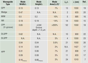
Combining dielectric and plasmonic waveguide principles also has attracted a lot of attention from researchers. For example, a dielectric strip placed on a metal plane yields plasmonic confinement perpendicular to the surface and dielectric confinement parallel to the metal. While these so-called dielectric loaded SPP waveguides exhibit high optical confinement, their propagation lengths are essentially similar to those of SPPs on a flat metal-dielectric interface (Figure 2c).Reference Steinberger, Hohenau, Ditlbacher, Stepanov, Drezet, Aussenegg, Leitner and Krenn22–Reference Briggs, Grandidier, Burgos, Feigenbaum and Atwater24 However, we note that a general design-limiting consideration for dielectric-plasmon-based waveguides is that the propagation loss of SPPs increases with the cubed refractive index of the adjacent dielectric. Employing higher refractive index materials to form a dielectric waveguide therefore increases losses, a problem also exhibited by all plasmonic waveguides that utilize a single dielectric material. When incorporating semiconductor materials, which have the highest refractive indices of all transparent materials at optical frequencies, losses become prohibitive. However, this design can be improved upon significantly when the dielectric core is brought into close proximity to a metal layer but is kept separated by a nanometer thin gap. The resulting optical mode is a hybrid plasmon polariton (HPP), which pulls the optical mode into the nanometer gap layer.Reference Alam, Meier, Aitchison and Mojahedi25, Reference Oulton, Sorger, Pile, Genov and Zhang26 The HPP waveguide features a deep-subwavelength mode down to about one-tenth of the diffraction limit of light in each lateral direction, yet with reasonable propagation lengths, since only a small amount of the optical field resides in the metal, with a significant portion of the energy being in the low refractive index gap (blue layer in Figure 2g).Reference Sorger, Ye, Oulton, Bartal, Wang and Zhang17, Reference Oulton, Sorger, Pile, Genov and Zhang26 A number of configurations based on this principle have now been proposed and demonstrated, all with excellent confinement and propagation characteristics.Reference Alam, Meier, Aitchison and Mojahedi25–Reference Goykhman, Desiatov and Levy29 When benchmarking the performance of single dielectric plasmonic waveguides, for example a cylindrical IMI nanowire and a cylindrical MIM hole in metal, against the HPP waveguides, the latter exhibits an advantage in terms of propagation length versus achievable optical confinement (Figure 2h).Reference Oulton, Bartal, Pile and Zhang21, Reference Oulton, Sorger, Pile, Genov and Zhang26Table I provides a comparison of the optical mode confinement and propagation length for experimental and theoretical demonstrations of various plasmon waveguide architectures.
Plasmonic waveguide comparison of optical confinement (mode area) and propagation length (L m) from the literature, λ free-space wavelength.

GPP, gap plasmons; Wedge, plasmon polaritons; MIM, metal-insulator-metal; IMI, insulator-metal-insulator; CPP, channel plasmon polariton; DLSPP, dielectric loaded surface plasmon polariton; HPP, hybrid plasmon polariton; N.A., not available.
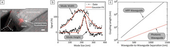
With a number of promising plasmonic waveguides experimentally demonstrating confinement beyond the diffraction limit,Reference Verhagen, Spasenovic, Polman and Kuipers15–Reference Sorger, Ye, Oulton, Bartal, Wang and Zhang17, Reference Pile, Ogawa, Gramotnev, Okamoto, Haraguchi, Fukui and Matsuo20, Reference Steinberger, Hohenau, Ditlbacher, Stepanov, Drezet, Aussenegg, Leitner and Krenn22 we focus our discussions on recent results of the HPP approach, which show promise for mode size scaling with semiconductor materials and hence viability for on-chip opto-electronic PICs (Figure 2g–h and Figure 3). Although the optical fields within the hybrid plasmon architecture are difficult to observe directly, recent experiments have shown how compact they can be. In a recent experiment, laser light was launched into the HPP waveguide and measured from a cut section of the waveguide to reveal the field distribution of a tiny mode (red) “spot” (Figure 3a).Reference Sorger, Ye, Oulton, Bartal, Wang and Zhang17 The mode size here is about 50 × 60 nm2 corresponding to just 3% of the diffraction limited area. The optical wavelength of the laser beam illuminating the waveguide was λillumination at 633 nm. To achieve this result, we used near-field scanning optical microscopy to map the electric field distribution near the output slice through the structure, which was created using focused-ion-beam milling. In order to explore the HPP waveguide’s potential as a spectral broadband interconnect, these waveguides were tested by launching beams with wavelengths ranging from 633 to 1427 nm. For instance, Figure 3b shows the mode height and width of the waveguide excited with an (infrared) IR excitation wavelength of 1427 nm, resulting in a mode height and width of 65 and 210 nm, respectively, which are 0.04 and 0.14 times the diffraction limit (λ2/4), where λ is the free-space wavelength. These results highlight the broadband strong optical confinement of the HPP mode, which originates from the non-resonant waveguide design.Reference Sorger, Ye, Oulton, Bartal, Wang and Zhang17, Reference Oulton, Sorger, Pile, Genov and Zhang26 For passive optical interconnects, where bits of information are simply routed but not actively switched, two criteria are of fundamental importance: first the optical waveguide mode size, which also influences the bending radii and circuit compactness, and second the lateral waveguide-to-waveguide packing density (i.e., the pitch between two waveguides or photonic components without risking crosstalk). Regarding the latter, the HPP waveguide experiences reduced crosstalk due to the strong optical confinement, both vertically (z) and horizontally (x) (Figure 3a–b). For example, Figure 3c shows simulation results of the coupling length defined as the length required for a 50% energy transfer between two identical waveguides; this coupling length between two neighboring hybrid plasmonic waveguides is much larger compared to the dielectric case, here silicon-on-insulator (SOI)Reference Bogaerts, Baets, Dumon, Wiaux, Beckx, Taillaert, Luyssaert, Van Campenhout, Bienstman and Van Thourhout30 waveguides, suggesting a clear reduction in crosstalk for closely spaced waveguides as compared to the pure dielectric case.
Details of the hybrid plasmon polariton (HPP) waveguide.Reference Sorger, Ye, Oulton, Bartal, Wang and Zhang17, Reference Oulton, Sorger, Pile, Genov and Zhang26 (a) Experimental results for mapping the mode size of the HPP mode via near-field-optical spectroscopy (NSOM) overlaid with a scanning electron microscopy micrograph show the tiny waveguide mode as a red spot at the end of the waveguide. Illumination via a laser beam from the bottom of the substrate; λ = 633 nm, scale bar = 100 nm. (b) Experimental mode area resulting in a deep subwavelength mode height (λ/25) and width (λ/7), respectively (full width at half maximum were taken, λ = 1427 nm). (c) Coupling length of the hybrid waveguide benchmarked against pure dielectric waveguides highlighting dense integration possibility. The much weaker field overlaps between nearby hybrid plasmon waveguides and leads to a much longer coupling length, greatly reducing cross-talk. Waveguide cores (height x width) = 250 x 250 nm2. Simulation material indices and optical wavelength (λ): waveguide-core index = 3.5, cladding index = 1, metal index from Reference 31, oxide index = 1.48, λ = 1550 nm.

Plasmonic light sources
Nanoscale plasmon lasers are a potential solution to the challenge to find suitable surface plasmon sources for ultra-compact plasmonic circuits.Reference Sorger and Zhang32, Reference Ma, Oulton, Sorger and Zhang33 Surface plasmon lasers operate by amplification of surface plasmons instead of light, and consequently show distinct operation features compared to classical lasers; the strongly confined electromagnetic fields within a plasmonic laser cavity allow for extremely compact devices, which have been shown to dramatically enhance the spontaneous emission rate due to the Purcell effect, which quantifies the enhancement of the spontaneous emission rate of an emitter relative to its free-space value.Reference Genov, Oulton, Bartal and Zhang34–Reference Stockman36 In particular, this Purcell effect can be enormous in low-dimensional plasmonic nanostructures due to an anomalous scaling with frequency.Reference Genov, Oulton, Bartal and Zhang34 This capability to enhance all light matter interactions inside the laser can lead to exceptionally fast response times even at long wavelengths, away from the surface plasmon resonance.Reference Genov, Oulton, Bartal and Zhang34, Reference Stockman36 Furthermore, the Purcell enhancement can drastically modify the build-up of inversion and stimulated emission (i.e., population inversion) into the dominant laser mode, most notably through a high spontaneous emission factor, β-factor, which is the ratio of spontaneous emission coupled to the laser mode, compared to all the other modes. Significantly, enhancing β reduces the onset of stimulated emission for lasing, which potentially enables low thresholds despite the high losses of metal-dielectric nanostructures.Reference Bjork and Yamamoto37, Reference Oulton, Sorger, Zentgraf, Ma, Gladden, Dai, Bartal and Zhang38 While the potential for low thresholds has attracted much attention, plasmon lasers currently still have significant thresholds owing to the high intrinsic ohmic loss of metals.Reference Sorger and Zhang32, Reference Ma, Oulton, Sorger and Zhang33
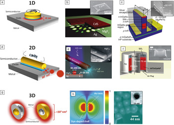
We have discussed how metals can confine light in one or two dimensions using either electron oscillations to store optical energy or surface charge to generate a capacitive confinement effect. To construct a laser, however, a feedback mechanism must be provided, which can be realized by a cavity. A number of breakthroughs in plasmon lasers have provided for a range of devices that use plasmonic confinement with various dimensionality (Figure 4).Reference Sorger and Zhang32–Reference Genov, Oulton, Bartal and Zhang34 One-dimensional plasmonic confinement lasers (Figure 4a) are typically composed of either a square- or circle-shaped cavity relying on a whispering-gallery mode type resonator, typically a circular or hemispherical enclosure featuring total internal reflection (Figure 4b)Reference Ma, Oulton, Sorger, Bartal and Zhang39, Reference Kwon, Kang, Seassal, Kim, Regreny, Lee, Lieber and Park40 or a Fabry–Pérot type resonatorReference Hill, Marell, Leong, Smalbrugge, Zhu, Sun, Veldhoven, Geluk, Karouta, Oei, Nötzel, Ning and Smit41 (Figure 4c). Plasmonic waveguides, such as a semiconductor nanowire, can provide laser gain in a waveguide geometry, for instance, deploying the HPP geometry, which offers strong two-dimensional optical confinement (Figure 4d), can achieve laser action in a Fabry–Pérot type configuration (Figure 4e)Reference Sorger and Zhang32, Reference Oulton, Sorger, Zentgraf, Ma, Gladden, Dai, Bartal and Zhang38 or in a coaxial cavity type (Figure 4f).Reference Khajavikhan, Simic, Katz, Lee, Slutsky, Mizrahi, Lomakin and Fainman42 While these aforementioned cavity configurations provide the necessary feedback for laser action, they cannot be reduced in size in the unbound dimensions beyond the diffraction limit. In order to reduce the laser size below this fundamental limit, one solution is to raise the operation frequency to the surface plasmon frequency. An ultimate nanolaser with a full 3D optical confinement considerably smaller than the wavelength can have a spherical design (Figure 4g). Here two design options are conceivable; either the gain material is in the center surrounded by a metal shell defining the cavity, or the inverse is also possible. Although the latter configuration has been experimentally demonstrated in solution with dye molecules as the gain medium (Figure 4h),Reference Noginov, Zhu, Belgrave, Bakker, Shalaev, Narimanov, Stout, Herz, Suteewong and Wiesner43 this configuration awaits follow-up work, especially in the solid-state regime with semiconductor gain materials, before this strong scaling potential can be exploited for PIC technology.
Plasmon nanolasers with different levels of optical confinement beyond the diffraction limit of light. (a–c) 1D plasmonic optical confinement. (b) Plasmon nanolaser featuring an in-plane cavity and total internal reflection of the resonating mode.Reference Ma, Oulton, Sorger, Bartal and Zhang39, Reference Kwon, Kang, Seassal, Kim, Regreny, Lee, Lieber and Park40 (c) Fabry–Pérot type plasmon laser as a wall-like post.Reference Hill, Marell, Leong, Smalbrugge, Zhu, Sun, Veldhoven, Geluk, Karouta, Oei, Nötzel, Ning and Smit41 (d–f) 2D plasmon optical confinement showing (e) a Fabry-Perot type resonator utilizing the HPP modeReference Oulton, Sorger, Zentgraf, Ma, Gladden, Dai, Bartal and Zhang38 and (f) a coaxial type resonator.Reference Khajavikhan, Simic, Katz, Lee, Slutsky, Mizrahi, Lomakin and Fainman42 (g) Two possible configurations of a spatially localized resonator featuring 3D optical confinement. (h) Localized plasmon laser demonstration utilizing a (14 nm) gold core surrounded by an Oregon Green (OG 488 nm) dye-doped silica shell. The left panel showing the electric field intensity (unity normalized) of the particle resonator indicates a strongly localized field at the metal particle (red area).Reference Noginov, Zhu, Belgrave, Bakker, Shalaev, Narimanov, Stout, Herz, Suteewong and Wiesner43

A natural challenge for all types of plasmon lasers is to couple the lasing signal efficiently into an on-chip waveguide, due to both metal enclosures associated with the plasmonic confinementReference Kwon, Kang, Seassal, Kim, Regreny, Lee, Lieber and Park40–Reference Khajavikhan, Simic, Katz, Lee, Slutsky, Mizrahi, Lomakin and Fainman42 and a mismatch in the speed of waves inside and outside the laser cavity. If the cavity feedback is too strong, only a small amount of useful light will escape the cavity before being absorbed by the metal regions; if the feedback is too weak, the laser threshold becomes unmanageable. The most plausible PIC laser solutions must therefore allow for highly integrated waveguide-to-laser designs. Most importantly, in addition to strong coupling to the on-chip waveguide, coupling to external radiation and non-radiative loss due to the metal should be minimized. A promising design that provides such balance of the various loss channels is achieved by crossing a metal strip with a thin semiconductor nanobelt, creating a waveguide-integrated nanolaser cavity at the crossing point that allows the coupling of laser emission efficiently (>70%) into the semiconductor waveguide.Reference Ma, Yin, Oulton, Sorger and Xiang44
A remaining challenge for this new class of laser is electrical injection under ambient conditions, which is essential for on-chip integration with electrical data input. In particular, challenges arise from the small design window in optimizing both optical and electrical constraints, leaving the optical laser mode and the loss balance mostly undisturbed. However, the metals needed to create plasmon lasers that can carry electrical drive current confine the optical mode and act as a heat sink. Furthermore, the small laser cavity dimensions, and hence high optical mirror and intrinsic metal ohmic losses, impose challenges for plasmon nanolaser operation at room temperature. However, recently a nano-square laser cavity configuration (Figure 4b) has achieved room temperature operation.Reference Ma, Oulton, Sorger, Bartal and Zhang39 This design features strong confinement while simultaneously having low metal loss by employing a hybrid plasmonic waveguide design and also exhibits low radiation loss due to total internal reflection of HPPs. Additional plasmon laser design challenges originate when direct bandgap semiconductors with high gain such as III–V and II–VI compound semiconductors are employed, calling for a hybrid plasmon approach that limits cavity options. The problem is that insulating regions must be used where light interacts most strongly with the metal to ensure no electrical shorting, which in turn prohibits electrical injection. For this reason, most electrically injected metal-based lasers do not utilize plasmonic modes, which bind to the high loss metallic regions, but photonic modes reside in low loss dielectric regions and provide no downscaling of the optical mode size beyond the diffraction limit.Reference Ding, Liu, Yin, Wang, Liu, Hill, Marell, van Veldhoven, Nötzel and Ning45 The cavity of a plasmonic laser requires the smallest possible losses from the metal calling for minimizing the imaginary part of the dielectric function. The best material choices for the gain therefore are the direct bandgap semiconductors such as many III–V and II–VI compound semiconductors. Regarding the choice of the metal, silver and gold thus far show the lowest metal loss, although it is still high.Reference West, Ishii, Naik, Emani, Shalaev and Boltasseva46–Reference Boltasseva and Atwater48 Furthermore, for effective electrical pumping of these lasers, controlling the doping level of semiconductor nanostructures precisely is still part of ongoing research; however, some progress has been made with monolayer doping materials followed by rapid-thermal-annealing.Reference Ho, Yerushalmi, Jacobson, Fan, Alley and Javey49, Reference Ho, Yerushalmi, Smith, Majhi, Bennett, Halim, Faifer and Javey50
Optical modulation
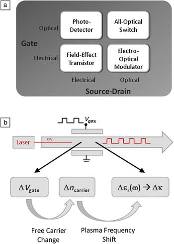
A fundamental function of PICs and the emerging nanoscale plasmonic counterparts is to encode (i.e., switch) and route data. Related to switching, there are generally four options when electrical and optical processes are to be considered, classified by the 2 × 2 matrix shown in Figure 5a. The matrix assumes that we wish to modulate either an electronic or optical signal by some form of either an electronic or optical gate. For instance, transistors are well-known examples in which an electrical signal can be switched by an electrical gate.Reference Chau, Datta, Doczy, Doyle, Jin, Kavalieros, Majumdar, Metz and Radosavljevic51 The same electrical signal switched by an optical gate can be referred to as an optical transistor, which resembles a photodetector.Reference Miller52, Reference Okyay, Pethe, Kuzum, Latif, Miller and Saraswat53 The remaining functions rely on non-linear optics and currently are very weak effects requiring long interaction lengths and/or high optical power. For example, an all-optical switch, where an optical signal is encoded by an optical gate, requires high power laser beams to achieve the necessary gating effect.Reference Sasaki, Sasaki and Furukawa54–Reference Dawlaty, Rana and Schaff56 The last approach is to switch an optical signal electrically, which is the function of an electro-optic modulator (EOM).Reference Sincerbox and Gordon57–Reference Jung, Yee and Kuhn60 This is a fundamental element of optical interconnects, as it is the conversion point between electronic and optical information. The alternative approach to EOMs, direct modulation of the laser, is generally avoided in on-chip circuit designs due to the interference of laser dynamics with the modulated signal, causing unstable signals.Reference Paniccia, Krutul and Koehl2, Reference Welch, Kish, Nagarajan, Joyner, Schneider, Dominic, Mitchell, Grubb, Chiang, Perkins and Nilsson3
Logic and data switching for integrated circuits. (a) Generally there are four possibilities for logic using optics and electronics. For photonic integrated circuits (PICs),Reference Welch, Kish, Nagarajan, Joyner, Schneider, Dominic, Mitchell, Grubb, Chiang, Perkins and Nilsson3 three options are of interest; electrical data can be encoded onto an optical beam via electro-optic modulator. An all-optical approach has high potential for ultra-fast switching. When PIC elements are combined with electronic ICs, a photonic transistor is of interest that essentially is an optically gated electrical transistor or a photodetector. (b) Of particular interest for PICs is the electro-optic modulator, since it allows for stable laser operation and standardized optical power levels inside the circuit.Reference Dionne, Diest, Sweatlock and Atwater5, Reference Sorger, Lanzillotti-Kimura, Ma and Zhang7 The schematic shows how a voltage (V gate) induced free carrier change (n carrier) leads to a shift of the active material’s relative permittivity (Δεr(ω), with ω being the angular frequency) and consequently to a shift in the real and imaginary part (Δκ) of the propagating modal index. With these two methods, either a phaseReference Liu, Jones, Liao, Samara-Rubio, Rubin, Cohen, Nicolaescu and Paniccia62 or an absorption modulatorReference Dionne, Diest, Sweatlock and Atwater5, Reference Sorger, Lanzillotti-Kimura, Ma and Zhang7 (shown here) can be designed.

Figure 5b schematically shows a commonly used EOM approach; a continuous wave (cw) laser beam enters a parallel-plate capacitor, and the data carrying voltage applied to the capacitor encodes data onto the cw optical laser beam by changing the refractive index of the optical mode. Utilizing this change of the real or imaginary part of the refractive index, either an interferometer-type phase modulator (e.g., Mach-Zender) or a linear electro-absorption modulator can be designed, respectively. Typical active materials for phase modulators are lithium niobate via shifting the optical non-linear coefficient, which refers to a non-linear response of a material’s polarization as a function of electric field intensity,Reference Taylor, Taylor and Bauer61 InP quantum wells,Reference Welch, Kish, Nagarajan, Joyner, Schneider, Dominic, Mitchell, Grubb, Chiang, Perkins and Nilsson3 free carrier modulation of silicon,Reference Liu, Jones, Liao, Samara-Rubio, Rubin, Cohen, Nicolaescu and Paniccia62–Reference Reed, Mashanovich, Gardes and Thomson65 and highly non-linear polymers.Reference Tian, Chen, Haller, Tucker, Ka, Luo, Huang and Jen66 Absorption modulators have been realized using carrier modulation of silicon,Reference Dionne, Diest, Sweatlock and Atwater5 graphene,Reference Liu, Bin, Avila, Zentgraf, Ju, Wang and Zhang67 and indium tin oxide (ITO).Reference Sorger, Lanzillotti-Kimura, Ma and Zhang7 ITO belongs to the class of transparent conducting oxides that can be doped depending on the oxygen vacancy and interstitial metal dopant concentrations.Reference Gordon68, Reference Hamberg and Granqvist69 Furthermore, the carrier density can be greatly tuned when ITO becomes part of a metal-oxide-semiconductor (MOS)-capacitor design upon applying an electrical bias, which can be used to modulate the optical signal.Reference Sorger, Lanzillotti-Kimura, Ma and Zhang7, Reference Feigenbaum, Diest and Atwater70
The opportunity for plasmonic electro-optic modulation arises from the enhanced interaction of the light beam with the active material related to modulation. With the emerging technology of silicon photonics for PICs, high extinction ratio EOMs have been demonstrated in silicon-on-insulator waveguide designs by increasing or decreasing the free carrier density in the silicon waveguide core.Reference Liu, Jones, Liao, Samara-Rubio, Rubin, Cohen, Nicolaescu and Paniccia62–Reference Green, Rooks, Sekaric and Vlasov64 However, to achieve high modulation depth (>10 dB), not only significant voltages (∼10 V) are required, but also large device sizes (typical mm to cm) to accumulate the necessary 180° phase change.Reference Liu, Jones, Liao, Samara-Rubio, Rubin, Cohen, Nicolaescu and Paniccia62 The wafer footprint can be reduced to tens of micrometers by deploying a ring-resonator, but with drastically reduced optical bandwidth to the sub-nanometer range and temperature instabilities associated with high quality cavities.Reference Xu, Schmidt, Pradhan and Lipson63
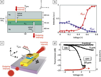
Absorption modulators have been realized using novel materials such as graphene, which show improved extinction ratios over silicon-only free carrier modulators due to the graphene’s potential to change its absorption as a function of applied voltage (i.e., via shifting the Dirac-Point, the position in reciprocal space where the six Brillouin corners meet).Reference Liu, Bin, Avila, Zentgraf, Ju, Wang and Zhang67 Plasmonic EOMs, in particular absorption types, have been proposedReference Cai, White and Brongersma71 and demonstrated,Reference Dionne, Diest, Sweatlock and Atwater5, Reference Sorger, Lanzillotti-Kimura, Ma and Zhang7, Reference MacDonald, Sámson, Stockman and Zheludev72 indicating a promising path for light-matter enhanced switches. The first plasmonic waveguide-based modulator utilized the MIM waveguide geometry forming a capacitor (Figure 6a).Reference Dionne, Diest, Sweatlock and Atwater5 The internal device mechanism is to change the refractive index of a sandwiched silicon layer between the two metal layers, forming an electrical capacitor. Applying a voltage bias between the metal and the silicon leads to carrier accumulation and a shift of the silicon’s optical dispersion. The device geometry (Figure 6a) features a very compact design (length = 2.2 μm) and exhibits efficient modulation depths of 10 dB for ∼1 volt of applied bias at telecommunication wavelengths (1.3–1.55 μm) (Figure 6b).Reference Dionne, Diest, Sweatlock and Atwater5 While the demonstrated insertion loss in the ON-state (no voltage) was rather high (–20 dB), the free space-to-MIM waveguide coupler can be optimized to reduce this high loss. A different design demonstrated a SOI waveguide-integrated electro-absorption EOM featuring the HPP mode. This compact (3-λ-long) EOM is based on a silicon waveguide and supports a MOS-type HPP mode (Figure 6c).Reference Sorger, Lanzillotti-Kimura, Ma and Zhang7 The maximum of the electric field intensity resides in a 10-nm-thin layer overlapping with the active material, ITO. A significant amount of light remains in the silicon core, which allows for extremely low on-chip insertion losses in the ON-state of only –1 dB for a 3-λ-long device,Reference Sorger, Lanzillotti-Kimura, Ma and Zhang7 which is significantly lower than non-plasmonic architectures because of a much shorter device length and low impedance mismatch for the optical mode to propagate through the device.Reference Sorger, Lanzillotti-Kimura, Ma and Zhang7, Reference Liu, Jones, Liao, Samara-Rubio, Rubin, Cohen, Nicolaescu and Paniccia62 The device’s switching mechanism originates from a formed accumulation layer at the ITO-SiO2 interface, which alters the free carrier absorption and thus converts the low-loss ITO in the ON-state to a high-loss metal-like material in the OFF-state (voltage applied). Design synergies are generated through utilizing the metal pad to create the plasmonic optical mode that also serves as an electrical contact. The modulation depth of this modulator exceeds 1 dB/μm, which is remarkable compared to SOI devices that operate as a phase shifterReference Liu, Jones, Liao, Samara-Rubio, Rubin, Cohen, Nicolaescu and Paniccia62 (Figure 6d). Since the deployed HPP mode is broadband in nature,Reference Sorger, Ye, Oulton, Bartal, Wang and Zhang17 a similar broadband operation range is expected and was demonstrated (i.e., 1000 nm),Reference Sorger, Lanzillotti-Kimura, Ma and Zhang7 implying design flexibility with respect to wavelength-division-multiplexedReference Kaminow, Doerr, Dragone, Koch, Koren, Saleh, Kirby, Ozveren, Schofield, Thomas, Barry, Castagnozzi, Chan, Hemenway, Marquis, Parikh, Stevens, Swanson, Finn and Gallager74 circuitries. Furthermore, given the small device size of these two electro-optic modulators,Reference Xu, Schmidt, Pradhan and Lipson63–Reference Reed, Mashanovich, Gardes and Thomson65 the resulting capacitance and resistance are limited, in other words, RC delay time and hence upper limit of the operation speed can be estimated to be hundreds of GHz with a low power consumption of only a few to tens of fJ/bit, an improvement of close to three orders of magnitude over non-plasmonic devices.Reference Dionne, Diest, Sweatlock and Atwater5, Reference Sorger, Lanzillotti-Kimura, Ma and Zhang7 This low power consumption is a necessity for future optical communication linksReference Miller75 and exemplifies the potential of plasmonics in PICs.
Plasmonic electro-optic modulation. (a) Cross-sectional schematic of a silicon field-effect plasmonic modulator.Reference Dionne, Diest, Sweatlock and Atwater5 Subwavelength slits milled through the Ag cladding form the optical source and drain, through which light is coupled into and out of the modulator. (b) Optical drain intensity as a function of gate bias (V gate) for two source—drain separations d ds (distance, d ds1 = 2.2 μm and d ds2 = 7.0 μm) at a wavelength λ = 1.55 μm.Reference Dionne, Diest, Sweatlock and Atwater5 The onset of significant modulation occurs for voltages of approximately 0.5 V and saturates of approximately 0.7 V. (c) Schematic of a waveguide-integrated, compact, silicon-based nanophotonic modulator.Reference Sorger, Lanzillotti-Kimura, Ma and Zhang7 The metal-oxide-semiconductor (MOS) design features a plasmonic hybrid plasmon polariton mode, which concentrates the mode’s electric field and allows for good modal overlap with an active indium tin oxide (ITO) layer. (d) The modulator performance yields a record-high 1dB/μm extinction ratio and is a direct result of the plasmonic MOS mode and the active material’s (ITO) ability to alter its optical loss.Reference Sorger, Lanzillotti-Kimura, Ma and Zhang7 Increasing the device length results in stronger modulation down to –5 dB and –20 dB for 5 (black triangles) and 20 μm (black dots) long devices, respectively. No modulation was observed for reversed bias polarity when the ITO layer was omitted in control devices (black squares). The MOS capacitor operation is indirectly verified by a low leakage current (red dots) of about half a nano-ampere.

Photodetection
In a plasmonic PIC following the generation, routing, and modulation of surface plasmons, these data packages have to be converted from the optical into the electrical domain, which can be realized via a photodetector. Even for photonic-plasmonic hybrid circuits, there are a number of important reasons why such an integrated plasmonic detector provides advantages over conventional detectors. Similar to the surface plasmon source, waveguide, and modulation, the plasmonic detector can be of nanoscale dimensions, offering multiple advantages such as (1) higher integration densities, (2) low device capacitance for fast transit times, allowing for higher bandwidth operation, and (3) reduced energy to operate, owing to enhanced light matter interactions. When shrinking the detector’s size, there can be a clear reduction in its response time; however, the reduced absorption of the medium (typically a semiconductor) limits the sensitivity, defined as the minimum light intensity, and responsivity (i.e., gain), defined as photocurrent per light intensity. With emerging active plasmonics, plasmonic detectors have the potential to counteract this size down-scaling absorption degradation by enhancing the material absorption similar to the manner in which spontaneous emission is enhanced by the Purcell effect in plasmon nanolasers.Reference Sorger and Zhang32, Reference Ma, Oulton, Sorger and Zhang33, Reference Oulton, Sorger, Zentgraf, Ma, Gladden, Dai, Bartal and Zhang38, Reference Ma, Oulton, Sorger, Bartal and Zhang39
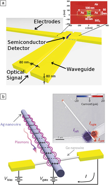
Toward achieving strong photo-absorption, the local density of states (LDOS) inside the absorbing semiconductor region should be enhanced, however without introducing unfavorable quenching channels.Reference Mallick, Sergeant, Agrawal, Lee and Peumans76, Reference Callahan, Munday and Atwater77 Plasmon-based photodetection of PICs can be categorized into two scenarios: the optical data arrive (1) in a diffraction limited waveguide, such as in silicon photonics or (2) in a subwavelength, as in the plasmonic case. In the former, the challenge is to first impedance-mode-match the large photonic mode to a tiny plasmonic one before it can be absorbed and hence detected. The field of nanofocusing explores various approaches for concentrating light into deep subwavelength volumes for photodetection such as the use of apertures to confine optical beams,Reference Tang, Miller, Okyay, Matteo, Yuen, Saraswat and Hesselink78, Reference Tang, Latif and Miller79 nanoantennas,Reference Tang, Kocabas, Latif, Okyay, Ly-Gagnon, Saraswat and Miller80 and tapered nanometallic waveguides.Reference Verhagen, Spasenovic, Polman and Kuipers15, Reference Dionne, Lezec and Atwater16 With nanoantennas being helpful for light harvesting, photodiodes convert light into a photocurrent. The Halas group has recently shown that these two independent functions can be combined into one device, where resonant plasmons created by a plasmon nanoantenna absorbing photons create “hot” electrons, which can tunnel across a Schottky-barrier, producing a photocurrent.Reference Knight, Sobhani, Nordlander and Halas81 For case (2), where the optical data carrying the waveguide’s mode size is of the same order as the nanoscale absorber of the detector, no impedance transformer is needed. Figure 6a highlights this scenario for an integrated MIM slot-waveguide, where the deep-subwavelength data-carrying mode is converted into electrical data.Reference Ly-Gagnon, Balram, White, Wahl, Brongersma and Miller82, Reference Gu, Bai and Li83 LDOS-enhanced absorption can, for instance, be achieved by utilizing the electric field enhancement of metallic nanoparticles in combination with highly absorbing quantum dots, thus boosting sensitivity and responsivity.Reference Hsu, Chang, Chen, Kuo, Chen, Pei and Li84 In recent work, graphene, in conjunction with sheets of quantum dots, was utilized to produce a giant photocurrent gain (108 A/W) and simultaneously sensitivities down to tens of fW of optical power.Reference Konstantatos, Badioli, Gaudreau, Osmond, Bernechea, Garcia de Arquer, Gatti and Koppens85 However, this device requires a voltage reset step, which slows the device response time down to 10 msec. Furthermore, Falk et al. demonstrated all-electrical plasmon detection at the nanoscale (Figure 6b).Reference Falk, Koppens, Yu, Kang, de Leon Snapp, Akimov, Jo, Lukin and Park86 This plasmon detector is based on the near-field coupling between guided plasmons and a nanowire field-effect-transistor. Gating the transistor can increase the number of electrons per plasmon from 0.1 up to 50.Reference Falk, Koppens, Yu, Kang, de Leon Snapp, Akimov, Jo, Lukin and Park86 However, the plasmon detection sensitivity could be improved by deploying an avalanche photodiode potentially allowing for electrical detection down to the single plasmon level. Regarding material choices, an ideal material for photodetection in the telecommunication frequency band is germanium, since it provides high absorption (∼104 cm–1) and can readily be integrated with silicon technology. Looking ahead at power consumption and speed performance requirements of future plasmonic circuits, the nanoscale dimensions of plasmonic photodetectors automatically lead to capacitances as low as sub fF, an improvement of up to two orders of magnitude.Reference Ly-Gagnon, Balram, White, Wahl, Brongersma and Miller82 Hence if the contact resistance can be made on the order of hundreds of ohms, the resulting device operating speed shall exceed THz, which would denote a leap forward from the current 40 GHz.Reference Assefa, Xia and Vlasov87, Reference Kang, Liu, Morse, Paniccia, Zadka, Litski, Sarid, Pauchard, Kuo, Chen, Zaoui, Bowers, Beling, McIntosh, Zheng and Campbell88 In addition, similar to the light sources and modulators we have discussed before, plasmon waveguide metal bars can be used elegantly as electrical connectors carrying electrical data away from the absorbing semiconductor, thus allowing for a densely integrated circuit design (Figure 7a).
Photodetection schemes for plasmonic integrated circuits. (a) A tiny light absorbing semiconductor particle (e.g., germanium (Ge) for circuits operating at telecommunication frequencies) is placed at the end of a plasmonic waveguide for local density of states enhanced absorption of the incoming optical data, creating electron-hole pairs. These carriers can be extracted via electrical leads made from the same surface plasmon polariton waveguide, allowing for a densely integrated design. For low power consumption and high speed circuits, the goal for the detector is to reduce its capacitance by shrinking its size into the nanoscale.Reference Ly-Gagnon, Balram, White, Wahl, Brongersma and Miller82 Inset, high field intensity (|E|2) of the absorber region. The colors show the intensity (magnitude of the Poynting vector) in the y-direction, and the arrows indicate the direction and magnitude of the tangential electric field (Ex and Ez). (b) Crossing a metal and semiconductor nanowire sets up a Schottky-junction, back-gated transistor, which can be used for sensitive detection of single surface plasmons. Inset, scanning electron micrograph of the main panel, overlaid with the photocurrent through the Ge nanowire as a function of laser position. Laser power P = 2.0 μW, wavelength λ = 532 nm, V bias = 0, V gate = 0, I = photocurrent, and I SPP the photocurrent portion of the surface plasmon polariton, I left the portion of the current being collected on the left, and I right the current being collected on the right.Reference Falk, Koppens, Yu, Kang, de Leon Snapp, Akimov, Jo, Lukin and Park86

Power considerations
The two aforementioned advantages of plasmonic integrated circuits, namely dense integration and high performance (i.e., speed), might not be their ultimate selling points. In fact, it might be power consumption and efficiency (i.e., the number of photons needed to transmit a bit of information) that provide the necessary business case for these circuits to become commercialized. The rationale behind such outlook is based on reports claiming that the amount of energy used for our data-hungry internet, mobile applications, and server farms is doubling about every 19 months.89 To make the case even more dramatic, already 2% of all electricity in the United States is used for data centers.Reference Markoff90
Data communication is so power hungry because the energy per bit required for communication is about three orders of magnitude larger than the energy per bit required for logic and storage.Reference Yablonovitch91 In the optical domain, this translates to an energy amount of 100,000 k BT, where k B is the Boltzmann constant, and T the operation temperature. Thus, a natural aim of future circuits, whether they are electric, photonic, plasmonic, or hybrids thereof, is to reduce the energy per bit. For PICs, this means reducing the photons per bit, which brings us to the question of what building block of plasmonic PICs might be the limiting factor? It is arguable that noise limits (i.e., shot and Johnson noise, which originate from the discrete electron transport, and thermal noise, respectively) of the photodetector will dictate this minimal photon per bit function of future PICs. A fundamental analysis of the shot and Johnson noise of photodetectors reveals an optical power limit for the photodetector corresponding to about 4 k BT times the data bandwidth, suggestive of orders of magnitude scaling potential compared to current light-level standards of the order of several milliwatts of optical power.Reference Yablonovitch91 And even though the energy per bit function is expected to fall in the long run, it might take a while before all-plasmonic circuits are considered by the industry. As an interim step, plasmonics could become important in hybrid circuits consisting of passive photonic elements and active plasmonic switching and light-manipulation devices. With the current trend for photonic PICs to deliver more bandwidth by adding more parallel channels and increasing the data rate per channel,92 the optical intensities in the waveguides can lead to two-photon absorption, increasing free carrier absorption, which reduces the optical intensity in the circuit and consequently adds thermal losses. While these parasitic effects are unavoidable, optically generated electrical carriers could be harvested through an on-chip photovoltaic effect.Reference Jalali, Fathpour and Tsia93 The recovered electricity could then be fed back into driving other electronic components in the circuit, thus saving overall energy.
Conclusion
Ongoing trends for more computing power and faster communications make a compelling case for photonic integrated circuits employing plasmonic elements. These novel on-chip platforms are promising candidates to deliver high performance circuits in terms of saving material and wafer real estate, as well as energy, and to deliver high data bandwidth performance. Significant progress on individual building blocks points to the potential of such high performance circuits, mainly owing to small device footprints, novel physical effects, and smart integration by exploiting synergies between optics and electronics—a natural advantage of plasmonics (i.e., metal optics). The driving force behind such progress lies in material, fabrication, and design developments as well as demand side effects, such as the desire for ever-increased computing power and data connectivity. However, there are still opportunities for research, such as solving the challenge of efficient coupling optical fields below the diffraction limit of light between devices, the loss penalty of plasmonics, and seamless integration of multiple components into circuits.