
Silicon (Si) nanostructures are possible to be produced as zero-dimensional nanoparticles (NPs), one-dimensional (1D) nanowires (NWs), and two-dimensional thin films. Si-based nanostructures exhibit better optical, electrical, and mechanical properties compared with bulk Si. Due to the fascinating properties exhibited by nanomaterials, they have gained interest in nanoscale electronic devices, mesoscopic research, and miniaturization of devices, while enhancing efficiency and reducing costs. Silicon NWs (SiNWs) have gained their importance in photovoltaics, memory devices, battery applications, photo sensors, biosensors, and many more. Similar to realization of SiNWs for many electronic applications, Si–SiO x core–shell NWs have gained interest in transistors, batteries, and solar cells.[ Reference Cui, Ruffo, Chan, Peng and Cui 1 , Reference Lim, Lee, Yang, Kim, Jeong, Park and Shin 2 ] SiO x wrapped SiNW facilitates its use as a cylindrical dielectric layer with a wrapped metal gate that exhibits a reduced consumption of power and a better coupling of gate as compared with planar field effect transistors. The enhancement in the field emission properties of the SiNWs is observed due to the positive electron affinity of 0.6–0.8 eV in Si–SiO x core–shell NWs.[ Reference Nie, Chen, Wu, Wang, Zhang, Fan, Yang, Jiang and Zou 3 ] Si–SiO x core–shell NWs have gained tremendous interest in emerging electronics such as lithium-ion batteries, where the capacity contribution is achieved from core Si and amorphous SiO x accommodates large volume variation during the charge and discharge cycles of a battery. Recently, this was demonstrated by growing 10 nm Si core covered by 50 nm SiO x [ Reference Cui, Ruffo, Chan, Peng and Cui 1 ] and further investigated by altering dimensions of SiO x shell.[ Reference Lim, Lee, Yang, Kim, Jeong, Park and Shin 2 ] Luminescence applications signifying better efficiency with SiO x shell layer compared with hydrogen-passivated NWs.[ Reference Kim, Kim, Shin, Hong, Kim, Kim, Choi, Kim, Elliman and Kim 4 ] SiO x shell acts as an effective passivation layer for low-velocity recombination, enhances the electron transport in SiNWs coated with SiO x due to negative dipole of Si oxide and demonstrating an enhancement in the efficiency of the solar cell.[ Reference Zhang, Sun, Song, Zhu and Lee 5 ] By measuring the surface dipole energy about 0.2 eV produced by SiO covered SiNW that leads to band bending of 170 meV shows potential in enhancing efficiency in solar cells compared with untreated SiNWs.[ Reference Bashouti, Pietsch, Brönstrup, Sivakov, Ristein and Christiansen 6 ] Different phases by phase formation of silicide NWs were recognized by capping NWs with a SiO x shell that provided improved understanding of the growth mechanism.[ Reference Lin, Chen, Xu and Huang 7 ] Due to the high surface defects exhibited by SiNWs, there is a need for a surface passivation before incorporating NWs in electronic devices. High chemical stability and better compatibility without causing any stress to SiNWs, SiO x is the best candidate as a protective shell.[ Reference Nie, Chen, Wu, Wang, Zhang, Fan, Yang, Jiang and Zou 3 ] SiO x covered SiNWs show better absorption in short wavelengths that is low in uncoated SiNWs.[ Reference Baranov, Zamchiy and Khmel 8 ]
To obtain the best performance from SiNWs, the design of 1D Si–SiO x core–shell NW structures is in much demand. Currently, Si–SiO x core–shell NWs are fabricated by thermal evaporation of SiO2 and Si powders,[ Reference Lim, Lee, Yang, Kim, Jeong, Park and Shin 2 ] carbon-assisted growth at 1100 °C,[ Reference Chiew and Cheong 9 ] nickel-mediated growth by plasma-enhanced chemical vapor deposition (PECVD) and horizontal tube furnace at 1100 °C,[ Reference Kim, Kim, Shin, Hong, Kim, Kim, Choi, Kim, Elliman and Kim 4 ] oxide-assisted growth process at 900 °C,[ Reference Zhang, Lifshitz and Lee 10 ] and condensation of SiO vapor on SiNWs during growth at 1300 °C.[ Reference Chiew and Cheong 9 ] However, Si–SiO x NWs obtained by these techniques are not uniform, demand for high temperatures for growth processes, uncontrolled growth processes, some growth techniques utilize the oxidation of the NW to obtain SiO x shell, which consumes few Si atoms from a SiNW. Some growth techniques rely on coating SiNWs with a SiO x layer, which poses a non-uniform coating due to the shadowing effect caused by the overlapped NWs that are touching each other. Primarily, Si–SiO x NWs are demonstrated by the oxide-assisted growth. Several fabrication growth processes including the vapor–solid–solid (VSS), solid–liquid–solid, VSS, and vapor–liquid–solid (VLS) are attractive to produce voluminous NWs by simple process steps. Nevertheless, until now, these methods are used either to produce SiNWs, SiO x NWs or silica NWs.[ Reference Nie, Chen, Wu, Wang, Zhang, Fan, Yang, Jiang and Zou 3 , Reference Zamchiy, Baranov and Khmel 11 – Reference Gabrielyan, Saranti, Manjunatha and Paul 13 ]
This work demonstrates the growth of Si–SiO x NWs simultaneously without additional process steps in large quantities, which are uniform, well defined, and better aligned. This process does not pose problems associated with non-conformal coating due to the shadowing of NWs and allows the optimization and controlled growth with a mature and already available PECVD technique at low temperatures (300 °C). This process allows tailoring of SiO x shell layer thickness and as grown pristine SiNWs protected by a SiO x shell can be extracted by removal of oxide layer (e.g., HF dip) in later fabrication steps for appropriate applications. In situ, simultaneous growth of Si–SiO x NWs in a single step eliminates the contamination of SiNWs from the foreign species that are present in the reactive plasma and the external environment when exposed. Si–SiO x NWs are grown instantaneously in a single pump-down process from reduced metal-oxide NPs (MONPs) in vacuum using a conventional VLS growth process via a PECVD technique. Similar to the growth morphology of SiNWs that are controlled by a metal catalyst in standard VLS process, here the Si–SiO x growth morphology and dimensions of a core and shell is possible to be controlled by optimizing the physiochemical properties of a metal-oxide catalyst such as thermodynamic, the concentration of dissolved atoms, and the size of the catalyst. The presence of SiO x shell precipitating from the initial stage of SiNW growth prevents the growth of the NWs in lateral directions that leads to a controlled diameter of synthesized NWs. A similar growth process can be applied to grow SiNWs passivated with nitrogen (–N) and hydrogen (–H) atoms/molecules in a single in situ fabrication growth process, which eliminates the additional deposition process that is used for the passivation of SiNWs.
Methods
Fluorine-doped tin oxide (FTO)-coated glass and Corning glass-2875 (CG) substrates purchased from Sigma-Aldrich are sequentially cleaned for 15 min in Hellmanex, Acetone, IPA, and DI water in a ultrasonic bath. Later, substrates were dried with N2 gas and annealed at 150 °C in an oven for 30 min. FTO-coated glass substrates were loaded in a PECVD (Oxford instruments-PlasmaLAB, Yatton, Bristol, UK) chamber and pumped down to a base pressure of 7 mTorr. The growth of Si–SiOx core–shell NWs involved the following steps: (1) formation of tin oxide NPs (SnONPs) by heating the substrates at 400 °C in the presence of H2 plasma at a hydrogen flow rate of 100 Sccm and with RF power of 55 mW/cm2 for 3 min under 200 mTorr chamber pressure. (2) Immediately after H2 plasma treatment, the growth of Si–SiO x NWs are obtained by introducing 20 Sccm of SiH4 gas for 30 min while maintaining all other parameters unchanged. A similar NW growth process was performed for CG coated with a thin layer of Tin(II) Acetylacetonate (SnAcAc), which was used to produce SnO2 NPs. The PECVD growth process remained as the same as the one explained earlier except the fact that the temperature was maintained at 300 °C.
Growth of NWs from organic and inorganic compounds of Sn
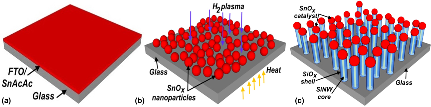
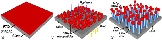
SnONPs are prepared by annealing FTO- and SnAcAc-coated substrates at aforementioned temperatures under H2 plasma treatment. This is useful in removing the surface oxide of SnONPs that mediate the adsorption of Si atoms into SnONPs.[ Reference Misra, Yu, Chen, Foldyna and Roca I Cabarrocas 12 , Reference Tang, Maurice, Chen, Misra, Foldyna, Johnson and Roca i Cabarrocas 14 , Reference Yu, O'Donnell, Foldyna and Roca i Cabarrocas 15 ] In our experiments failing H2 plasma, the growth of NWs is not observed due to inefficiency of Si adsorption posed by the surface oxide layer. It is worth mentioning that H2 plasma helps in the formation of SnONPs and the reduction of the surface oxide layer caused due to the minimization of the energy. The growth of Si–SiO x NWs is similar to the VLS growth process, where SiH4 is dissociated into SiH x radicals, with the help of the elevated temperature and plasma. SiH x radicals deposited on the surface of SnONPs will lead to the adsorption of Si atoms mediated at the surface of the NPs. SnO-assisted growth mechanism is better understood by competing reactions shown by adsorbed Si atoms in the presence of the oxygen atoms in SnONPs that precipitate at solid–liquid (S–L) interface into Si–SiO x NWs (Fig. 1). When the concentration of Si atoms is higher than the equilibrium concentration, drives the precipitation of Si and O atoms at S–L interface to attain minimum free energy in an alloy catalyst.
An illustration of the steps involved in Si–SiO x nanowire growth process. (a) Thin film of FTO and/or SnAcAc coated on CG. (b) Reduction of thin film into SnO nanoparticles when subjected to temperature and H2 plasma treatment. (c) Si core covered with SiO x shell nanowires grown from simultaneous precipitation from a metal compound NPs.

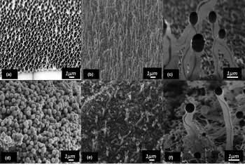
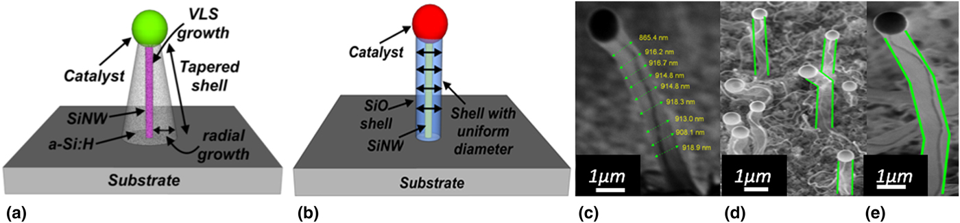
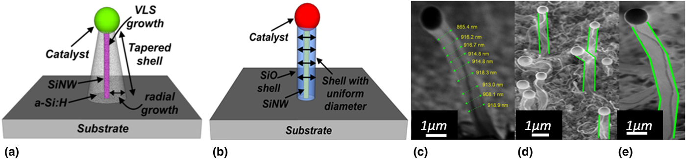
NPs are densely packed but discrete [Fig. 2(a)] and aggregated [Fig. 2(d)] for NPs synthesized from FTO and SnAcAc, respectively. As grown NWs represent dark core region indicating densely arranged Si atoms that could be crystalline enveloped by amorphous matrix formed either by amorphous Si or Si oxide [Figs. 2(c) and 2(f)]. Moreover, the amorphous matrix is not a native oxide of Si core as the native oxide is a few nanometers (<2 nm) and the region here is approximately 400 nm covered in all directions. VLS grown SiNWs via a PECVD process are generally coated by amorphous Si and appear to be tapered [Fig. 3(a)]. However, the NWs grown here are not tapered indicating the absence of a-Si:H shell. A noteworthy fact is that the tapering of a NW is not observed and ascribed to SiO x shell acting as a barrier for sidewall deposition of a-SiH. The formation of SiO x shell is predicted from several mechanisms and narrowed down to a possible mechanism: (1) the simultaneous decomposition of tin oxide from hydrogen plasma that acts as a source of oxygen, which can bind with the surface Si atoms of a SiNW. In this scenario, the catalyst particles size should decrease due to decomposition leading to tapered NWs. NWs are not tapered as seen in Fig. 2. Hence, this might not be a possible growth mechanism. (2) Oxidation of the NWs when exposed to atmosphere, but native oxide is a few nanometers (<2 nm). However, the shell of a NW in this work is approximately 400 nm in radius, suggesting this could not be a possible mechanism. (3) The continuous precipitation of O and Si atoms nucleated in liquid catalyst at liquid–solid (L–S) interface on a substrate is a possible occurrence. The uniform diameter of a shell from bottom to top of a NW [Fig. 3(c)], the presence of a catalyst on top of a NW (Fig. 2) and diameter of a shell that is approximately equal or less than the diameter of a catalyst [Figs. 3(c)–3(e)] provides further evidence to confirm a shell is formed by precipitation from a catalyst to attain minimum free energy and not by any other mechanism.
Si–SiO x nanowire growth process. SEM images showing synthesized SnO nanoparticles from FTO and SnAcAc (a) and (d), respectively. Si–SiO x NWs mediated growth from SnO NPs synthesized from FTO (b) and SnAcAc (e), respectively. High magnification image of few individual nanowires showing core (dark region) covered with a shell (gray region) attributed to SiNW covered with SiO x synthesized from FTO (c) and SnAcAc (f), respectively.

Growth mechanism of SiO x shell. Tapering of nanowire due to deposition of a-Si:H at the sidewall of a NW in a PECVD process (a). SiO x shell covered across SiNW precipitated by SnO NP (b). SEM image of individual nanowires (c–e) with a core and shell along vertical cross-section of a NW.
There are several reports on the use of ITO, FTO, SnO2, and/or In2O3 to obtain In or Sn NPs to grow SiNWs.[ Reference Yu, O'Donnell, Foldyna and Roca i Cabarrocas 15 – Reference Alet, Yu, Patriarche, Palacin and Roca I Cabarrocas 17 ] In contrary, they are used also for the growth of silica (SiO x ) and SnO2 NWs.[ Reference Zamchiy, Baranov and Khmel 11 , Reference Luo, Liang and Jie 18 ] It is shown that, 5 min H2-plasma at temperatures <400 °C, metal NPs are formed. However, this phenomenon is not observed in this work for SiNWs grown from FTO. Conversely, few thin NWs are observed without a shell for NWs grown from SnAcAc along with core–shell NWs that could arise from formation of tiny Sn NPs from complete dissociation of organic molecules attached to Sn atoms. However, the nucleation, supersaturation, and precipitation of Si atoms in metal NPs such as indium, tin, gold, bismuth, and gallium and many more metals are explained and thoroughly studied by many researchers,[ Reference Misra, Yu, Chen, Foldyna and Roca I Cabarrocas 12 ] whose underlying principle is based on the eutectic temperature, the morphology of catalyst, the equilibrium solubility concentration, surface tension, sidewall wetting by catalyst, and the fabrication procedure involved during growth process. In contrast, the core–shell NWs grown here are different with the use of metal-oxide NPs (MONPs) that are used for nucleation and precipitation. Continuous growth is achieved from MONPs due to the simultaneous reduction of the oxide layer promoted from H2 plasma. Thickness of core and shell is possible to be controlled by modifying the diameter of MONPs where the concentration of Sn and O are controlled (Supplementary Fig. S1). Alternatively, H-plasma treatment and temperature could be modified to control the morphology and concentration of species within the MONPs. SiH4 gas flow and RF power density are other options to control thickness of NWs; here control over the amount of Si that get adsorbed, diffused, and precipitated from the particle is achieved.
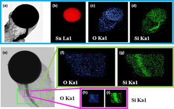
Based on the bright-field STEM contrast image (Fig. 4) with EDS elemental mapping, it is clear that Si core and SiO x shell is formed from the precipitation of corresponding atoms at the middle and the outer regions of a catalyst, respectively. The alloy catalyst of a NW has Sn, O, and Si atoms, which show a potential of precipitating Si and O atoms to grow NWs. NWs did not show any trace of Sn atoms with a detector resolution of minimum 0.1 at.%. Presence of Si and O atoms across a complete shell further confirms the composition of the shell that forms a SiO x shell across core SiNW. More evidence is provided by performing growth at three different temperatures as shown in the Supplementary document (Fig. S2).
Elemental mapping of an individual core–shell nanowire. High-resolution STEM characterization of an individual nanowire (a, e) and EDX elemental mapping (b–d, f–i) depicting densely arranged and high concentration of Si atoms at core of a nanowire. Shell is composed of oxygen and silicon atoms. The catalyst at the tip of the nanowire has Si, Sn, and O atoms that clearly indicate source of elements, which precipitate from catalyst to grow nanowires.

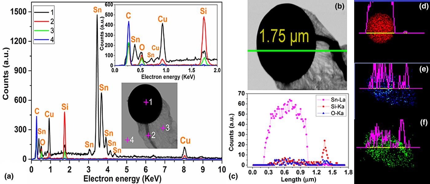
EDS point analysis performed at four different spots for better localized elemental composition is shown in Fig. 5. Spot-4 away from the NW is analyzed for comparison, and this clearly indicates the presence of C and Cu that arise from carbon-coated Cu grid. Spot-2 at catalyst tip shows the presence of a large amount of Sn with little quantity of the Si and O atoms. Multiple peaks of the same element correspond to several possible electron transitions between orbits that emit x-rays with different characteristic energies. Spot-2 at the core of the NW clearly shows a sharp peak for Si that confirms that Si atoms could be the constituent of core NW and more work is to verify with other techniques (STEM EELS) and published later. A weak peak corresponding to O observed in the same spectra appears from the shell of the NW covering the core of a NW. Spot-3 pointed at the shell of the NW depicts its composition having Si and O atoms and their atomic ratio is found to be 48:52 at.%, respectively. Line profile scan [Figs. 5(b) and 5(c)] across the NW indicates the presence of Sn, Si, and O at the tip of the catalyst and a strong peak for Si at the region of the NW indicates that the composition of NW is purely Si. The elemental maps for the respective elements with the line scans are shown in Figs. 5(d)–5(e).
Point and line profile analysis of an individual core–shell nanowire. EDS point analysis at four different positions as shown (inset) in high-resolution STEM image (a) and irrespective EDS spectra from 0 to 10 KeV (a) and 0 to 2 KeV (inset). Line profile scan (b) and spectra (c) across alloy catalyst tip, nanowire, and shell. Elemental mapping for nanowire with catalyst tip as shown in (b) for respective elements; Sn–La (d), O–Ka (e), and Si–Ka (f).

Growth mechanism
NW morphology and growth depends on the material being supersaturated and solidified by precipitation at L–S interface to sustain a continuous growth of a core–shell NW. The nucleation is initiated at the triple phase (solid–liquid–vapor) boundary (TPB), which is generally present at the edge of a catalyst (perimeter encompassing at the edge of a catalyst). Si nuclei is generated at this edge due to the minimization of the nucleation barrier and a newly generated nuclei joins the nuclei at the edge and propagates along the L–S interface to form a layer (a ledge) of Si atoms to form a crystal with more layers piled on the top of each other. The formation of the ledge and the growth of the layers are studied by in situ TEM analysis.[ Reference Hofmann, Sharma, Wirth, Cervantes-Sodi, Ducati, Kasama, Dunin-Borkowski, Drucker, Bennett and Robertson 19 ] However, this study was performed on a single element precipitated NW (i.e., Si). Such a growth process cannot be related to the growth observed here since two different nuclei (Si and SiO x ) should join to form a ledge centered with Si atoms that potentially match with the new layers formed on the top. In recent study, it is proposed that adsorbed Si and O atoms in Sn NP lead to the growth of SiO x NWs from silica seeds accumulated at TPB. Interestingly, this growth process involved a catalyst on the bottom with several silica NWs growing outwards during the cooling process of PECVD where the actual deposition was stopped while the growth precursors are not supplied into the deposition chamber. This growth process is explained with the aid of diffusion-limited aggregation caused by the fractal dendritic pattern.[ Reference Yu, O'Donnell, Alet, Conesa-Boj, Peiro, Arbiol and Roca I Cabarrocas 20 ] However, the growth of SiNW is observed by a standard VLS growth with a catalyst on the top during the growth process and the same catalyst precipitates silica NWs with a catalyst at the bottom during the cooling step of the growth process. Yet, the described growth process is not similar to the growth observed here with a catalyst on the top of the core–shell NWs.
The single step growth of Si–SiO x NWs presented in this work is formed via a self-organization of SiO x clusters terminated with Si atoms bonding with neighboring clusters to establish nuclei of a critical size with Si core, which rapidly spreads out at L–S interface to form a layer. This process is continuously repeated with a continuous feed of Si into a catalyst where the newly formed clusters lead to SiO x clusters with Si core nuclei precipitating at S–L interface to grow NWs. Equilibrium solubility of O in Sn is approximately >45% (±3%) compared with Si at 400 °C.[ Reference Belford and Alcock 21 , Reference Thurmond 22 ] The bond lengths of Si–Si and Si–O are 230 p.m. and 153.3 p.m., respectively, while their bond energy is 226 and 465 kJ/mol, respectively.[ Reference Yu, O'Donnell, Alet, Conesa-Boj, Peiro, Arbiol and Roca I Cabarrocas 20 , Reference Dean 23 , Reference Zhang, Chu, Cheung, Wang and Lee 24 ] Si–O is more stable bond considering the shorter bond length with higher bond energy compared with Si–Si. Hence, the precipitated NW will have more Si–O bonds that form a thick shell of SiO x compared with the Si core. However, with available energy, the formation of both bonds are possible. With the aid of EDX analysis, the atomic ratio of Si to O at catalyst tip is measured as 20:80%. According to the frontier orbital theory, the reactivity of SiO x clusters indicates the formation of Si–Si, O–O, and Si–O bonds where small clusters join to form larger clusters.[ Reference Zhang, Chu, Cheung, Wang and Lee 24 ] The smaller gap of the highest occupied molecular orbitals (HOMOs) and the lowest unoccupied molecular orbitals in SiO x clusters indicate higher chemical reactivity, especially localization of HOMO on the Si atoms at the surface of the cluster leads to a highly reactive region that attracts other clusters to grow. The cohesive energy (energy gained when a surface is created by the formation of the bond from free atoms) per atom in Si-rich clusters at mentioned concentration is very high, signifying less chance of their presence in gaseous phase.[ Reference Zhang, Chu, Cheung, Wang and Lee 24 ] Based on this energetic favorability, the clusters that spread out to form NWs at L–S interface is likely to be in a solid phase.
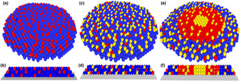
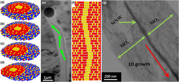
Si sub-oxide clusters are initially formed with incoming Si atoms into a catalyst that is highly reactive and binds with other clusters. SiO x clusters with their high reactivity facilitates the formation of Si–Si bonds with other clusters as discussed earlier. Highly reactive clusters bonding with other clusters form nuclei with Si core which spreads out at L–S interface (Fig. 6). These atoms strongly bind to the substrate and their dangling bonds outward from a surface at the L–S interface attract incoming clusters to spread out to form next layer. A Si–Si bond is formed by merging clusters that lead to the formation of a Si core [Figs. 7(a)–7(d)] and the core size increases with the cluster size. Moreover, Si–Si bonds are formed at the center to reduce the strain energy that also provides the stability of SiO x clusters [Figs. 7(e)–7(f)]. With the formation of SiO x clusters, O atoms diffuse outwards by bond switching due to a high strain observed in large clusters. Theoretically, this was studied by understanding the binding energies of SiO n clusters with the increase of Si core size.[ Reference Zhang 25 ] However, the diffusion length of oxygen atoms outwards from the core depends on strain caused by the size of clusters and the available energy for O atoms in a catalyst, such as the thermal energy (i.e., growth temperature). With the growth of the NWs observed, this work clarifies that SnO catalyst tends to supersaturate, precipitate both Si and SiO x and inert to chemical reactions from other elements present in plasma.
Formation of Si–SiO x nuclei. Cross-sectional sliced top and side view of tin and oxygen catalyst atoms (a, b), with adsorbed silicon atoms (c, d) and Si-core and SiO x shell nuclei that spread by precipitation at vicinity of the L–S interface to grow nanowire (e–f). Spheres in blue, yellow, and red indicate Sn, Si, and O atoms, respectively.

Migration of nuclei that leads to kinked core nanowire that is stable and does not damage/break core nanowire. Cross-sectional sliced top view of Si–SiO x nuclei that spreads by precipitation at the vicinity of the L–S interface and change in nuclei position (a–d) that results in kinked nanowire (e). Change in nuclei position between each layer always binds with Si core of new layer to reduce strain energy that also provides stability of SiO x shell while maintaining the continuous growth of both Si core without any dislocations (f). STEM image of individual nanowire representing 1D growth of core nanowire suppressed with lateral growth (g).

The growth of the core–shell NWs reported here also shows a good control (Supplementary Fig. S3) over NW diameter with 1D growth [Fig. 7(g) and Supplementary Fig. S4]. Such a growth process also inhibits a lateral growth of NWs facilitating controlled vertical growth. Interestingly, the core SiNW within a shell is not broken and accommodates to the stress caused by the kinks. Core SiNWs tend to bend along the direction of the bend observed in the shell without causing damage to the NW.
Conclusion
This work has demonstrated 1D growth of Si–SiO x core–shell NWs to obtain pristine SiNWs at very low temperatures mediated by a metal–oxide alloy catalyst. This work also reveals the use of inorganic and organic tin compounds to obtain tin oxide catalyst alloy that facilitate the growth of NWs. To the best of the author's knowledge, this has demonstrated a novel growth process for the first time. Such a growth process enables the understanding of high-quality SiNWs protected by SiO x shells, from the initial precipitation from the catalyst until its complete growth, which is not influenced by other atomic species present in the plasma. With a SiO x shell, it is possible to achieve 1D growth retarded in the lateral directions. A growth model is proposed to explain simultaneous precipitation of the core and the shell of a NW. The growth process discussed permits the growth of SiNWs coated with other compounds by incorporating chosen atoms in a catalyst. Although it is not performed in this work, if optimized, it might be possible to obtain Si NW covered Si nitride/Si carbide by choosing metal catalysts that have nitrogen and carbon atoms to precipitate a respective compound shell covering the SiNWs. In situ growth of a Si oxide shell across a core SiNW eliminates additional fabrication procedures that might affect the properties of other layers, including NWs in a desired electronic device. With experimental study, we have successfully revealed the growth of a core–shell SiNW and discussed the use of such NWs in electronic devices.
Supplementary material
The supplementary material for this article is available in a separate document which includes characterization techniques, diameter histogram details of core–shell NWs, plot of diameter versus distance along growth axis, and temperature dependance toward growth and morphology of NWs. The supplementary material for this article can be found at https://doi.org/10.1557/mrc.2017.95.