Introduction
Short- and medium-range links, such as in optical communication and data center systems, are dominated by multimode (MM) Vertical-Cavity Surface-Emitting Laser (VCSEL) transmitting data at 850 nm in optical fibers [Reference Mahgerefteh and Thompson1]. In the receiver part of the link, the photodetector is a key element that requires high responsitivity associated with large bandwidth and very low power consumption [Reference Miller2] at the smallest cost. In typical radio-over-fiber receivers, photodetectors are usually followed by transimpedance amplifiers (TIA) to achieve sufficient gain at the cost of complexity and power dissipation. Photodetectors with internal amplification may reduce the constraints on this circuit which would greatly simplify the receiver architecture. At 850 nm, typical photodiodes (PDs) include monolithically integrated avalanche photodiode (APD) [Reference Youn, Lee, Park and Choi3] and PIN PDs [Reference Ciftcioglu, Zhang, Zhang, Marciante, Zuegel and Sobolewski4] in Si. APDs have a large bandwidth and a large responsivity but suffer from a high noise level due to the avalanche process which is subject to quantum and amplification noises and require high operating voltages. Moreover, this solution involves additional process steps compared to industrial Complementary Metal-Oxide-Semiconductor (CMOS) technologies, which leads to increased cost and process complexity. PIN PDs are less costly but suffer from responsivity typically lower than 0.6 A/W at 850 nm because of no internal amplification. An additional candidate would be the Si/SiGe heterojunction bipolar phototransistor (HPT) built-in a Bipolar-Complementary Metal-Oxide-Semiconductor (BiCMOS) technology. The HPT consists of a heterojunction bipolar transistor modified to introduce an optical window, turning it into a photodetector. Under appropriate biasing, the base photocurrent generates an amplified collector current thanks to the transistor effect leading to a high photocurrent gain. Si/SiGe HPTs have been proven to provide high responsivities at low bias and low noise levels [Reference Moutier, Polleux, Rumelhard and Schumacher5–Reference Tegegne, Viana, Polleux, Grzeskowiak and Richalot7].
At a wavelength of 850 nm, high-responsivity has already been demonstrated for phototransistors monolithically integrated with CMOS. In [Reference Shen, Xie, Han, Ge, Yang, Xu, Na, Jin and Zhang8], an HPT with a  $50 \times 50{\unicode{x00B5}}\text{m}^{2}$ optical window using an Analog Foundries process reached a maximal responsivity of 3.198 A/W and a 0.55 GHz bandwidth, while in [Reference Yin, Pappu and Apsel9], an HPT with a
 $6 \times 6{\unicode{x00B5}}\text{m}^{2}$ optical window, built in an 0.25-
 ${\unicode{x00B5}}\text{m}$ BiCMOS process from IBM has a responsivity of 2.7 A/W and a 2-GHz bandwidth. The HPT’s primary problem is their limited bandwidth compared with PIN and APD PDs due to the photogenerated holes current and their higher transit times. Improving the bandwidth of the devices is therefore required to be competitive for high data rate applications. For this purpose, a precise physics-based model could bring a better understanding of the limiting factors for the HPT speed.
This paper presents the implementation for the first time of an Si/SiGe HPT in an industrial technology from STMicroelectronics and the physical model developed with the computer-aided-design software Sentaurus from Silvaco. The HPT design strictly follows the originalBiCMOS process by only proceeding to layout modifications. This leads to a low-cost solution for photodetection. Hydrodynamical simulations are performed to analyze different HPT dimensions with the goal of maximizing their opto-microwave (OM) gain and their frequency response through lateral optical window dimension optimization. The phototransistor operates at the optical wavelength of 850 nm. With the availability of single mode fibers and their reduced spot size, photodetectors with the smallest optical windows are of interest as they lead to better bandwidths and smaller footprints in the chip. Thus, devices with optical window area as small as  $2 \times 2\,{\unicode{x00B5}}\text{m}^{2}$ are studied, and the behavior of photogenerated carriers in the structure is explored, in order to determine the different operating zones inside the HPT layers.
The Si/SiGe phototransistor and its developed physical model
The phototransistor is based on an NPN heterojunction bipolar transistor from STMicroelectronics 55-nm BiCMOS B55X technology [Reference Chevalier, Cacho, Durand, Derrier, Milon and Monsieur11], which is state-of-the-art HBT technology [Reference Gauthier, Brezza, Montagné, Guitard, Azevedo Goncalves and Buczko12]. The intrinsic emitter–base–collector region is stretched and a square optical window is opened above the Si emitter layer and between its metallic contacts. As no additional process steps were made, the fabricated HPTs fully satisfy the foundry design rules. Using Sentaurus software from Silvaco, Si/SiGe HPTs were physically simulated based on their fabrication process while varying the size of the optical window and the geometry of the contacts. The developed physical model is a 2.5D model: the device is designed in 2D and the third dimension is inserted thanks to a multiplication factor on all the currents modeling the device length. The variation of SiGe bandgap energy and absorption coefficient as a function of germanium mole fraction is introduced from [Reference Polleux and Rumelhard14]. A cross-sectional view of the device is shown in Figure 1.
Cross-section of an Si/SiGe BiCMOS phototransistor 2D model developed on Sentaurus with a  $2 \times 2\,{\unicode{x00B5}}\text{m}^{2}$ optical window.

Vertical illumination is generated above the optical window: a Gaussian optical signal varying both in full width at half maximum (FWHM) and optical power can match the typical output of an optical fiber. The distance between the output optical beam and the HPT optical window (airgap) is fit to the corresponding test setup of 15 ${\unicode{x00B5}}\text{m}$ for on-wafer probing characterizations of the HPT. Hydrodynamical simulations of the resulting structures are performed by exploiting drift-diffusion models as previously described in [Reference Moutier, Polleux, Rumelhard and Schumacher5]. Results are described in the section hereafter.
Hydrodynamical simulations
Device simulation for several bias points
The phototransistor is biased with  $V_{\scriptsize{\text{CE}}}=2$ V. It operates in HPT mode when the BE junction is forward biased. Figure 2 shows the simulated static responsivity of a
 $2 \times 2\,{\unicode{x00B5}}\text{m}^{2}$ optical window HPT versus the injected optical power. The static responsivity is calculated as
 \begin{equation}
R_{\scriptsize{\text{OPT}}}(f)=\frac{I_{\scriptsize{\text{HPT}}}-I_{{\scriptsize{\text{DARK}}}}}{P_{\scriptsize{\text{OPT}}}}
\end{equation}
With  $I_{\scriptsize{\text{HPT}}}$ the measured current under illumination,
 $I_{{\scriptsize{\text{DARK}}}}$ the dark current with no illumination, and
 $P_{\scriptsize{\text{OPT}}}$ the injected optical power.
An enhancement of the phototransistor effect is clearly demonstrated in Figure 2. It appears that the responsivity has a peak value when  $P_{\scriptsize{\text{OPT}}}$ reaches levels between 10 and 100 mW. Indeed, the photogenerated holes accumulating in the base generate a local voltage source that decreases the BE potential barrier to enhance the photocurrent gain. Below 10 mW, the value is stable and depends on
 $V_{\scriptsize{\text{BE}}}$ only. Responsivity is optimal for
 $V_{\scriptsize{\text{BE}}}$ between 0.82 and 0.86 V.
Simulated static responsivity of a  $2 \times 2\,{\unicode{x00B5}}\text{m}^{2}$ optical window HPT versus the optical input power at different base bias voltages.

For the following simulations, this last range of voltage will be chosen and the optical power will be in the range of 2 mW to fit previous measurements.
Impact of the optical window size and the emitter contact width
Phototransistors with various optical window widths from 2 to 10  ${\unicode{x00B5}}\text{m}$ were simulated. Because of coupling losses between the fiber and the optical window, FWHM is fixed to be equal to the optical window width. This ensures an equal coupling efficiency for all simulated HPTs. In Figure 3, responsivity at 50 MHz of HPTs with various optical window sizes are presented with varying
 $V_{\scriptsize{\text{BE}}}$ at
 $V_{\scriptsize{\text{CE}}}=2$ V. The optical input is a Gaussian beam of 2.38 mW power.
Responsivity of various HPTs versus the BE voltage.

A maximal responsivity of 1.1 A/W is achieved for the  $2 \times 2\,{\unicode{x00B5}}\text{m}^{2}$ optical window HPT at
 $V_{\scriptsize{\text{BE}}}=0.85\,V$. Indeed, the optical intensity is the highest in the base for this small HPT, which enhances the generation of e–h pairs that contribute to the transistor effect. We observe a saturation of maximal responsivity of 0.8 A/W for optical window widths larger than 4
 ${\unicode{x00B5}}\text{m}$. Larger optical windows bring also larger active emitter area, which increases the dark currents of the device. Thus, the larger HPT may encounter saturation effects that can limit its low-frequency responsivity.
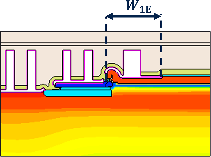
In a bipolar transistor, the collector current strongly depends on the active emitter area, which is located under the emitter contact of the phototransistor (Figure 1). In order to observe the impact of emitter contact area on the active area of the HPT, three different emitter contact widths  $W_{\scriptsize{\text{E}}}$ are tested:
 $W_{\scriptsize{\text{E1}}}=0.48{\unicode{x00B5}}\text{m}$,
 $W_{\scriptsize{\text{E2}}}=0.98{\unicode{x00B5}}\text{m}$, and
 $W_{\scriptsize{\text{E3}}}=1.4{\unicode{x00B5}}\text{m}$. Figure 4 shows the emitter contact when its width is equal to
 $0.48{\unicode{x00B5}}\text{m}$.
Cross section of the HPT: zoom on the emitter contact with a width of  $W_1=0.48{\unicode{x00B5}}\text{m}$.

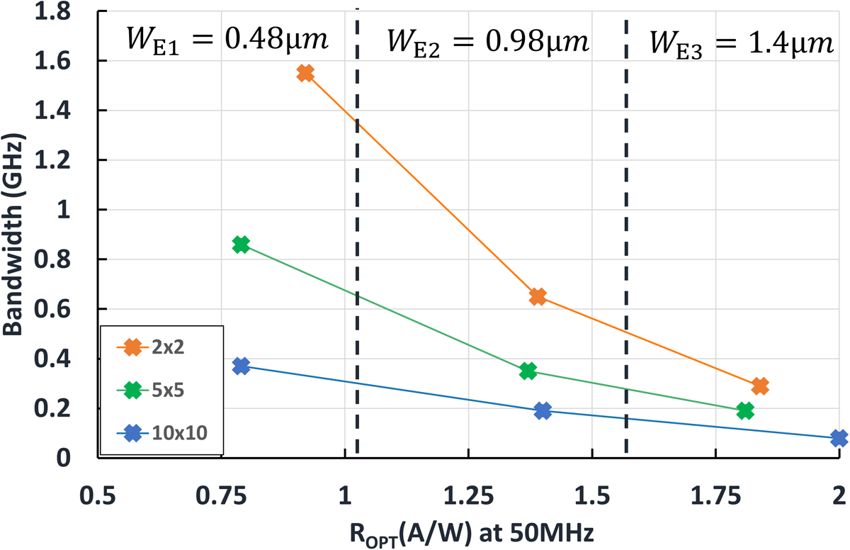
The bandwidth versus the low-frequency responsivity is displayed in Figure 5 for three different optical window widths and three different sizes of emitter contacts.
Simulated bandwidth of various HPTs as a function of their respective low-frequency responsivity under an optical power of 2.38 mW.

The best configuration with the highest responsivity–bandwidth product is for the smallest HPT:  $2 \times 2\,{\unicode{x00B5}}\text{m}^{2}$ optical window HPT with
 $W_{\scriptsize{\text{E1}}}=0.48{\unicode{x00B5}}\text{m}$ (such as in Figure 1). It presents a gain-bandwidth product of
 $R_{{\scriptsize{\text{OPT}}}-\text {LF}}\cdot f_{-3{\scriptsize{\text{D}}}\text{B}}=1.43$ A/W·GHz. A larger active emitter area, introduced by more emitter row contacts, improves the electrical current gain, which leads to higher responsivity, but additional horizontal transit times and increased junction capacitances greatly reduce the bandwidth. For the smallest
 $2 \times 2\,{\unicode{x00B5}}\text{m}^{2}$ optical window size, the bandwidth varies from 1.55 GHz for
 $W_{\scriptsize{\text{E1}}}$ to 0.29 GHz for
 $W_{\scriptsize{\text{E3}}}$. The enlargement of the optical window increases the horizontal photogenerated carrier path which reduces through the device, reducing its bandwidth consequently. The hydrodynamical simulations show that Si/SiGe B55X HPT with a footprint as small as
 $25{\unicode{x00B5}}\text{m}^{2}$ (total footprint of the smallest
 $2 \times 2\,{\unicode{x00B5}}\text{m}^{2}$ optical window HPT) can provide good low-frequency responsivity higher than 0.8 A/W. Table 1 presents the comparison between this work and the state-of-the-art BiCMOS HPT with vertical illumination on responsivity at 50 MHz (
 $R_{\scriptsize{\text{OPT}-50}}{\text{MH}}{\scriptsize{\text{{Z}}}}$), bandwidth (
 $f_{-3{\scriptsize{\text{D}}}\text{B}}$), and their product (GBW for the gain–bandwidth product). Our HPT can exhibit similar responsivity–bandwidth products as the best state-of-the-art Si/SiGe HPT while being integrated into a 55-nm CMOS node which features additional integration capabilities. The B55X HBT is also a state-of-the-art SiGe HBT, which is key to integrate the HPT with best-in-class TIA.
Comparison with state-of-the-art on OM performances

OM gain: different physical contributions
In PD mode of operation, it is possible to isolate the substrate contribution on the OM Gain using the results from [Reference Tegegne, Viana, Polleux, Grzeskowiak and Richalot7] where the substrate current is expressed as:
 \begin{equation}
I_{\scriptsize{\text{SUB}}}=\left(I_{{\scriptsize{\text{C}}}_{\scriptsize{\text{PD}}}}-I_{{\scriptsize{\text{C}}}_{\scriptsize{\text{PD}}}}-{\scriptsize{\text{DARK}}} \right)-\left(I_{{\scriptsize{\text{B}}}_{\scriptsize{\text{PD}}}}-I_{{\scriptsize{\text{B}}}_{\scriptsize{\text{PD}}}-{\scriptsize{\text{DARK}}}} \right)
\end{equation}
With  $I_{{\scriptsize{\text{C}}}_{\scriptsize{\text{PD}}}}$,
 $I_{{\scriptsize{\text{B}}}_{\scriptsize{\text{PD}}}}$, the collector and base currents in PD bias under illumination and
 $I_{{\scriptsize{\text{C}}}_{\scriptsize{\text{PD}}}}-{\scriptsize{\text{DARK}}}$,
 $I_{{\scriptsize{\text{B}}}_{\scriptsize{\text{PD}}}}-{\scriptsize{\text{DARK}}}$, the collector and base current in PD mode biasing with no illumination. As the substrate current is independent of the base bias voltage, we can extract the substrate responsivity of the HPT from:
 \begin{equation}
R_{\scriptsize{\text{SUB}}}(f)=R_{\scriptsize{\text{OPT}}}(f)-X_{\scriptsize{\text{OPT}}}(f)
\end{equation}
With  $R_{\scriptsize{\text{OPT}}}$, the responsivity gathered at the collector contact and
 $X_{\scriptsize{\text{OPT}}}$, the responsivity gathered at the base contact.
The contribution of the intrinsic region of the phototransistor (emitter + base + collector) can then be computed:
 \begin{equation}
R_{{\scriptsize{\text{OPT}}}_{\text{I}{\scriptsize{\text{NTR}}}}}(f)=R_{\scriptsize{\text{OPT}}}(f)-R_{\scriptsize{\text{SUB}}}(f)
\end{equation}
Introducing Eq. (5) with Eq. (3) and Eq. (4), the respective contribution of the substrate and the intrinsic part of the HPT can be extracted.
Figure 6 presents the hydrodynamical simulation of the OM gain for a  $2 \times 2\,{\unicode{x00B5}}\text{m}^{2}$ optical window HPT with 1 emitter contact row (such as the one represented in Figure 1). Both the PD mode (
 $V_{\scriptsize{\text{BE}}}=0$ V) and the phototransistor mode (
 $V_{\scriptsize{\text{BE}}}=0.82$ V) are represented.
OM gain of a  $2 \times 2\,{\unicode{x00B5}}\text{m}^{2}$ optical window HPT with its different contributions.

In PD mode, the intrinsic contribution to the OM gain is negligible compared to the substrate contribution ( $G_{{\scriptsize{\text{OM}}}_{\scriptsize{\text{SUB}}}}=-24$ dB and
 $G_{{\scriptsize{\text{OM}}}_{{\scriptsize{\text{PD}}}-\text{I}{\scriptsize{\text{NTR}}}}}=-46$ dB). Indeed, most of the photogenerated carriers contributing to the collector output current in this mode are generated inside the substrate–collector junction or deeper in the collector layer.
In HPT mode, the intrinsic contribution dominates over the substrate one ( $G_{{\scriptsize{\text{OM}}}_{\scriptsize{\text{SUB}}}}=-24$ dB and
 $G_{{\scriptsize{\text{OM}}}_{{\scriptsize{\text{{HPT}}}}}}-\text{I}{\scriptsize{\text{NTR}}}=-1.8$ dB). This is due to the photogenerated holes in the base that contribute to the transistor effect enhancing the electrical current gain. The bandwidth of the intrinsic part of the device in HPT mode is equal to 1.52 GHz which is slightly higher than the substrate bandwidth which is about 1.3 GHz. The overall bandwidth of the HPT is 1.43 GHz. The substrate contribution to the overall OM gain is negligible on the frequency response. The device bandwidth is mainly reduced by the horizontal transit times of the photogenerated holes below the optical window diffusing to the base contact with a slow transit velocity [Reference Shen, Xie, Han, Ge, Yang, Xu, Na, Jin and Zhang8] and by the large BC junction capacitance.
Photogenerated carrier behavior in the HPT
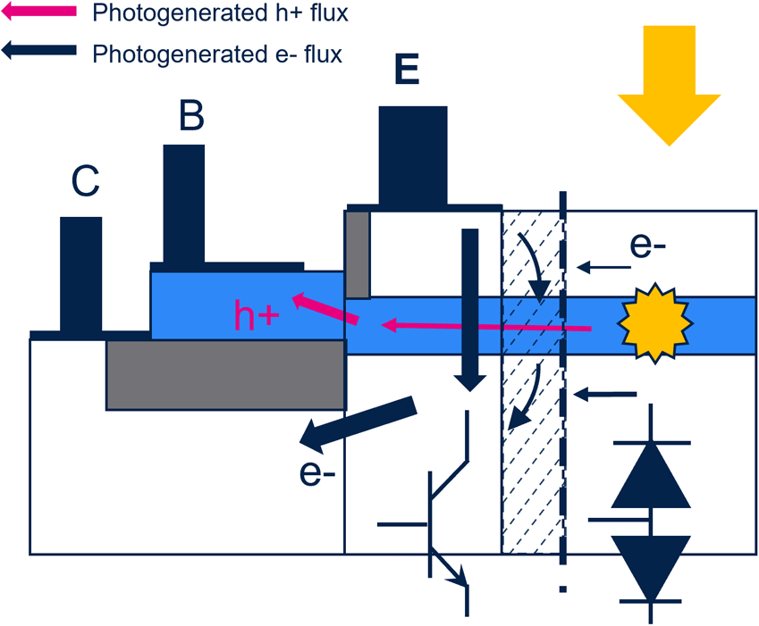
The extension of the emitter active region below the optical window leads to an increase of the junction capacitances, thus, degrading the bandwidth of the device. A schematic of this particular expansion is proposed in Figure 7.
Schematic of the left side of an HPT with the photogenerated carrier flux.

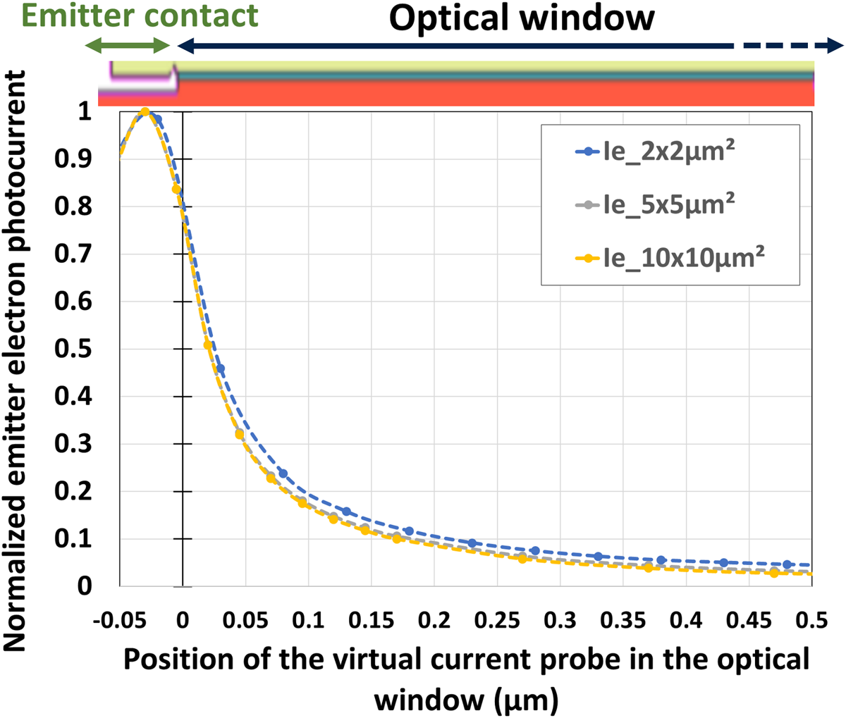
A virtual current probe is used by simulations to evaluate the local electron and hole currents at different points of the structure. As identifying the expansion of the active emitter area is desired, only the current due to the phototransistor effect is of interest. This current is the emitter electron current generated to compensate holes that cross the BE junction (Figure 7). Figure 8 plots this specific current for three different optical window sizes. Only the vertical contribution of this photocurrent is related to the photocurrent amplification effect.
Simulated normalized emitter electron photocurrent versus the virtual current probe position on the optical window for 3 HPTs,  $P_{\scriptsize{\text{OPT}}}=2.38$ mW.

Figure 8 shows that the extension of the active emitter is not dependent upon the optical window width. The size of the optical window plays a minor role in this extension. The phototransistor structure can be delimited into two areas:
(1) One absorption area below the optical window: electron–hole pairs are generated in the pn junctions.
(2) One amplification area where the transistor effect occurs. This area is delimited by the active emitter region of the device which is located under the emitter contact but with an additional extension in the optical window.
Comparison between measurements and simulation results
In this last section, hydrodynamical simulations from the physical model are compared with results from measurements in order to validate the model.
Gummel plots
Gummel plots are obtained by measuring base and collector currents while sweeping the collector–emitter voltage  $V_{\scriptsize{\text{CE}}}$. On-wafer measurements were realized using Ground-Signal-Ground (GSG) probes. Biasing of the base and collector ports was performed by a Keysight B1500 Semiconductor Device Analyzer. A V25-850M VCSEL from VI Systems with an 850-nm emission wavelength was used as the optical source, it was biased by a Keysight 6625A precision system power supply. A multimode optical fiber (MMF) of
 $50{\unicode{x00B5}}\text{m}$ core at the output VCSEL is aligned with the top of the HPT optical window using nanopositioners. A
 $22\,{\unicode{x00B5}}\text{m}$-FWHM was measured at a
 $15{\unicode{x00B5}}\text{m}$-airgap between the optical window and the optical fiber tip. The HPT with a
 $10 \times 10{\unicode{x00B5}}\text{m}^{2}$ size was characterized under an optical power of 2.177 mW at the output of the optical fiber.
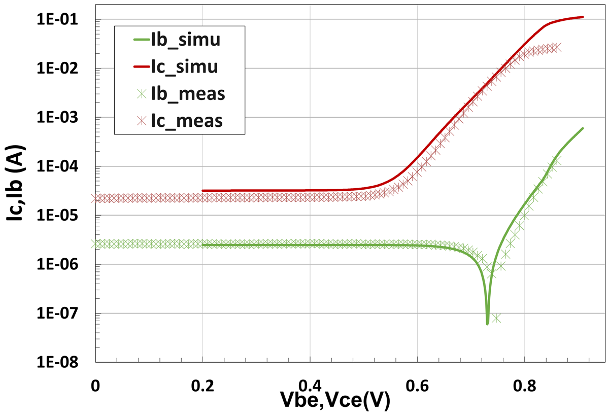
Results of Gummel curves under illumination for both simulation and measurements are presented in Figure 9.
Comparison between simulation and measurements: Gummel plots of a  $10 \times 10{\unicode{x00B5}}\text{m}^{2}$ optical window HPT under
 $P_{\scriptsize{\text{OPT}}}=2.177$ mW at 850-nm wavelength.

At low  $V_{\scriptsize{\text{BE}}}$ and
 $V_{\scriptsize{\text{CE}}}$, lower than 0.7V, the current levels are constant as photocurrents generated in the BC junction are dominant, and the device works in PD mode. Simulation fits the measured current curves quite well. The simulated collector current is slightly higher than the measured one:
 $32\,{\unicode{x00B5}}\text{A}$ versus
 $23{\unicode{x00B5}}\text{A}$. This is due to the presence of metallic transmission lines around the optical window. Under measurements, these transmission lines absorb a part of the optical injected power, while it is absorbed in the substrate in simulations, thus, generating e–h pairs in the substrate–collector junction that increases the collector current consequently. When
 $V_{\scriptsize{\text{BE}}} \gt 0.6$ V, the transistor effect starts and the device works in HPT mode. Simulated currents fit well with measured currents in such mode as well with some restrictions in the high injection regime.
OM gain
The OM gain [Reference Viana, Tegegne, Polleux and Algani13] is measured using a 40-GHz Vector Network Analyzer (VNA) 8722ES from Keysight. A K-cable connects the VNA port1 to the electrical input of the 18-GHz bandwidth VCSEL modulated the optical carrier by an RF signal of −15 dBm. The optical signal is transmitted by a lensed multimode fiber ( $\text{FWHM} = 16.5{\unicode{x00B5}}\text{m}$) to the phototransistor optical window. On-wafer GSG probe is aligned on the HPT collector to the VNA port2 via K-cable. The HPT base and collector are biased by the Keysight B1500 Semiconductor Device Analyzer through bias tees. The
 $S_{{21}}$ scattering parameter computes the OM gain of the device under 50 Ω. Measurements post-processing of the raw data are performed to remove contributions of both the optical link, GSG probe, and K-cable on the
 $S_{{21}}$ parameter.
The OM gain can be computed on Sentaurus through an optical AC analysis and the quantum efficiency simulation as a function of the frequency [15]. A small variation on the incident optical signal is obtained varying the photogeneration rate in the structure and changing the quantum efficiency for each contact. From these parameters, we can obtain the responsivity of the collector contact and the base contact. The OM gain on a 50-Ω load is then computed:
 \begin{equation}
G_{{\scriptsize{\text{OM}}}}=\frac{1/2\cdot R_{0}\cdot I_{\scriptsize{\text{C}}}-50{\Omega}^{2}}{1/2\cdot R_{0}\cdot P_{\scriptsize{\text{OPT}}}^2}\cdot \frac{1}{\alpha^2}=\left\lvert\frac{R_{{\scriptsize{\text{OPT}}}-50\Omega}}{\alpha}\right\rvert^2
\end{equation}
with α = 1 A/W an homogenization coefficient and  $ R_{{\scriptsize{\text{OPT}}}-50\Omega}$, the dynamic responsivity at the collector contact when the base and the collector are loaded to 50 Ω.
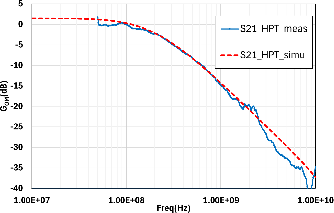
Comparisons between measurements and simulations of a  $10 \times 10{\unicode{x00B5}}\text{m}^{2}$ optical window HPT are presented in Figure 10. The HPT is voltage biased with
 $V_{\scriptsize{\text{BE}}}=0.82$ V,
 $V_{\scriptsize{\text{CE}}}=2$ V. It is illuminated with an optical power of 1.45 mW at the output of the lensed optical fiber.
Comparison between simulation (red) and measurements (blue): OM gain of the HPT for  $V_{\scriptsize{\text{CE}}}=2$V,
 $V_{\scriptsize{\text{BE}}}=0.82$V under
 $P_{\scriptsize{\text{OPT}}}=1.45$ mW at 850 nm.

At low frequency, the OM gain at 50 MHz is 1.5 dB for simulation and 0.3 dB for measurements. The bandwidth difference is less than 30 MHz,  $f_{-3{\scriptsize{\text{D}}}\text{B}}=187$ MHz for the simulation and
 $f_{-3{\scriptsize{\text{D}}}\text{B}}=220$ MHz for the measurement. The good match between simulation and measurement for multiple bias points allows us to validate the physical model and confirm its use to predict the performances of HPTs.
Conclusion
An Si/SiGe HPT has been implemented for the first time into a 55-nm BiCMOS STMicroelectronics technology. No changes in the process were made: the HPT devices can be easily integrated on-wafer with CMOS transistors and can easily be available for the production. The integration of HPT in such a mature platform leads to further microwave photonic circuit development above the cutoff frequency through a direct HPT+HBT combination. It also allows low-cost phototransistors and supports the convergence between photonics and microwaves. This paper demonstrates an excellent fit between simulation and measurements through a well-chosen set of physical parameters of the hydrodynamic simulation. One of the most important parameters is the exploitation of the real topology of the HPT and an efficient optical absorption coefficient model. Based on this trustable model, it can be inferred that the optimization of SiGe HPT needs a specific care in the emitter width and optical window size. Further optimization should be permitted in the future with this model. The behavior of the HPT has been studied to better understand the photocurrent amplification and an analysis on the optimal layout has been performed. Simulations show that phototransistors with a  $2 \times 2\,{\unicode{x00B5}}\text{m}^{2}$ optical window and minimal emitter contact area can be optimized to a responsivity–bandwidth product of 1.43 A/W·GHz for a 1.6-GHz bandwidth with a very small footprint.
Such phototransistors are a viable solution for low-cost optical interconnects in silicon CMOS and improving the coupling efficiency between those small HPTs and the optical fiber could further increase the performance of these low-cost, high-integration and high-responsivity photodetectors.
Acknowledgements
We would like to thank people from STMicroelectronics involved in the development and fabrication of B55X wafers, including the design of the HPT cells and their physical modeling.
Competing interests
The authors declare none.

Valentin Thary received his master’s degree in electronic engineering from the Grenoble-Alpes University in 2021. In 2022, he started his PhD at the Gustave Eiffel University (France) on low-cost Si/SiGe Phototransistors for microwave photonic communication applications. His work is focused on the development, characterization, and modeling of Si/SiGe phototransistors.

Catherine Algani received, from the University of Paris 6, France, the DEA and PhD degrees in Electronics, respectively, in 1987 and 1990. Her dissertation concerns the area of active MMIC design using GaAs HBTs technology in CNET-Bagneux. In 1991, she joined the electronics engineering department and the LISIF Laboratory, at the University of Paris 6, as a lecturer. From 1991 to 2005, she worked on the design of microwave and millimeter-wave-integrated circuits on different GaAs technologies. In 1997, she began to work in the area of microwave photonics (optically controlled microwave switches on GaAs and electro-optic organic modulators). In 2005, she joined ESYCOM at CNAM-Paris, where she is currently a full professor. Her current research interests are the development of devices, circuits, and sub-systems for ultrahigh-speed digital and analog communications for ROF and wireless applications. This research includes the modeling, the design, and the characterization of such structures.

Jean-Luc Polleux (Member, EuMA) is CTO and cofounder of the start-up ICON Photonics, in Paris region, France. He received the PhD degree in the opto-microwave field from CNAM, Paris, in 2001. He joined in 2001 ESIEE Paris-Université Gustave Eiffel and ESYCOM-CNRS laboratory as an associate professor and researcher, respectively. He was Director of International Relations of ESIEE Paris from 2016 to 2022 and he cofounded the ICON Photonics startup in 2018. His research involved microwave and photonic devices and systems for radio-over-fiber applications and Free-Space-Optics. Dr J.L. Polleux is the initiator of the world’s first SiGe/Si microwave phototransistors. He has pushed further the technology through device modeling, characterization, and their circuit integration since then. Since 2022, he has been full-time CTO of ICON Photonics where he develops on-wafer-level optical and electrical interconnects for high-speed optical communications and quantum applications. Dr Polleux has authored or co-authored over 100 technical journal papers and conference publications.

Pascal Chevalier Pascal Chevalier (Member, IEEE) received the PhD degree in electronics from the University of Lille, France, in 1998, for his work on InP-based HEMT. He joined Alcatel Microelectronics, Belgium, in 1999, where he contributed to the start of RF BiCMOS. Since joining STMicroelectronics, Crolles, France, in 2002, he has been working on the development of SiGe BiCMOS and RF-SOI CMOS technologies and related devices, with a long-lasting research interest in SiGe HBT. He led the RF-SOI CMOS, BiCMOS & Photonics Technologies R&D team. He is currently an Analog/RF Technology Architect and is a Fellow of Technical Staff. Dr Chevalier has authored or co-authored over 200 technical journal papers and conference publications. He has served on the Technical Program Committees of the IEEE BCTM, the ECS SiGe Symposium, the IEEE BCICTS, and the IEEE IEDM conferences. He has been a member of the RF & AMS Technologies section of the ITRS of which he led the Silicon Bipolar & BiCMOS subgroup.