I. INTRODUCTION
A thin hetero-epitaxial film deposited on a dissimilar substrate will inevitably result in residual stressesReference Freund and Suresh1–Reference Anzalonea, Camarda, Locke, Carballo, Piluso, La Magna, Volinsky, Saddowb and La Viab3 and microstructural defects such as micro-twinsReference Maurice, Durand, Drouet and Contour4–Reference Liu, Zhang and Zhang6 and dislocationsReference Maree, Barbour, Vanderveen, Kavanagh, Bullelieuwma and Viegers7–Reference Ning, Chien, Pirouz, Yang and Khan10 due to the mismatches of lattice structure and thermal expansion. These defects can significantly degrade the electronic properties of the device.Reference Iborra, Olivares, Clement, Vergara, Sanz-Hervás and Sangrador11–Reference Smith13 To improve the product quality and minimize the defects, an epitaxial re-growth is often exploited,Reference Lau, Matteson, Mayer, Revesz, Gyulai, Roth, Sigmon and Cass14,Reference Paine, Howard, Stoffel and Horton15 which involves ion implantation to induce point defects and amorphous structure and annealing to achieve a solid phase epitaxial (SPE) re-growth.
A typical hetero-epitaxial thin film system of silicon-on-sapphire (SOS) has a high lattice mismatch strain of 5.9% in Si [100] and 14.1% in Si [010] directions. The deposition and cooling produce significant compressive stresses of 700–800 MPa,Reference Liu, Zhang, Brawley, Atanackovic and Duvall16 which are much smaller than those expected from the misfit strains. This is the result of domain mismatch epitaxy (DME),Reference Narayan and Larson17,Reference Bayati, Molaei, Narayan, Narayan, Zhou and Pennycook18 bringing about the high-density misfit dislocations at the interfaceReference Abrahams, Buiocchi, Corboy and Cullen19,Reference Liu, Ruan, Zhang and Moridi20 to minimize the effect of the significant lattice mismatch strains. The silicon film also contains high density of threading dislocations and stacking faults,Reference Cristoloveanu21,Reference Anidow22 resulted from the three-dimensional island growth process.Reference Hamarthibault and Trilhe23 To further improve the crystalline quality, implantation and annealing processes have been used.Reference McKenzie, Domyo, Ho and Munroe24–Reference Amano and Carey26 It has been demonstrated that high temperature annealing on the implanted specimens can reduce residual stresses,Reference Ohmura, Inoue and Yoshi27–Reference Dubbelday, Kavanagh and Fitzgerald29 even though the mismatches of thermal expansions and lattice constants remain unchanged. For example, Ohmura et al.Reference Ohmura, Inoue and Yoshi27 investigated the residual stresses in the silicon film of an SOS system using a 2-step annealing, first at 600 °C and then at a range from 600 to 900 °C. They found that the annealing temperature at the second step vanishingly affected the stress reduction and therefore speculated that the stress reduction was caused by a new interface formed in the first 600 °C annealing, which can sustain up to 900 °C in the second annealing. Beyond this threshold temperature, the new interface would be destroyed, leading to a regeneration of residual stresses to the as-grown level. Bolotov et al.Reference Bolotov, Efremov, Karavaev, Volodin and Golomedov28 correlated the stresses and microstructures with doping conditions and suggested that the stress relaxation was induced by the formation of vacancies at the film-substrate interface. If a sample was annealed at a sufficiently high temperature, the vacancies would reduce and the residual stresses would increase. Dubbelday and KavanaghReference Dubbelday, Kavanagh and Fitzgerald29 measured the strains in the silicon film annealed at 700 to 1000 °C for different durations. They found that the in-plane strains oscillated for an annealing of only 5–7 min and then approached the theoretical thermal mismatch strains. They ascribed this kind of early strain oscillation to the annealing-induced diffusions of implanted Si+ from sapphire to silicon, which induces a tensile strain at the early stage of the annealing. Other studies conceived that the relief of residual stresses was associated with the increased density of misfit dislocationsReference Misra and Swain30 and dislocation loopsReference Mantl, Holländer, Liedtke, Mesters, Herzog, Kibbel and Hackbarth31,Reference Trinkaus, Holländer, Mantl, Herzog, Kuchenbecker and Hackbarth32 induced by implantation and annealing. Due to these investigations, implantation and annealing have become a standard process in producing SOS. However, it is still counterintuitive that a better crystal quality can be associated with less stress since the former brings about more stringent mismatch between the film and the substrate. This apparent dilemma, remaining unresolved in the literature, makes the selection of dose density, implantation energy and annealing temperature in a rather floppy way, leading to many failures in production.
The aim of this paper is to reveal, from the grass roots, the effects of the implantation and annealing and the mechanisms of residual stress relief and microstructural change. The SOS samples obtained from CVD deposition were used. They were doped with Si+ implants with different energies and densities. The implanted samples were then annealed at various temperatures. Raman scattering and TEM techniques were used to assist to explore the effects of implantation and heat treatment.
II. EXPERIMENT
The samples were (001) silicon films of thickness 280 nm, deposited on a  $(10\bar 12)$ sapphire substrate of thickness 600 μm at 900 °C by chemical vapor deposition (CVD). The in-plane alignments are Si [100]||Al2O3
 $[\bar 1101]$ and Si [010]||Al2O3
 $[11\bar 20]$. The as-deposited SOS samples were subjected to a Si+ implantation at room temperature under two implanting energy levels, 135 and 200 KeV, and three dose densities, 1014, 1015, and 5 × 10¹⁵ ions/cm2. To avoid any self-annealing during implantation, the temperature of the samples were kept at 25 °C by active cooling with liquid nitrogen. The implanted samples were then annealed in a furnace for 1 h at 600, 700, 800, 900, and 1000 °C, respectively, and cooled down inside the furnace for half an hour before the final cooling in air.
The residual stresses of the implanted and annealed samples were measured at room temperature by Raman Scattering with a Renishaw Invia unit equipped with backscattering configuration. A standard setup of 514 nm Argon ion laser and 1800 L/mm grating was utilized to detect the silicon band at around 520.5 cm−1. The incident light was focused on the (001) surface of the silicon film using a 20x microscope objective. The scattered light was collected by the same objective. The spot size of the incident beam was about 2 μm and the penetration depth in Silicon was about 0.77 μm.Reference DeWolf33 Using this setup, a spectral resolution of 1.7 cm−1 was obtained. The residual stress in the epitaxial silicon film was assumed to remain equi-biaxialReference Liu, Zhang, Brawley, Atanackovic and Duvall16 and could be measured by the shift of the Raman band Δω (cm−1). To find the peak position of the crystalline silicon (c-Si) band, the Raman spectra were fitted with Gaussians. The minima of the second derivative of the fitted function were then searched at around 520.5 cm−1. In doing so, the in-plane normal stress σ could be uniquely related to the frequency shift Δω by σ = −249Δω (MPa).Reference Englert, Abstreiter and Pontcharra34 It has been shown that the residual stress calculated by this equation is consistent with the XRD stress measurement.Reference Liu, Zhang, Brawley, Atanackovic and Duvall16
The microstructures of the re-growth SOS samples were studied using the transmission electron microscopy (TEM), using the cross-sectional specimens along silicon [110] prepared by a Nova 200 Nanolab (FEI, Hillsboro, OR) focused ion beam (FIB) system. In the FIB milling process, the silicon film was protected by Pt deposition on the surface. The TEM specimens were milled by Ga ion beam at 30 KV and 0.63 nA. The AutoTEM software was used to reduce the thickness to less than 100 nm for a better lattice view. The TEM specimen was tilted around the silicon <110> zone axis by a double tilt holder in a Philips CM-200 TEM (Philips, Hillsboro, OR) to obtain the bright-field images and the high resolution lattice images under a 200 KeV electron beam.
III. EXPERIMENTAL RESULTS
A. Effect of implantation
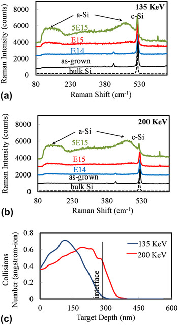
The ion implantation can modify microstructure of the as-grown film by introducing the vacancies and interstitial defects (Frenkel pairs). The accumulation of these defects results in the dislocation loops. When the deformation energy reaches a critical value of 12 eV/atom, the crystalline-to-amorphous phase transformation occurs.Reference Narayan35,Reference Gibbons36 The depth and thickness of the amorphous phase depend on the dose density and implantation energy. In the Raman spectra of the implanted specimens, as shown in Figs. 1(a) and 1(b), the occurrence of the broadened peak at a small wave number indicates the phase transformation from c-Si to amorphous silicon (a-Si). The results showed that under both the energy levels, the amorphous fraction increases with increasing the Si+ doses. Narayan and HollandReference Narayan35 have shown that the amorphous phase nucleates at the region of the maximum number of collisions and then expands toward the surface and the deeper region with the increase of implanted ion doses. With the same dose density, a higher energy (e.g., 200 KeV) resulted in a larger amorphous fraction. This is because an implanting ion, which carried more energy can penetrate deeper, collide with more lattice atoms, and have a longer mean-free path than the lower energy condition. The nominal distributions of collision events were simulated by the software TRIM (Transport of Ions in Matter), as shown in Fig. 1(c) for energy levels of 135 and 200 KeV. It reveals that under the extreme conditions in the present study, i.e., 200 KeV and 5 × 10¹⁵ ions/cm2, the ion implantation induced damage should have significantly changed the silicon/sapphire interface. Moreover, in both of the conditions, the least collisions occur in the layers close to the surface, where the crystalline structure should be preserved. This provides seeds for the film re-grown in annealing.Reference Lau, Matteson, Mayer, Revesz, Gyulai, Roth, Sigmon and Cass14
Raman spectra on the as-implanted samples subjected to the energies of (a) 135 KeV and (b) 200 KeV; (c) TRIM simulation of collision events. The curves E14, E15, and 5E15, respectively stand for Si+ dose densities of 1014, 1015 and 5 × 10¹⁵ ions/cm2.

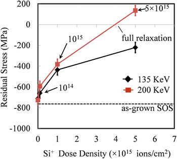
The variations of residual stresses in the specimens implanted with different energies and dose densities are summarized in Fig. 2. Clearly, the implantation brought about a significant reduction of residual stresses in the silicon film. The increase of both the ion density and implantation energy resulted in more stress relief. This is because the heavier doping conditions give rise to more vacancies, dislocations and amorphous transformations, so as to alleviate more elastic strain (compressive) in the lattice. However, it is surprising to note that the residual stress became tensile under the extreme condition—dose density of 5 × 10¹⁵ ions/cm2 and implantation energy of 200 KeV. This is unexpected because the effect of amorphization should only alleviate the existing stress rather than induce a stress of opposite direction. This will be further discussed in Sec. IV.
Room temperature residual stresses measured on the as-implanted samples.

B. Effect of annealing
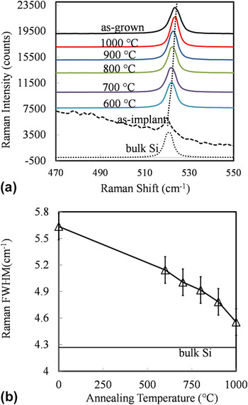
Annealing after implantation is to restore the crystalline structure through epitaxy re-growth. Fig. 3 shows the Raman spectrum of the annealed samples (implantation conditions 200 KeV and 5 × 10¹⁵). The annealing at 600 °C has smeared out most of the amorphous phase, leaving only a sharp peak at about 521 cm−1. This indicates the domination of the c-Si after annealing. It is also noted that increasing the annealing temperatures brought about a better crystalline quality of the Si film, evidenced by the decrease of the FWHM (full width half maximum) of the c-Si Raman band as shown in Fig. 3(b). A possible explanation for such crystalline quality improvement is that the higher temperature has resulted in a higher mobility of dislocations, thereby brought about their higher rate of annihilation.Reference Aindow, Batstone, Pfeiffer, Phillips and Pond25
(a) Raman spectrum of the implanted samples annealed at different temperatures, and (b) Variations of Raman FWHM with annealing temperatures. The samples were implanted with Si + at 200 KeV and 5 × 10¹⁵ ions/cm2.

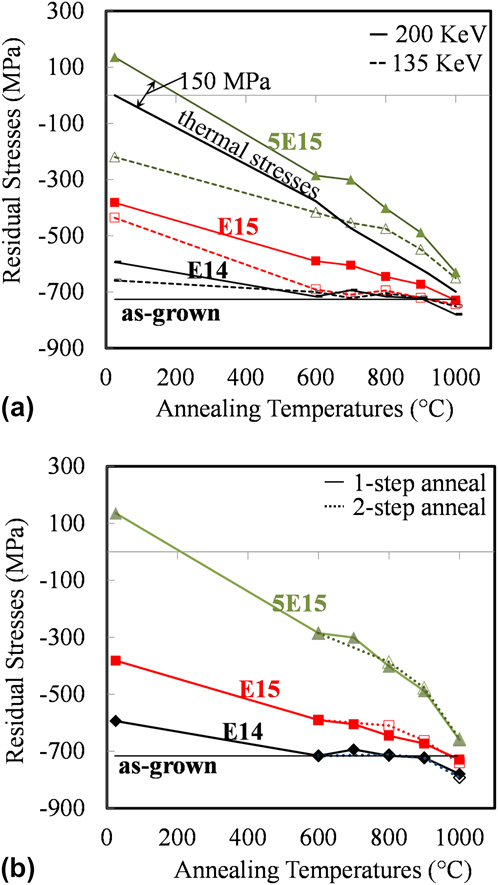
The apparent right shifts of Raman peaks with increased annealing temperatures, as demonstrated in Fig. 3(a), indicate the restore of compressive residual stresses in the silicon film. To better understand the effect, the variation of residual stresses versus annealing temperature is given in Fig. 4(a), where the continuous and dashed lines pertain to samples subjected to 200 and 135 KeV implantations, respectively. The result shows that a higher annealing temperature renders greater residual stress regeneration. For the samples implanted with smaller dose densities, the annealing at the deposition temperature (900 °C) can regenerate the residual stresses to the as-grown level. It is noted that the lighter the doping (i.e., smaller implantation energy or less dose density), the lower annealing temperature is needed to restore the residual stresses to the as-grown level.
Stress variations with annealing temperatures. The comparisons are to illustrate the effects of (a) implanting energies and (b) annealing method on residual stresses. Si+ dose densities are 1014, 1015 and 5 × 10¹⁵ ions/cm2 for the curves E14, E15, 5E15, respectively.
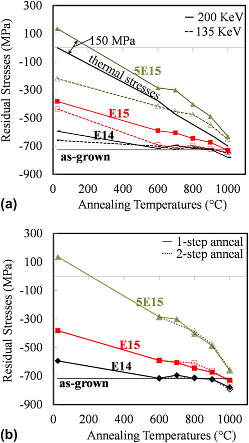
The highest rate of residual stress regeneration was observed in the sample subjected to the heaviest implantation. As indicated by the solid black curve in Fig. 4(a), this rate is consistent with the variation rate of residual stresses obtained by taking into account only the mismatch of coefficients of thermal expansion (CTE).Reference Moridi, Ruan, Zhang, Liu and Haddad37 However, the whole stress-temperature curve shifts upwards with a rather constant offset of about 150 MPa. This indicates that heating to and annealing at different temperatures cannot remove the tensile stresses induced by implantation. If the tensile stress is due to the amorphization of the Si layer, it should be effectively removed after the annealing and crystal re-growth. This, however, did not take place. Therefore, the implantation-induced tensile stress must have its structural origin at the interface.
To further confirm the above findings, let us examine a 2-step annealing method,Reference Ohmura, Inoue and Yoshi27 with which an implanted sample was first annealed at 600 °C for an hour and then further annealed at temperatures ranging from 700 to 1000 °C. Figure 4(b) shows the stresses measured at room temperature after the 2-step annealing. For all the implanted samples studied, it was found that the variation of the stresses with the highest annealing temperature is consistent with that obtained from the single step annealing shown in Fig. 4(a). It is therefore reasonable to conclude that the final residual stresses are only dependent on the highest annealing temperature and are not affected by the 1st annealing at 600 °C.
IV. STRESS RELEASE MECHANISM
The above experimental results demonstrate that different implantation and annealing conditions indeed brought about different residual stresses. As such, the following questions need to be answered:
(i) Why do different ion densities and implantation energy levels render different residual stress relief?
(ii) Why do samples subjected to different implantation conditions exhibit dissimilar stress variations during their subsequent annealing?
(iii) What causes the tensile stress in the sample that was most heavily implanted?
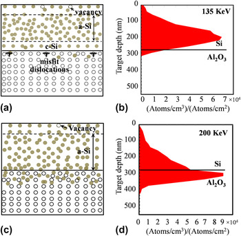
It has been shown that with the increase of ion doses, the accumulation of vacancies and interstitial point-defects brings about dislocation loops and amorphous clusters, which results in more stress mitigation. With the same dose density, a higher energy further enhances the stress relief by two mechanisms, as illustrated in Fig. 5. Firstly, compared to the lower energy condition [Fig. 5(a)], the high-energy [Fig. 5(c)] implantation shifts the maximum number of the collisions toward the interface, leading to more amorphous phase in the vicinity of the interface. With a greater interface amorphization, the lattice mismatch stress could be more effectively alleviated. Secondly, as shown from the TRIM simulation of the ion ranges [Figs. 5(b) and 5(d)], silicon ions with a larger energy can penetrate into the substrate, resulting in substitutional point-defects in the sapphire substrate. These excessive ions eventually expand the sapphire lattice, and lead to the tension in the film. It can be expected that at a certain density of the ion dose, e.g., at about 4 × 10¹⁵ shown in Fig. 3, the two effects will bring about a full relaxation of the compressive residual stress and even the tensile stress in the film.
Schematics of implantation energy effects on the microstructures (a) and (c), and the ion resting ranges (b) and (d) simulated by TRIM software; the implantation energy was 135 KeV for (a) and (b) and 200 KeV for (c) and (d).

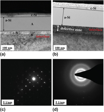
The effects of implantation of different energy levels were exhibited by the TEM images as shown in Fig. 6. For the low-energy implantation [Fig. 6(a)], owing to the limited penetration depth of the ions, the crystalline interface between film and substrate is still preserved, which is proven by the diffraction pattern [Fig. 6(c)] taken from the interface region “B” of Fig. 6(a). In Fig. 6(c), the overlapped diffraction patterns of the single crystalline silicon and sapphire are well discerned. Inside the silicon film, the high dose density of 5 × 10¹⁵ ions/cm−2 has fully transformed c-Si to a-Si, as indicated by the diffraction pattern [Fig. 6(d)] taken from the region “A” of Fig. 6(a). In contrast, the higher-energy implantation [Fig. 6(b)] has completely transformed the interface to be amorphous and produced a defective zone in sapphire adjacent to the interface, whereas this defective zone was not observed under the low-energy condition.
TEM bright field images of as-implanted SOS subjected to the doping energies of (a) 135 KeV and (b) 200 KeV; (c) and (d) are respectively the diffraction patterns taken at the interface “B” and amorphous area “A” in (a). The ion dose density for both of the specimens was 5 × 10¹⁵ ion/cm2. The samples were tilted to the sapphire <0112> zone axis.

Different implantation conditions give rise to different interface structures. For the lightly doped samples that preserve the as-grown interface structures, the primary effect of annealing was to recover the implantation defects (e.g., vacancies and dislocation loops). In this case, an annealing temperature as high as 900 °C was sufficient to smear out most of those defects, and restored the residual stress to the as-grown level. However, the heavy implantation could substantially modify the interface structure. As shown previously in Fig. 4(a), the high temperature annealing restored the crystalline structure and the subsequent cooling led to the thermal stress induced by the CTE mismatch. However, the constant offset of about 150 MPa from the reference curve seems to imply that the expansion in the substrate could not be removed by annealing.
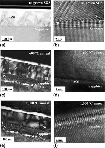
The microstructural variations from the as-grown and re-grown SOS are illustrated in Fig. 7. Compared with the as-grown film [Fig. 7(a)], the TEM images of samples annealed at 600 °C [Fig. 7(c)] and 1000 °C [Fig. 7(e)] after the heaviest implantation (200 KeV, 5 × 10¹⁵ ions/cm2) exhibit the defective region in the sapphire substrate, which spreads about 100 nm beneath the interfaces. The depth of this defected zone is consistent with the ion resting range obtained from TRIM simulation [Fig. 5(d)], indicating the deep penetration of the high-energy Si+ ions into the substrate. The high temperature annealing does not recover this defected zone, henceforth, bringing about the variation of residual stresses in the above silicon layer. The Si+ ions deflect the sapphire lattice by introducing point-defects, edge dislocations, and most importantly, cause the local expansion in the sapphire lattice.
TEM bright field images of (a) as-grown (c) 600 °C and (e) 1000 °C annealed SOS; and the corresponding high resolution images for (b) as-grown, (d) 600 °C annealed and (f) 1000 °C annealed SOS to reveal the atomic structure of the silicon and sapphire interface; the samples were implanted under the energy of 200 KeV and ion density of 5 × 10¹⁵ ion/cm2 prior to annealing.

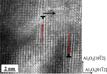
Fig. 8 exhibits a pair of edge dislocations in the sapphire lattice, 20 nm beneath the interface. These dislocations are different from the periodical misfit dislocations shown in the as-grown SOS [Fig. 7(b)]. The latter was formed at the growth process to accommodate the large lattice mismatch through DME.Reference Narayan and Larson17,Reference Bayati, Molaei, Narayan, Narayan, Zhou and Pennycook18 They appear at the interface and are nucleated from the surface steps as shown in Fig. 7(b). In contrast, the implantation-induced dislocations in sapphire lattice were 20 nm away from the interface. These dislocations could be the evidence of the distortion of the sapphire lattice due to excessive Si+ ions since similar defects cannot be found in the as-grown specimen. This supports our deduction and explains why the residual stresses measured are smaller than the calculated thermal stresses.
A high resolution TEM image of the sapphire lattice at the depth of 10–20 nm beneath the interface. The sample was subjected to the 200 KeV and 5 × 10¹⁵ ions/cm2 implantation and 1000 °C annealing.

Finally, our results showed that different annealing temperatures would lead to different interface structures too. Under a low annealing temperature (say 600 °C), the interface still carries the memory of the implanted structure and remains amorphous, as shown in Fig. 7(d). This amorphous region acts as a buffer layer to accommodate the lattice mismatch strain. A sufficiently high temperature of 1000 °C could restore well the crystalline structure of the interface, making it similar to that of the as-grown film [Fig. 7(b)]. The lattice and misfit dislocations could be clearly discerned under the high-resolution TEM [Fig. 7(f)].
V. CONCLUSIONS
Through a comprehensive residual stress characterization and microstructural analysis, this paper has successfully identified the origin of the residual stress variation in SOS thin film systems caused by implantation and annealing. The investigations have led to the following conclusions:
(1) A higher implantation energy and dose density give rise to more reductions of residual stresses because of deeper penetration and more collisions with the lattice atoms.
(2) A sufficiently large implanting energy and dose density can maximize the structural amorphization, and allow the subsequent annealing to render a much better crystal quality of less defects.
(3) Annealing will restore the magnitudes of residual stresses. A higher annealing temperature brings about severer residual stress regeneration. After the annealing at a temperature (1000 °C in the present study) above the film deposition temperature (900 °C in the present study), the as-grown residual stresses were restored in most of implanted samples.
(4) Ion penetration into the sapphire substrate causes its lattice to expand. A subsequent annealing can hardly change it. Hence, after annealing, the ideal crystal quality and the reduced residual stress can both be obtained at the same time by making use of this effect.
ACKNOWLEDGMENTS
This work was sponsored by the Australian Research Council (ARC). Australian National Fabrication Facility (ANFF) provided assistance to the experiments.