I. INTRODUCTION
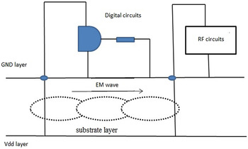
In mixed-signal systems, noise coupling between different domains, such as digital and RF can be a critical problem. When a common power supply is used to power the digital and RF circuits, the power and ground planes in the package can be a major source of noise coupling. Simultaneously switching the drivers may cause voltage fluctuations, which can propagate both horizontally and vertically between power and ground planes. In Fig. 1, the switching digital circuits cause an electromagnetic wave to propagate between the power and ground planes, which can couple to the RF circuits. Therefore, the sensitive RF/Analog signals have to be isolated from this digital switching noise. Hence, the plane structure must be suitably modified such that the substrate coupling should be minimized [Reference Swaminathan and Ege Engin1, Reference Van Den Berghe, Olyslager, De Zutter, De Moerloose and Temmerman2].
Switching noise coupled to RF circuits in mixed-signal systems.

There are two possible ways to reduce simultaneous switching noise (SSN). The first way is keeping the power distribution network (PDN) impedance very low for a wide range of frequencies except DC by means of decoupling capacitor, which is placed between power and ground planes in a package or PCB level [Reference Hubing, Drewniak, Van Doren and Hockanson3–Reference Fan, Cui, Drewniak, Van Doren and Knighten5]. Decoupling capacitor provides low impedance path between power and ground plane to SSN. Thus, it makes the PDN impedance very low. Low impedance PDN can provide the required transient current immediately to the switched transistors and eliminate the noise from spreading throughout the whole PDN. The major drawback of this method is that the decoupling capacitor will become inductive and ineffective in reducing SSN above the self-resonance frequency.
Another isolation method to reduce SSN propagation is to keep part of the PDN at high impedance. The typical isolation methods include etched slots on power/ground planes [Reference Chen, Hubing, VanDoren and DuBroff6–Reference Lee, Rotaru, Iyer, Kim and Kim9], a π-filter with beads [Reference Kim, Lee, Kim and Kim10], or electromagnetic bandgap (EBG) structures [Reference Abhari and Eleftheriades11–Reference Shi and Zhou28]. Using isolation slots on the power or ground planes is one of the effective methods for noise isolation, but it lacks DC connection [Reference Wu, Chen, Hwang and Lin8]. A narrow conducting trace, called bridge, is used to connect two sides of the PDN for DC connection, but the isolation performance degrades at low frequencies [Reference Wu, Chen, Hwang and Lin8]. A π-filter consists of one SMT ferrite bead in series and two SMT decoupling capacitors in parallel are used to replace the narrow bridge in the isolation slots to suppress SSN. Ferrite bead provides DC connection between two sides of the slot and noise isolation is improved by π-filter in the frequency range, where SMT components are still effective.
One of the most promising solutions for noise suppression is applying EBG structure on a PDN. This structure comprises power and ground plane layers separated by a dielectric material. One of the layers consists of EBG structure and the other layer is a continuous metal plane. Single unit-cell of the EBG structure is periodically patterned on a power plane in both x- and y-directions, to provide high-impedance surface. It is called as two-dimensional (2D) EBG structure. The inherent stopband nature of EBG suppresses the noise propagation between power and ground planes. Noise suppression is omni-directional i.e., it suppress the noise propagation in all directions irrespective of the noise source excitation location. The isolation (insertion loss) of the stopband increases while increasing number of unit cells. Ideally, the isolation becomes infinite for infinite number of unit-cells. But, in reality, an isolation of −30 dB could be possible for few unit cells on a PDN. EBG structures can be created at a low cost using standard PCB fabrication processes.
Earlier, these EBG structures were embedded between power and ground planes, and which increased the cost of fabrication and complexity [Reference Abhari and Eleftheriades11]. Therefore, planar EBG structures were used for SSN suppression in mixed-signal systems and high-speed digital circuits [Reference Shahparnia and Ramahi12–Reference Wang, Hsieh, Chuang and Wu16]. The present work proposes a novel planar EBG structure called T-bridge EBG for suppressing SSN on the power/ground planes. This paper is organized as follows: Section II discusses the design concept and characterization of T-EBG structure. The characterization of T-EBG includes the bandgap behavior, significance of increasing the number of unit cells, omni-directional suppression, and the effect of scaling down the physical layout. Section III proposes a novel layout methodology to enhance the bandgap of the proposed T-EBG structure. All the simulated results are verified with the measurement results. Finally, conclusions are drawn in Section IV.
II. DESIGN CONCEPT AND CHARACTERIZATION OF T-EBG
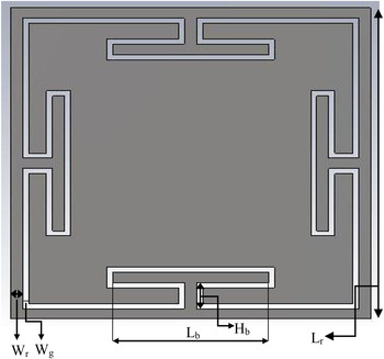
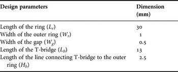
Figure 2 shows the proposed T-bridge EBG unit-cell layout configuration. Physical dimension of the design parameters are shown in Table 1. The area of single unit-cell is 30 × 30 mm2. Length (L r ) and width (W r ) of the outer ring are 30 and 1 mm. Single unit-cell consists of broad metallic patch at the center surrounded by an outer ring, which is used to connect T-bridges on the four sides of the unit-cell. There is no DC continuity between the center patch and the outer ring. A gap (W g ) of 0.5 mm separates the outer ring from the center patch. It is used to increase the effective capacitance of the single unit-cell. Length (L b ) of the T-bridge is 13 mm and the length (H b ) of the line connecting T-bridge to the outer ring is 2.5 mm. T-bridges are used to increase the length of current path in the outer ring. It will increase effective inductance and the center patch is added to introduce the capacitive effect to the single unit-cell of T-EBG. Both the equivalent inductance and capacitance form a parallel resonant circuit. At the resonant frequency, parallel L and C act as an open circuit. Thus the single unit-cell exhibits bandgap characteristics at this resonant frequency. The increase in the number of unit-cells causes the bandgap to increase. Hence, the proposed T-EBG structure suppresses the flow of surface current over the bandgap frequencies.
Unit cell of T-EBG.

Physical dimension of T-EBG.

A) Bandgap behavior of T-EBG
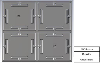
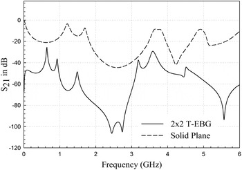
Figure 3(a) shows the layout of T-EBG power/ground plane pair. Four unit-cells are patterned over FR4 substrate (ε r = 4.3, tanδ = 0.025). The substrate thickness is d = 0.8 mm and the metal thickness is 17 µm. The layout size is (60 × 60) mm2. The layer stack-up is shown in Fig. 3(b). There are two ports namely, port-1 which is located at (15,45) and port-2 located at (45,15). The narrow gap between the center patch and outer ring could introduce DC discontinuity between successive unit-cells. So, port-1 and port-2 are completely isolated from common power supply. Port-1 and port-2 typically represent the placement of Analog/RF ICs and Digital ICs. Because of the DC discontinuity, a separate power supply is needed to power up both analog and digital modules. Port-1 is excited for a broad frequency range and the response is observed at port-2. Scattering parameter simulations are performed using 3D full-wave commercial software CST studio suite [29], to find the insertion loss (S 21(dB)) between port-1 and 2. The scattering parameter results for 2 × 2 T-EBG and solid plane (both power and ground planes are continuous) are shown in Fig. 4. The 2 × 2 T-EBG patterned power/ground plane pair has efficiently suppressed SSN propagation compared with solid plane over the frequency range 0.94–3.2 GHz. The lower and upper frequency limit is defined by the insertion loss lower than −40 dB. The difference between these two frequency limit is called as bandgap of T-EBG structure. The simulated bandgap is 2.26 GHz. Thus, the proposed 2 × 2 T-EBG layout provides a perfect isolation between these two ports for the above mentioned frequency range.
(a) Layout of 2 × 2 T-EBG (top-view); (b) layer stack-up.

Simulated insertion loss results of 2 × 2 T-EBG and solid plane.

B) Significance of increasing unit-cells
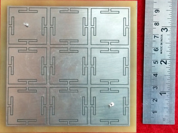
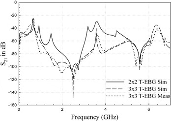
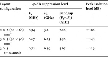
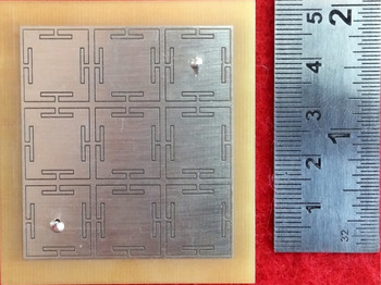
The impact of increasing the number of unit cells on bandgap is studied by comparing the insertion loss characteristics of 2 × 2 and 3 × 3 T-EBG structures. The fabricated 3 × 3 T-EBG is shown in Fig. 5. Figure 6 shows the insertion loss characteristics of 2 × 2 and 3 × 3 T-EBG layout. Agilent N5230A – Network Analyzer is used to measure the insertion loss of the proposed 3 × 3 T-EBG layout. The 85052D (3.5 mm) calibration kit has been used for initial calibration test such as open, short and load conditions. Then, initial calibration kit is replaced with DUT to perform insertion loss measurements. The connector type used in the measurement is straight panel receptacle jack, flange mount. The bandgap range and peak isolation at the center frequency are shown in Table 2 and from the table, it is inferred that the magnitude of both the parameters will increase while increasing the number of unit cells. The bandgap range and peak isolation of 3 × 3 T-EBG are increased by 3.3 and 42 dB, respectively, compared with 2 × 2 T-EBG layout. The measured results have good correlation with the simulated results.
Fabricated 3 × 3 T-EBG layout.

Simulated and measured results of 2 × 2 and 3 × 3 T-EBG.

Bandgap and peak isolation of 2 × 2 and 3 × 3 T-EBG.

C) Omni-directional suppression
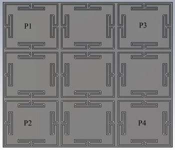
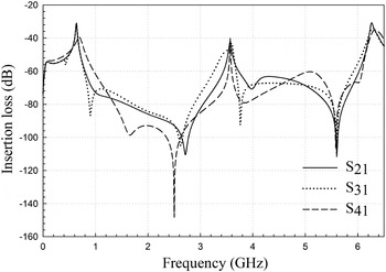
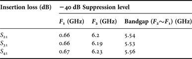
In the previous section, it is shown that the T-EBG structure suppresses the noise propagation between the two ports for the specified bandgap frequencies. This section will address the omni-directional noise suppression behavior of 3 × 3 T-EBG. To verify the omni-directional suppression, noise excitation located at different locations such as port-2, 3, and 4, respectively. The receiving port is all at port-1. The port locations and the physical layout are shown in Fig. 7. The simulated insertion loss results are shown in Fig. 8. Table 3 summarizes the bandgap range of simulated T-EBG structures. It is clearly seen that the noise suppression bandgap is almost same for different locations of noise source excitation. Thus, the proposed T-EBG layout eliminates switching noise omni-directionally.
3 × 3 T-EBG layout configuration in CST studio suite for omni-directional noise suppression simulation.

Simulated insertion loss results of 3 × 3 T-EBG layouts with noise source excited at different port location.

Bandgap range for omni-directional noise suppression.

D) Scaling of T-EBG
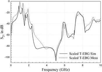
This section will address the scaling of T-EBG and its effect on bandgap response. The T-EBG is scaled down in both X- and Y-directions (thickness remains unchanged). The scaling factor is 0.5. The fabricated T-EBG structure and its insertion loss characteristics are shown in Figs 9 and 10. From Fig. 10, it is seen that the measured insertion loss response has good correlation with simulated results. The bandgap is shifted to higher frequency range due to scaling of T-EBG. An isolation level of −40 dB is observed over the frequency range from 2.22 to 7.19 GHz. The bandgap variation of scaled T-EBG is less than 10% compared with its un-scaled version. Hence, it is inferred that the bandgap is shifted to higher frequency region due to size miniaturization.
Fabricated scaled version of 3 × 3 T-EBG layout.

Simulated and measured results of scaled 3 × 3 T-EBG layout.

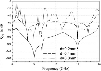
To study the effect of thin substrate on bandgap, scaled T-EBG is simulated for different dielectric thickness such as 0.8, 0.4, and 0.2 mm. The insertion loss results are shown in Fig. 11. Noise suppression level and the corresponding bandgap range are shown in Table 4. From Table 4, it is evident that the bandgap of T-EBG is progressively improved, when the thickness of FR4 is reduced from 0.8 to 0.2 mm. A wide bandgap of 20 GHz is observed for T-EBG patterned over 0.2 mm FR4 substrate. The bandgap is defined as the range of S 21 lower than −60 dB isolation level. The reason for wide bandgap is due to increase in the overall capacitance of T-EBG when reducing the thickness of FR4 substrate. The increase in the capacitance will absorb more electric field inside the FR4 substrate. So, the electric field does not propagate from one port to another. It will cause an increase in the insertion loss between two ports on the T-EBG power plane.
Insertion loss results of T-EBG for different values of dielectric thickness.

Bandgap range of T-EBG for different values of dielectric thickness.

III. COMBINED LAYOUT METHODOLOGY TO ENHANCE BANDGAP
From the literature [Reference Wu, Lin, Wang, Wang and Chen17–Reference Shi and Zhou28], few modifications have been made in the power plane layout to improve the bandgap of EBG structures. LPC EBG [Reference Wu, Lin, Wang, Wang and Chen17] and L-bridge EBG [Reference Wu, Wang, Lin, Wang and Chang18] structures were proposed to obtain a bandgap of 4 GHz. Both the structures were fabricated using standard PCB fabrication process. In [Reference Lee, Kim and Kim19, Reference Mohajer-Iravani and Ramahi21] EBG is patterned over high ε r thin film substrate and high-k dielectric substrate. The observed bandgap ranges are 3.3 and 10.4 GHz, respectively. From [Reference Joo, Kim and Lee20, Reference Kim and Schutt-Aine23, Reference Choi, Govind, Swaminathan and Bharath25, Reference Rao and Swaminathan26] different EBG structures were proposed such as S-bridge, Hybrid Planar EBG, AI-EBG, and AI-EBG with multiple slits. A maximum bandgap of 8 GHz is observed from [Reference Choi, Govind, Swaminathan and Bharath25]. Ultra-wide band suppression of switching noise is proposed in [Reference Qin, Ramahi and Granatstein22, Reference Li, Chen, Yuan and Sawaya24, Reference Bait-Suwailam and Ramahi27, Reference Shi and Zhou28]. A broad bandgap of 15.5 GHz is observed from [Reference Shi and Zhou28]. For ultra-wide band applications, the thickness of the dielectric plays a major role in determining wider bandgap response.
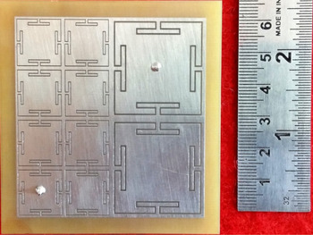
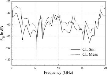
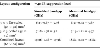
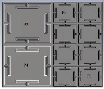
In the present work, a novel layout method has been proposed to broaden the bandgap of T-EBG. The proposed layout is a combination of original layout and its scaled version. The fabricated layout and its insertion loss characteristics are shown in Figs 12 and 13. The simulated results have good correlation with the measurement results. An isolation level of −40 dB is observed over the frequency range from 2.02 to 18.84 GHz. Table 5 summarizes the bandgap range of simulated and measured 3 × 3 un-scaled, scaled versions, and combined T-EBG layout. From Table 5, it can be noted that the combined layout method exhibits broad bandgap compared with other layouts such as un-scaled and scaled T-EBG.
Fabricated combined T-EBG layout.

Simulated and measured results of combined T-EBG layout.

Simulated and measured bandgap comparison of 3 × 3 un-scaled, scaled, and combined T-EBG layout.

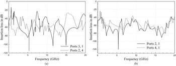
The combined layout is not a periodic structure. So, the bandgap characteristics may depend on the location of noise source input and output ports. To study the bandgap reliance on port location, the input and output ports are considered from different unit-cells of combined layout T-EBG. Four different combinations of port placements are considered in the CL T-EBG such as both ports are located in un-scaled/scaled T-EBG, either one of the port from un-scaled and another from scaled T-EBG and vice-versa. The port locations are shown in Fig. 14. The insertion loss results are shown in Figs. 15(a) and 15(b). Figure 15(a) shows the insertion loss between two ports in the same T-EBG configuration and Fig. 15(b) shows for different T-EBG configuration. The bandgap ranges are shown in Table 6. From Table 6, dual bandgap responses are obtained for S 24, S 31, S 41, and a single broad bandgap for S 21. The average sum of bandgap 1 and 2, for S 24 and S 31 is 13.5 GHz and for S 41 and S 21 is 17.7 GHz, respectively.
Port location in combined layout T-EBG.

(a) Insertion loss response for both ports located in un-scaled/scaled T-EBG. (b) Insertion loss response for ports located in un-scaled and scaled T-EBG.

Bandgap range of CL T-EBG for different location of ports.

From Section II, single bandgap response has been obtained for un-scaled and scaled version of T-EBG. A dual bandgap response is noticed, when both the T-EBG configurations are combined together, one from lower frequency band and the other from higher frequency band. A much broader bandgap response is obtained, when the two ports are located at different T-EBG configuration as well as spaced apart. From Table 6, location of port 1 and 2 are the optimal location to suppress the noise for broad frequency range.
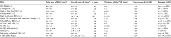
Table 7 shows the comparison of the performance metrics of existing EBG structures with the proposed T-EBG. The performance metrics are total area of EBG patterned layout, area of unit-cell, ε r value, thickness of the substrate, noise suppression level, and bandgap. From Table 7, it is seen that compared with other EBG structures, the proposed combined layout T-EBG provides a broad bandgap with moderate suppression level and takes up less area in the PCB for efficient suppression of simultaneous switching noise.
Performance comparison of CL T-EBG with the existing EBG structures.

IV. CONCLUSION
In this paper a novel EBG structure has been proposed to suppress the simultaneous switching noise for mixed-signal system applications. The proposed T-EBG is patterned over 0.8 mm FR4 substrate, which is easily available and a standard PCB fabrication process is used to realize the proposed layout. So, the fabrication cost is very low. The 3 × 3 T-EBG provides −40 dB isolation over the frequency range 0.72–6.39 GHz. The isolation band covers all the commercial applications such as PCS, GSM, UMTS, CDMA, WLAN, Bluetooth, WiFi, Zigbee etc., Scaling of T-EBG shifts the bandgap towards higher frequency range. As a result, miniaturization is one of the possible solutions to alter the bandgap towards higher frequencies. A study on variation in the thickness of the scaled T-EBG is used to improve the noise suppression level and to increase the bandgap range up to 20 GHz. The proposed combined layout occupies less space (60 × 60) mm2 and provides an isolation level of −40 dB from 2.02 to 18.84 GHz. The placement of the port will determine the bandgap frequency range in CL T-EBG. For UWB applications, the combined layout T-EBG will provide better isolation between RF/Analog and digital circuits. The simulated results are verified with the measured results and a good accuracy is maintained between them.
 Vasudevan Karuppiah completed his B.E in Electronics and Communication Engineering from PSNA College of Engineering and Technology in the year 2002 and M.E in Wireless Technologies in 2005 from Thiagarajar College of Engineering, Madurai, Tamilnadu, India. He is pursuing Ph.D. degree in the field of electromagnetic interference in high speed digital systems. His research interests include Computational methods for EMI/EMC, Signal integrity issues in high speed digital systems.
 Raju Srinivasan completed her B.E in Electronics and Communication Engineering from P.S.G college of Technology in the year 1982 and M.E in Communication systems in 1984 from Regional Engineering College Trichy, India. She obtained her Ph.D. in the area of Microwave integrated circuits in the year 1996 from Madurai Kamaraj University. She has co-authored 47 technical papers in international and national journals. She has published 60 papers in international and national conferences. Her research interests include Computational electromagnetics, Modeling and Optimization of RF systems and Antenna.