Amorphous metal oxide semiconductors have attracted much attention as candidates for the backplanes of active-matrix organic light-emitting diode displays owing to their high field-effect mobility.[Reference Nomura, Ohta, Takagi, Kamiya, Hirano and Hosono1] To date, outstanding progress has been made in the area of solution processing for oxide semiconductors, [Reference Adamopoulos, Bashir, Wobkenberg, Bradley and Anthopoulos2–Reference Banger, Yamashita, Mori, Peterson, Leedham, Rickard and Sirringhaus4] as researchers attempt to meet the requirements of low-cost fabrication and printed electronics. Recently, a high-performance InZnO semiconductor fabricated under 250 °C using metal alkoxide precursors was reported.[Reference Banger, Yamashita, Mori, Peterson, Leedham, Rickard and Sirringhaus4] However, fabrication steps requiring anhydrous conditions are very expensive and complicated.[Reference Brinker and Scherer5] Recently, solution processed ZnSnO (ZTO) thin films have been investigated for low-cost fabrication of oxide thin-film transistors (TFTs). Amorphous ZTO semiconductor exhibits excellent semiconducting properties and enables low-cost fabrication without an indium composition.[Reference Chiang, Wager, Hoffman, Jeong and Keszler6] The conventional solution process for producing ZTO semiconductors utilizes a non-aqueous solvent such as acetonitrile or 2-methoxyethanol and metal chloride precursors. However, non-aqueous solutions with chloride precursors have a high decomposition temperature of more than 400 °C in order to obtain good electronic characteristics and also effect of chlorine residue is vague.[Reference Avis and Jang7, Reference Seo, Hwang and Bae8]
In this study, we report a low-temperature-processed, novel fluorine-doped zinc tin oxide (ZTO:F) TFT using a simple aqueous solution process. The aqueous solution process utilizing rapid hydrolysis and condensation reactions enables the low-energy kinetics of M-O-M network formation without any organic residues. In particular, we emphasize that the overall fabrication cost is cheap for several reasons: (i) the process uses an inexpensive solvent (water) and affordable metal precursors and (ii) all ZTO:F film fabrication steps including stirring, spin coating, and annealing were performed under ambient air conditions. The ZTO:F TFT with fluorine of more than 5%, which was annealed at low temperature of 250 °C in an ambient atmosphere, shows a field-effect mobility of 2.85 cm2/V s and ΔV th of less than 1.73 V under long-term positive bias stress. We conjecture that fluorine, which has similar ionic size with oxygen, is responsible for the enhanced electrical characteristics of the suggested ZTO:F TFT. Specifically, the different electrovalency of fluorine as compared to oxygen offers more n-type carriers and passivates oxygen vacancy diffusion well via the formation of metal fluoride bonds at the channel/gate dielectric interface.
To synthesize the aqueous ZTO:F solution, tin fluoride (SnF2) and zinc fluoride hydrate (ZnF2·xH2O) were used as fluorine-providing precursors. A 0.2 M aqueous solutions of ZTO:F was synthesized by dissolving SnF2 and ZnF2·xH2O powders (Sigma-Aldrich, St. Louis, MO) in water mixed with various ZnF2:SnF2 molar ratios appropriate to the desired product composition. All prepared solutions were stirred to ensure complete mixing of the solutions in a glass vial at ambient temperature for 4 h. The pH of ZTO:F aqueous solution is 5.297 at 26.0 °C. For fabrication of the ZTO:F TFT, SiO2/p+-Si substrates were used as gate dielectrics/gate. The ZTO:F solution was spin coated on the substrate at a speed of 5000 rpm for 30 s. Then, the ZTO:F/SiO2/p+-Si substrates were kept at 250–500 °C on a hotplate in ambient air so that less than 10 nm of ZTO:F semiconductor thin films were obtained. A total of 100 nm Al source and drain contacts were then deposited by an E-beam evaporator on top of the metal oxide layer through a shadow mask. The evaporated channel length and width were 100 and 1000 µm, respectively. Structural and chemical properties of the ZTO:F thin films were analyzed by x-ray diffraction (XRD), atomic force microscopy (AFM), scanning electron microscopy (SEM), and x-ray photoelectron spectroscopy (XPS). TFT characterization was performed at room temperature with an HP 4156A semiconductor parameter analyzer. Measurements were typically made in continuous mode, with the transfer curve recorded before the output curve. Bias stability tests were performed at room temperature and a constant current of 10 µA (V DS = 20 V) and a gate bias of 10 V for 0–3600 s.
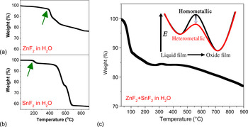
Figure 1 displays the thermogravimetric analysis (TGA) results of aqueous metal fluoride solutions measured under dry air atmosphere. In the TGA of aqueous ZnF2 solution [Fig. 1(a)], the first decomposition observed at 400 °C is attributed to the decomposition of Zn(OH)F to form ZnO and ZnF2. Also, ZnF2 can be hydrolyzed by the water traces, which leads to the formation of oxides, or volatilized as indicated by the continued weight loss at temperature exceeding 500 °C.[Reference Srivastava and Secco9] In the TGA of the SnF2-based aqueous solution [Fig. 1(b)], the thermal decomposition is observed at a lower temperature (200 °C), which can be attributed to the high solubility of SnF2 in water.[Reference Seby, Potin-Gautier, Giffaut and Donard10] We then characterized the TGA of the mixed aqueous ZnF2–SnF2 solution [Fig. 1(c)]. Intriguingly, rapid thermal decomposition is observed at temperature below 100 °C; this corresponds to the evaporation of water traces produced during condensation of the two different metal monomeric species. In correlation with the high decomposition temperature of each metal monomeric species, the decomposition of aqueous ZnF2–SnF2 solution at low temperature (<100 °C) indicates that the reaction between each metal monomeric species to form hetero-metallic oxide derivatives is dominant over their self-condensation [Eqs. (1) and (2)]. This can be attributed to a nucleophilic reaction between two different metal monomeric species, which occurs as a result of the difference in electronegativity between the species.[Reference Niederberger and Pinna11] SnF2 is easily hydrolyzed to form Sn(OH)F or Sn(OH)2 due to the high solubility of SnF2 in water:[Reference Tsukuma, Akiyama and Imai12]


TGA of (a) aqueous ZnF2 solution, (b) aqueous SnF2 solution, and (c) aqueous ZTO:F solution. An initial weight loss point of the ZnF2 solution and the SnF2 solution is at around 400 and 200 °C, respectively. However, continuous weight loss is shown at room temperature to 230 °C in the ZTO:F solution. Self-condensation of different metal species in ZTO:F solution lowers kinetic energy for oxide networks and decreases decomposition temperature.

M-O-M networks originate from a nucleophilic reaction between different metal monomeric species in the aqueous solution. Conventional method usually forms M-O-M networks during annealing through the interaction between a coated liquid film and water molecules in ambient air.[Reference Lee, Chang, Herman and Chang13] In this study, hydrolysis and condensation reaction in aqueous solution already form M-O-M networks so that can lower kinetic energy to obtain oxide materials during annealing, resulting in low processing temperature of 250 °C as shown in the inset of Fig. 1(c).
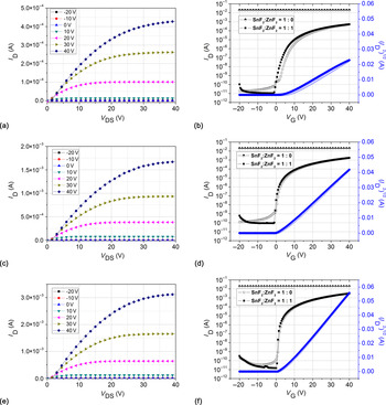
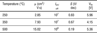
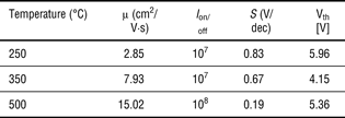
Figure 2 displays the electrical properties of ZTO:F TFTs annealed at 250 °C for 12 h, 350 °C for 1 h, and 500 °C for 1 h. In Fig. 2(b), the transfer curve for the ZTO:F TFTs with a molar ratio of SnF2:ZnF2 = 1:0, which is a pure F:SnO2, shows a normally on state current against the gate voltage, indicating conductor-like behavior. The ZTO:F TFT with SnF2:ZnF2 = 1:1, which is the optimized composition, ZTO:F TFT annealed at 250 °C shows a high field-effect mobility of 2.85 cm2/V s, an on-to-off current ratio of more than 107, and a sub-threshold swing of 0.83 V/dec. The aqueous solution processed ZTO:F TFTs show outstanding electrical properties, as presented in Table 1. It is well known that a ZTO system with Sn:Zn = 1:1 effectively forms an amorphous phase by distortion of the lattice sites driven by the substitution between Zn and Sn.[Reference Hayashi, Kondo, Murai, Moriga, Nakabayashim, Fukumoto and Tominaga14] Also, the resistivity increases as ZnO increases in the amorphous ZTO:F films because the oxygen vacancies are reduced due to the higher bonding energy of Zn–O than Sn–O. Thus, the transition to a semiconducting state of the optimized ZTO:F TFT can be explained by the decreased carrier concentration, resulting from the suppression of oxygen vacancies.[Reference Seo, Choi, Hwang and Bae15–Reference Jeong, Bae, Kim, Song, Woo, Shin, Cao and Moon17]
Output curves of ZTO:F TFTs annealed at (a) 250 °C for 12 h, (c) 350 °C for 1 h, and (e) 500 °C for 1 h. Transfer curves of ZTO:F TFTs annealed at (b) 250 °C for 12 h, (d) 350 °C for 1 h, and (f) 500 °C for 1 h.

Electrical properties of ZTO:F TFTs annealed at 250 °C for 12 h, 350 °C for 1 h and 500 °C for 1 h.
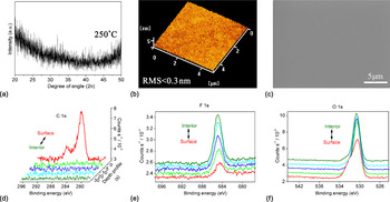
The microstructure of the ZTO:F thin film was analyzed with the aid of XRD, SEM, and AFM. The ZTO:F film has an amorphous phase and a smooth surface. The surface roughness of the ZTO:F TFT fabricated at 250 °C is 0.4 nm. It can thus be surmised that there is no corrosive attack on the SiO2/p+-Si substrate by the acidic ZTO:F precursor solution. Also, the chemical bonding structure and the atomic composition of the ZTO:F film were investigated by XPS. The XPS binding energies of the ZTO:F film surface was referenced to the C1s peak of hydrocarbon contamination at 285.0 eV while the Ar 2p3/2 peak at 242.0 eV was referenced in order to define the interior of the ZTO:F film after sputtering by Ar bombardment for 30 s.[Reference Oswald and Baunack18] As shown in Fig. 3(d), there are no carbon-related organics in the interior of the ZTO:F thin film, and that the thin film was successfully doped, as evidenced by the F1s peak at 684.9 eV in Fig. 3(e). The value of the F1s peak in the ZTO:F thin film could be defined by the coordinated environment around fluorine, mainly Sn–F[Reference Martinez, Huerta, O-Rueda de Leon, Acosta, Malik and Aguilar23] or Zn–F[Reference Kawamoto, Ogura, Shojiya, Takahashi and Kadono24] bonds in oxide networks. The fluorine content of the ZTO:F film increases from 2.21% at the surface to 6.35% in the interior. Beyond 5% F doping content inside the ZTO:F channel, the ZTO:F TFT shows a small sub-threshold swing (S) and hysteresis between forward and backward bias. Consequently, it can be concluded that F atoms chemically bonded well with metal cations and an organic residue-free amorphous ZTO:F thin film was successfully fabricated at low temperature.
(a) Amorphous structure, (b) smooth surface, and (c) uniformity analyzed by XRD, AFM, and SEM, respectively. (d) C1s, (e) O1s, and (f) F1s XPS results of ZTO:F thin film fabricated at 250 °C for 12 h.

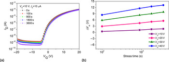
Figure 4 displays the threshold voltage shift (ΔV th) of the ZTO:F TFT under long-term positive bias stress. The ZTO:F TFT fabricated at 250 °C was stressed for application to the backplanes of an active-matrix organic light emitting diode (AMOLED) under conditions of a constant current bias with 10 µA and gate voltage bias with 10 V for 100, 900, 1800, and 3600 s at room temperature. The ZTO:F TFT showed a relatively low positive ΔV th, as small as 1.73 V, after application of bias stress for 1 h. ΔV th under higher gate voltage bias shows higher threshold voltage shift due to larger trap density as shown in Fig. 4(b). These results are comparatively better than those of other ZTO TFTs fabricated by organic solution process.[Reference Avis and Jang7, Reference Seo, Choi, Hwang and Bae15–Reference Jeong, Bae, Kim, Song, Woo, Shin, Cao and Moon17] Bias instability of oxide TFTs under positive bias stress usually originates from electron trapping due to O2 adsorption to the channel surface[Reference Jeong, Yang, Jeong, Mo and Kim19] and defects in the film or at the channel/gate dielectric interface.[Reference Nomura, Kamiya, Hirano and Hosono20] In fact, it is not clear as to whether the ΔV th originates from O2 adsorption at the surface of the ZTO:F channel layer, because the fluorine content is low at the ZTO:F surface, as shown in Fig. 3(e). Notably, Lai et al. reported that a HfO2 gate dielectric with a fluorinated surface can suppress carrier trapping due to oxygen vacancy diffusion along the direction from the gate dielectric to the channel or in the opposite direction.[Reference Lai, Wu, Chao, Chen, Wang, Tany and Rowell21, Reference Tseng, Tobin, Hebert, Kalpat, Ramón, Fonseca, Jiang, Schaeffer, Hegde, Triyoso, Gilmer, Taylor, Capasso, Adetutu, Sing, Conner, Luckowski, Chan, Haggag, Backer, Noble, Jahanbani, Chiu and White22] Therefore, we believe that metal fluoride bonds derived from fluorine content inside the ZTO:F channel passivate oxygen vacancy diffusion at the channel/gate dielectric interface when long-term gate bias is applied to the channel.
(a) Transfer characteristics of ZTO:F TFT with positive threshold voltage shift under gate voltage (V G) of 10 V and constant current bias of 10 µA for 1 h, and (b) threshold voltage shift (ΔV th) as a function of stress time for 1 h. The current bias stress (I DS) is as same as 10 µA, but each gate bias (V G) is different as purple squares (10 V), red diamonds (20 V), green triangles (30 V), and blue circles (40 V).

Amorphous fluorine-doped zinc tin oxide (ZTO:F) TFTs were fabricated via an aqueous solution process using metal fluoride precursors. A nucleophilic reaction between heterometallic species in the aqueous solution enables decreased fabrication temperature of the fluorine-doped oxide film. A ZTO:F TFT fabricated at 250 °C, presenting a smooth surface and little organic residue, showed a field-effect mobility of 2.85 cm2/V s, on-to-off current ratios exceeding 107, and sub-threshold swings of 0.83 V/dec. Also, a small threshold voltage shift of 1.73 V was observed under stress conditions of gate voltage of 10 V and constant current of 10 µA. These unique properties of fluorine allow the realization of high-performance ZTO:F TFTs with potentially important application to practical devices. The process is applicable to a broad range of amorphous metal oxide compositions for application to the backplanes of AMOLEDs and also provides extremely low-cost fabrication.
Acknowledgments
This research was financially supported by the Ministry of Knowledge Economy (MKE) and Korea Institute for Advancement in Technology (KIAT) through the Workforce Development Program in Strategic Technology. This research was also supported by the Basic Science Research Program through the National Research Foundation of Korea (NRF) funded by the Ministry of Education, Science and Technology (MEST) (CAFDC-20100009898).