I. INTRODUCTION
The microstructures of sintered compacts of the transition metal carbides (Ti, V, Cr, Nb, Ta, Zr–C) are often fraught with facetted and abnormal grains. The commercially important monocarbide of tungsten, WC, is also not an exception. This tendency of sintered WC compacts to evolve into a faceted grain structure is generally attributed to the difference in surface energies between the different crystallographic planes. The  $\left\{ {10\bar 10} \right\}$ prismatic planes are kinetically more active than the {0001} basal planes and hence truncated pyramidal or rectangular platelet morphologies are usually observed in sintered compacts that have undergone substantial grain growth.Reference Yuan, Rohrer, Song, Chien and Li1–Reference Li, Shu, Yuan-jie, Xian-wang and Xiang-jun3 Thus, when wetted by liquid metals (for instance by Co or Ni, leading to cemented WC), a vicinal or singular solid–liquid interface develops and coarsening progresses by interfacial control leading to flat interfaces in the sintered compacts. As a consequence of the strong surface energy anisotropy and faceting, abnormal grain growth (AGG) is also frequently observed. Unlike the oxide ceramics like α-Al2O3 which also share this characteristic trait, AGG in WC is generally attributed to the activity of carbon in the sample—a high density of abnormal grains are often observed at the WC/Carbon die interface after a sintering experiment.Reference Cha and Hong4,Reference Girardini, Zadra, Casari and Molinari5 From a fundamental standpoint, AGG is an interesting case of nonlinear crystal growth kinetics and has been well documented and reviewed in both oxides and carbides.Reference Jo, Kim and Hwang6,Reference Kang, Lee and Yan7 This natural propensity of WC (and most of the early transition metal carbides) to undergo faceting and AGG has made them apt systems for both theoretical and experimental studies on unique grain growth phenomena, particularly at high temperatures.
Interestingly, these non-oxide ceramics sometimes also show fully isotropic grain growth (IGG) with selective metalloid additions. A classic example of an IGG inducer is boron, as has been experimentally reported in NbC-BReference Oh, Jun, Kim and Hwang8 and WC-B.Reference Nanda Kumar, Watabe and Kurokawa9 Apparently, a liquid B2O3 oxide phase forms at low temperatures that wet the flat carbidic GBs, leading to GB roughening and IGG at high temperatures.Reference Nanda Kumar, Watabe and Kurokawa9 On the other hand, it has also been recently observed that the addition of a few elements like Ti,Reference Lay and Loubradou10 Si,Reference Nanda Kumar, Watabe and Kurokawa11,Reference Nanda Kumar, Watabe, Yamauchi, Kobayashi and Kurokawa12 or SiCReference Nanda Kumar, Watabe, Yamauchi, Kobayashi and Kurokawa12–Reference Sugiyama, Kudo and Taimatsu14 to WC can also lead to extreme platelet-type abnormal grains that are difficult to control. These platelets in WC with aspect ratios easily exceeding 4–5, are a special type of abnormally grown grains most often (but not necessarily always) comprising of a pair of flat crystals separated by a thin faulted region containing a stacking fault (SF) or a twin defect. A few immediately observable features distinguish them from the previously mentioned abnormal grains in WC that arise from surface energy anisotropy or differences in carbon activity: (i) the platelets are found in the microstructure of the samples and are not localized to the sample/carbon die interface, (ii) most often than not, the platelets occur in pairs, connected by a fault line running parallel to the interface, and (iii) from experimental observations it was found that these platelets too follow similar evolution trajectories as abnormal grains in other oxide systems like Al2O3—namely, their volume fraction increases with the volume fraction of the liquid phase in the system.Reference Nanda Kumar, Watabe and Kurokawa15 Such AGG is difficult to control unless their mechanism and pressure–temperature range of operation are clearly known. Interestingly, the AGG is prominent in nanosized powders where the kinetics is so rapid that grain boundary (GB) migration across the entire length of a grain occurs within a fraction of a minute.
This paper is devoted to a detailed study of the defects and the mechanism of microstructural evolution in sintered nanograined WC–Si cermets, which show extreme AGG. Specifically, two temperatures were chosen for the study: 1323 K to study the microstructure under solid state sintering and 1673 K when the Si has melted to resemble liquid phase sintering (LPS). Although the actual melting point of Si (1687 K) is slightly higher than the LPS temperature used in this work, the lowest eutectic in the W–Si system occurs at 1663 K.
II. EXPERIMENTAL DETAILS
Commercially purchased (M/s. Allied Materials, Japan) nanosized WC powder (70 nm by Brunauer–Emmett–Teller [BET] analysis) was ball milled with 1 wt% Si (∼50 μm) in a planetary ball milling unit for 60 min. Powder compaction was carried out by spark plasma sintering (SPS) using a graphite die with carbon spacers. After an initial presintering hold at 873 K for 3 min, a constant heating rate of 50 K/min and compressive stress of 50 MPa were applied until the end of sintering. For all the experiments, the vacuum level in the chamber before starting the sintering process was maintained below 4 Pa. The first two samples were prepared by isothermal holding at 1323 K for 30 and 60 min, respectively, (to resemble solid state sintering conditions) while the third sample was sintered at 1673 K for 20 min (for LPS conditions). For transmission electron microscopy (TEM) analysis, the samples were first cross-sectioned and subsequently thinned by mechanical polishing, dimpling, and Ar ion milling at 4 kV. For the EBSD analysis, cross-sectioned specimens of the high-temperature sintered sample were polished successively by diamond paste with particle sizes of 1 μm and 250 nm and ultrafine alumina. For the electron back-scattering diffraction (EBSD) scan, a pixel size of 30 nm was used, and spurious pixels were removed using a clean-up routine, available with the OIM analysis software.
III. RESULTS
A. General microstructure evolution
Figure 1 shows the microstructure of the samples sintered at 1323 and 1673 K. At 1323 K, the microstructure is marked by continuous porosity (intermediate stage of sintering) with nanosized WC particles without any AGG. Just below TmSi (1673 K), elongated grains and clusters of faceted grains show up abruptly and persist until the end of sintering. Three distinct features can be discerned in the microstructure: (i) small faceted grains representing a polycrystalline matrix (ii) elongated, strongly faceted, and abnormally grown grains (‘platelets’) and (iii) clusters of small faceted grains with faceted pores packed between abnormally grown grains. The large grains also show intermittent porosity implying that the coarsening rate in the system was far greater than pore closure rates [Fig. 1(c)]. Initially it was suspected that the strong anisotropy of platelets could be induced by differences in coarsening rate constants between the length and width directions of the platelets [as has been reported for certain Si-containing systems like β-Si3N4 (Ref. Reference Lai and Tien16) and SiC] and therefore would hold for isothermal sintering too. However, a systematic analysis conducted to study the growth kinetics of the different facets showed that the coarsening behaviour of the high-temperature platelets, unlike the smaller isotropic grains, cannot be ascribed to any normal growth behaviour (Fig. 2) and that the drastic anisotropy was brought about within the first one minute of sintering at T ≥ 1673 K after which further coarsening is interrupted by the impingement on neighboring grains leading to a tough interlocked microstructure (K Ic measured by indentation cracking exceeded 8 MPa m1/2). Phase analysis by XRD (figure not shown) revealed that silicide compounds, WSi2 and W5Si3, also grew by solid state reactions above 1423 K.
Microstructures of ultrafine WC–Si samples sintered at (a) 1323 K showing a Si particle in the nano grained WC matrix; (b) 1673 K showing clusters and abnormally grown grains with clear crystal facets, and (c) 1673 K sintered specimen showing an abnormal grain with pores arranged along the line of contact of two basal planes. All distance markers represent 1 μm.

Coarsening rate of small grains and platelets at 1673 K.
B. Low-temperature microstructure
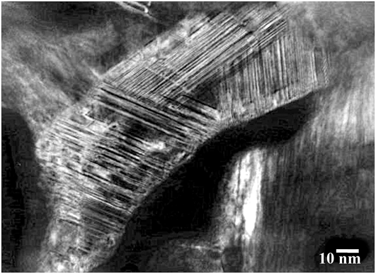
Figure 3 is a TEM micrograph of the low-temperature sintered specimen along with the selected area diffraction (SAD) pattern. Almost the entire microstructure was found to be populated by a very high density of planar defects and extended dislocations. The corresponding electron diffraction patterns showed profuse streaking along  $\vec g = \left\langle {10\bar 10} \right\rangle$ indicating that the planar defects are SFs lying on the prismatic planes of the WC grain. Approximately 8–10 diffraction patterns were recorded from different grains of each specimen. Almost all the faulted grains that were analyzed along various low index zone axes ([0001] and
 $\left[ {11\overline 2 0} \right]$) had the SFs only on the prismatic planes bound by partial dislocations with a Burgers vector (b.v), determined after conventional tilt experiments, of
 ${1 \mathord{\left/ {\vphantom {1 6}} \right. \kern-\nulldelimiterspace} 6}\left[ {\bar 12\bar 13} \right]$ as is commonly observed in indented samples of WC.Reference Hibbs and Sinclair17 Two interesting observations were also recorded in the analyzed diffraction patterns: in some cases, we found that the streaks along
 $\overrightarrow g = \left\langle {10\bar 10} \right\rangle$ converged into fine spots, indicating the formation of nanoscale twins [see Fig. 4(a)] or the occurrence of an ordering of the defect planes. However, these observations were few in comparison with the streaking patterns of the SFs. Also, some faulted grains that showed strong streaking in the diffraction patterns and a high density of SFs were characterized by an intensity maximum exactly midway between two
 $\vec g = \left\langle {10\bar 10} \right\rangle$ reflections [Fig. 4(b)]. This is a signature of the orthorhombic (O-phase) transformation, produced by the passage of
 ${1 \mathord{\left/ {\vphantom {1 6}} \right. \kern-\nulldelimiterspace} 6}\left[ {12\bar 13} \right]$ dislocations on every successive prism plane, as suggested by Jayaram et al.,Reference Jayaram, Sinclair and Rowcliffe18 to explain decarburization in heavily deformed WC–Co carbides. This is an intermediate phase that forms as carbon diffuses out through the SFs to form a secondary carbide that is metal rich (Co–W–C). The local nonstoichiometry in the original WC grain is adapted into a pseudohexagonal structure that is periodically faulted. Such intermediate structures induced by defect-ordering are not uncommon in WC (for instance one SF for every seventh plane has also been reported to form a superstructureReference Zhi-min, Chang-hui, Jun, Daniel, Yannick, Serge and Martin19), as also the formation of nonstoichiometric phases within the faults or at GBs.Reference Gai, Torardi, Boyes, Harris and Edwards20,Reference Gao, Song, Liu, Wei, Wang and Guo21
(Top) (a) BF and SAD pattern of the sample sintered at 1323 K for 30 min obtained with the zone axis close to [0001]; (Bottom) a, b, and c are the centered DF images from the spots marked in the SAD pattern above.
(a) Diffraction from a multiply twinned grain showing matrix (M) and twin (T) reflections as faint spots; (b) SAD pattern from a grain oriented with the incident beam nearly parallel to [0001], showing strong streaking along  $\left\langle {10\bar 10} \right\rangle$. The arrows point to reflection spots in the streaks midway between the primary reflections. These are signatures of the ‘O’ phase.
The sample sintered for 60 min at 1323 K also showed an exactly similar microstructure with respect to the nature of the defects, but with slightly enhanced grain growth (Fig. 5). However, the defect density (number of grains with SFs) was found to be lower, probably owing to the extended annealing period.
TEM micrograph of specimen sintered at 1323 K for 60 min.
Interestingly, in both the low-temperature sintered specimens, pockets of an amorphous carbon-rich phase were also detected in some regions of the microstructure, particularly between heavily faulted grains (Fig. 6). This feature was observed in many areas of the low-temperature sintered specimens and we believe that this is not an artifact of the specimen preparation technique, such as re-deposition which was minimized using a dual gun polishing system. Particle re-deposition during ion milling is evident by the thin amorphous region surrounding almost all the particles, but the graphite-like pockets were quite obvious by the wavy fringe patterns and their extreme transparency to the electron beam. Since the observed regions are from cross-sectioned samples, the carbon must have occurred as a reaction product and cannot be an impurity from the sintering die or spacer. X-ray diffraction (XRD) of the low-temperature sintered specimen (shown in supplementary information, S1) displayed broad peaks at 2θ ≈ 20°, that correspond to carbon and a WCx phase (ICDD Ref. No: 00-020-1314). With the TEM, no diffraction contrast could be observed from these pockets, but analyzing the X-ray signals from the area using the X-ray energy dispersive spectrometer (XEDS) available with the TEM (a probe size of 2 nm and a short collection time of 20 s were used to avoid electron beam induced damage) confirmed these regions to be extremely carbon-rich (amorphous carbon with trace amounts of W and Si), as shown in Figs. 6(a)–(c). It is interesting that a C-rich pocket should form in the microstructure, since the decomposition was not expected thermodynamically at these temperatures. A look at the W–Si–C phase diagram suggests instead that a ternary equilibrium can be established between WC–C–SiC. In a previous report, we had shown that at low temperatures, WC is invariably oxidized to WO3, and W–Si compounds start to nucleate at around 1400 K.Reference Nanda Kumar, Watabe and Kurokawa15 The excess C must then be driven out (decarburized) as either C–O (gas) or must stabilize as C–SiC. It appears that in the present system, the remnant excess carbon stabilizes as almost amorphous Si/W doped carbon layers, with the out-diffusion of C being aided by the large defect density. Owing to the huge difference in size between the WC (<100 nm) and Si (>2–5 μm) particles, only local equilibrium is established at low temperatures; therefore in the vicinity of the Si inclusion, SiC and the silicides form, while away from the Si inclusion, WC and a carbon-rich phase with trace amounts of Si and W form. The nonstoichiometric phases away from the Si inclusion form only when the sample is isothermally held at low temperatures. At higher temperatures, the Si equilibrium follows the tie line: Si → SiC → WSi2 → W5Si3 → WC. In a previous report,Reference Nanda Kumar, Watabe and Kurokawa15 we had shown that this was indeed the case: in the LPS specimen, the Si concentration gradient was clearly observed with the inclusion being converted to SiC and the silicides forming uniformly in the WC matrix. While this observation of a dissociation reaction in WC at such modest temperatures has not been reported previously, the recent spate of reports on the synthesis of graphene and doped graphene by heating such metal carbides to similar temperatures (for instance, boron doped graphene from boron carbide obtained by heating a pellet of B4CReference Vineesh, Praveen Kumar, Takahashi, Kalita, Alwarappan, Pattanayak and Narayanan22) support our observation of a graphitic phase in the microstructure, derived from the carbon out-diffusion through the faults.
BF from the sample sintered at 1323 K, showing a pair of heavily faulted grains. The carbon pocket and pore are marked. The uniform gray contrast appearing at the periphery of the particles to ∼10 nm is an amorphous re-deposit and is an artifact of the milling process. The carbon-rich pocket is distinguished by its uniform gray contrast. The XEDS spectra acquired by cutting down the beam to a 1 nm probe from the regions marked as A, B, and C in the BF are also shown. Note the intensity of the C line relative to W from the amorphous pocket; a trace amount of Si is also expected in this area, since the Si and W lines are within 40 eV of each other.
C. High-temperature microstructure
The LPS compact sintered at 1673 K had a complex microstructure comprising faceted grains, platelets, and clusters. The platelets always comprise a pair of thin crystals joined along the basal planes by a thin SF and bound laterally by the prismatic planes [Fig. 7(a)]. All the abnormally grown grains showed such a crystallographic structure. Examination of a cluster showed a number of faceted crystals packed between larger abnormal grains [Fig. 7(b)]. The cluster is comprised mainly of Σ1 and Σ2 GBs, and such clusters are generally enclosed between large platelets (the Σ2 is a unique GB correlation that arises in WC between two contiguous grains related by a 90° rotation along  $\left[ {10\bar 10} \right]$, since in WC c/a ≈ 1). All the platelets analyzed were also found to be surrounded by a few WSi2 crystals on their basal planes.
(a) BF of a platelet from the specimen sintered at 1673 K. The inset shows the SAD obtained from  $\approx \left[ {11\overline 2 0} \right]$ zone axis. WSi2 forms on the basal plane of the abnormal grain; (b) BF of a cluster of faceted grains from the same specimen.
To analyze the high-temperature microstructure further, EBSD analysis was carried out. Figures 8(a) and 8(b) show the GB and inverse pole figure (IPF) maps of the LPS sample. EBSD was carried out on polished cross-sections of the pressed pellets and hence represent the microstructural texture viewed normal to the compression axis. Clearly, the rod-like grains in the IPF arise from poles around  $\left[ {10\bar 10} \right]$ and
 $\left[ {2\bar 1\bar 10} \right]$. The GB map showed both low angle (LA) GBs (<5°) and high angle (HA) random GBs. The carbide/carbide GB orientation texture was further analyzed by studying the misorientation distribution function (MDF), which refers to the occurrence of various angular rotations between contiguous grains along three principal crystallographic axes, in axis-angle representation. Figure 9 shows the MDF plotted in axis-angle space for different misorientation angles from 1° to 90°. The LAGBs (with LA misorientations), as seen from the highly populated MDF plot, seem to be distributed among the
 $\left\{ {0001} \right\}$,
 $\left\{ {10\bar 10} \right\}$, and the
 $\left\{ {2\bar 1\bar 10} \right\}$ poles but with propensity for small rotations around the
 $\left[ {0001} \right]$ axis. This might suggest clustering of small facetted grains with low misorientation angles (<1°) around the c axis, leading to growth by coalescence. However, for rotations of 90°,
 $\left[ {10\bar 10} \right]$ is the dominant misorientation axis of the GBs (corresponding to the Σ2 boundary). The low c/a ratio of WC allows these types of special GBs to form preferentially in sintered compacts.
(a) GB map showing the WC grains and both HA (red) and LA (green lines) GBs (LA GBs are marked by yellow arrows) and (b) IPF map from the same area.
Distribution of the misorientation angles of the sample sintered at 1673 K. The 90° rotation clusters around  $\left\{ {10\bar 10} \right\}$, indicating a Σ2 GB.
These observations strongly indicate that the high-temperature normal grain growth may be controlled to a large extent by coalescence of low surface energy boundaries, by small and random rotations of adjacent grains along either the basal or prismatic axes.
IV. DISCUSSION
WC has a hexagonal close packed unit cell (space group: P-6m2) with c/a = 0.976 with alternate prism planes having similar carbon co-ordination. The  $\left\{ {10\bar 10} \right\}$ prism planes are the usual glide planes in hexagonal crystals and the defects in WC, particularly, deformation defects like SFs are also generally reported to be formed on the prismatic planes.Reference Hibbs and Sinclair17,Reference Bolton and Redington23 Through observations of indented samples, it has been established that the SF forms by the dissociation of a single slip dislocation with a b.v of
 ${1 \mathord{\left/ {\vphantom {1 3}} \right. \kern-\nulldelimiterspace} 3}\left[ {\bar 12\bar 13} \right]$—the ribbon of SFs being enclosed by two partial dislocations of equal b.v,
 ${1 \mathord{\left/ {\vphantom {1 6}} \right. \kern-\nulldelimiterspace} 6}\left[ {\bar 12\bar 13} \right]$ on the prismatic planes. The low stacking fault energy (γ), between 50 and 180 mJ/m2 (through experimental and theoretical measurements), permits the leading and trailing partials to be widely separated.Reference Hibbs and Sinclair17,Reference Greenwood, Loretto and Smallman24,Reference Nabarro, Bartolucci Luyckx and Waghmare25 On the other hand, the high temperature platelets have characteristic fault lines on the basal plane of the
 ${{\left\langle {01\bar 10} \right\rangle } \mathord{\left/ {\vphantom {{\left\langle {01\bar 10} \right\rangle } {\left\{ {0001} \right\}}}} \right. \kern-\nulldelimiterspace} {\left\{ {0001} \right\}}}$ type, although the applied stress was the same throughout the experiments. SFs on the basal planes in WC are rare since the slip system usually involves the prismatic planes. However, deformation SFs involving the basal planes have been reported by Lewis and PorterReference Lewis and Porter26 using x-ray line broadening, and it was suggested that the odd basal plane dislocation had a b.v of
 ${1 \mathord{\left/ {\vphantom {1 3}} \right. \kern-\nulldelimiterspace} 3}\left[ {11\overline 2 0} \right]$, which dissociated into two partials of equal magnitude on the
 $\left[ {10\bar 10} \right]$ and
 $\left[ {01\bar 10} \right]$ planes.
In this section, we discuss two logical questions that arise from these observations: (a) the role of Si in the low to high-temperature microstructural transformation and (b) do the low-temperature prismatic plane defects contribute to the AGG observed at high temperatures?
As regards (a), at low temperatures, the Si particles were found intact in the microstructure as dispersed particles. Only when the temperature nears the melting point of Si and the Si melt spreads into the microstructure does the AGG show up, proving conclusively that the liquid phase is necessary for AGG. Although not discussed here, it is worth mentioning that the enthalpic heat of the silicidation reaction is a crucial factor that can abet AGG by local heating, as observed in various silicides synthesized by the self-propagating high-temperature synthesis method.
The role of Si melt in the AGG was also checked by introducing an intermediate isothermal hold at 1323 K (for 30 or 60 min) before ramping to the LPS temperature to limit the spread of Si by encapsulating the Si core with a continuous layer of WSi2/W5Si3 while in the solid state. Under such a heating schedule, the platelet density in the final LPS specimen was low (Fig. 10); moreover the platelet growth was observed only near the Si inclusions.
Microstructures of WC–Si specimens held isothermally at (a) 1323 K for 30 min and then ramped up to 1673 K showing AGG localized to the vicinity of the Si inclusion and (b) 1323 K for 60 min and then ramped up to 1673 K also showing AGG localized only to the vicinity of the Si inclusion. Distance markers represent 10 μm.
Regarding (b), the situation appears to be more complex. Obviously the low-temperature microstructure has a really high density of planar defects (almost all the grains that we looked at had multiple planar defects), implying a large component of stored strain energy. We also found many instances of partial dislocations on two adjacent prism planes, i.e.,  $\left( {10\bar 10} \right)$ and
 $\left( {1\bar 100} \right)$ intersecting to form dislocation steps [Figs. 11(a) and 11(b)]. Such observations imply that the microstructure, temperature, and applied stress are conducive for various dislocation interactions leading to recombinations on the basal planes as suggested by Hibbs and Sinclair.Reference Hibbs and Sinclair17 Such effects can be very pronounced in heavily faulted nanoscale compacts subjected to a substantial loss of carbon, since the dislocations are closely spaced as are the leading and trailing partials of the SFs. In this scenario, the recombination of the two partials leads to a full dislocation (
 ${1 \mathord{\left/ {\vphantom {1 6}} \right. \kern-\nulldelimiterspace} 6}\left[ {2\bar 1\bar 13} \right] + {1 \mathord{\left/ {\vphantom {1 6}} \right. \kern-\nulldelimiterspace} 6}\left[ {2\bar 1\bar 1\bar 3} \right] \to {1 \mathord{\left/ {\vphantom {1 3}} \right. \kern-\nulldelimiterspace} 3}\left[ {2\bar 1\bar 10} \right]$ type i.e., a 90° edge dislocation) on the basal plane. The dislocations change their glide plane by cross-slipping into the basal plane. The step that forms by this mechanism can act as a 2D nucleation site during high-temperature coarsening. At low temperatures, in addition to extended dislocations, there are also dislocations moving on adjacent
 $\left\{ {10\bar 10} \right\}$ planes. The leading and trailing partials of such faults intersect to form steps that move along with the moving dislocations, finally ending on the prism plane boundary (shown earlier in Fig. 11 and schematic in Fig. 12). These steps preferentially roughen the prismatic facet of the grains allowing for anisotropic AGG at high temperatures.
(a) BF image of a region with multiple intersecting faults and (b) a grain with SFs on two prismatic planes intersecting to form a dislocation step (circled area).
(a) Schematic of SFs bound by partial dislocations on two adjacent prismatic planes with burger's vector (b1–b4) marked and (b) creation of a kink/step after passage of the partials. The step moves along with the partials, finally ending as a ledge on the prism facet surface.
We also attempted to check whether all the prismatic defects did indeed convert to basal defects in the fully sintered specimen. Small fractured pieces of the fully sintered compact were put in Murakami etchant to separate the abnormal grains from the matrix. After a sufficiently long time (in comparison with the few minutes used for delineating the surface morphology), the etched pieces were filtered, transferred into distilled water and ultrasonically cleaned for a number of cycles. Finally, the WC particles were fished onto a Cu grid after sonication in acetone. This grid was then dried and viewed under a field emission SEM (FE-SEM). Most of the large isolated platelets showed linear etch patterns on the prismatic planes (Fig. 13)—an indication that some of the low-temperature defects in the large platelets are still retained at high temperatures. When some of the platelets were viewed edge-on (along  $\left\langle {10\bar 10} \right\rangle$), a layered stacking was also visible [Fig. 13(d)]. Such layered structures form with a basal twin (single or double) as pointed out by Sommer et al.Reference Sommer, Schubert, Zobetz and Warbichler27 and what we had also proposed in our previous work.Reference Nanda Kumar, Watabe and Kurokawa15
(a) A FE-SEM image of a grain that was etched from a high-temperature sintered WC–Si specimen, showing the hexagonal morphology; (b) a higher magnification view of the boxed area in (a) showing linear etch patterns on the prismatic planes; (c) a closer look at the etch patterns showing discontinuous, but straight etch lines and also lines that seem to slip from one prismatic plane to another, and (d) a cross-sectional view of a platelet that shows approximately three layers stacked along the basal plane. All distance markers represent 10 μm.
Based on these observations, it therefore appears that dislocations on the prismatic and on the basal planes operate independent of each other. Limited reports are available on the dislocation mobility in WC, but we believe that the basal plane defects do not involve conventional dislocation movement, but rather nucleates abruptly after the WSi2 forms. The prismatic dislocations independently are capable of AGG since a large number of dislocations interact to form facet-roughening steps and kinks, although a liquid phase is necessary for rapid material transport. The basal twins can also cause AGG, but occur when there is a tendency for a twin to form on the basal plane leading to a twin plane re-entrant edge mechanism of 2D nucleation. Propensity for twinning in the WC–Si system is apparently induced by the reaction with Si, which can remove the {0001} W atoms leading to a  ${1 \mathord{\left/ {\vphantom {1 3}} \right. \kern-\nulldelimiterspace} 3}\left[ {01\bar 10} \right]$ displacement of the C atoms, leading to either a double or single twin.Reference Sommer, Schubert, Zobetz and Warbichler27 A similar character of fault lines in abnormally grown grains involving a shear of
 $1/3\left\langle {01\bar 10} \right\rangle$ has been reported by Lay and Loubradou in liquid phase sintered WC–Ti–Co.Reference Lay and Loubradou10 This explains why the basal twin is observed only in the high-temperature specimen. Therefore, the two independent mechanisms of intersecting prismatic dislocations (at low temperature) and formation of basal twins (at high temperature)—in the presence of liquid Si—can lead to AGG.
Surface over-heating is also a complex issue in activated sintering methods like SPS and microwave sintering. Even in oxide ceramics with low conductivity like Al2O3, local temperature gradients of the order of 106 K/m have been reported during SPS,Reference Young and McPherson28 although such proposed models depend strongly on various parameters like heating rates, and particle and pore sizes.Reference Olevsky and Froyen29 In a non-oxide ultrafine ceramic like WC, lower temperature gradients can be expected. An approximate calculation of the local temperature gradient at the particle boundaries, followingReference Young and McPherson28 yielded a value of the order of 0.01–0.1 K/nm (Appendix 1). The absence of large temperature gradients between the boundary and the particle core rules out carbon segregation by thermal diffusion, and also AGG by the influence of local Joule heating.
V. CONCLUSIONS
In summary, the defect structures of n-WC–1 wt% Si powders compacted by SPS have been studied under both solid and LPS conditions. Under decarburizing environments or long holding times at 1323 K, carbon diffuses out through the prismatic SFs in the presence of Si to form near amorphous C-rich pockets. The fine spaced SFs also intersect to form steps which lead to prism plane roughening. At high temperatures, SFs instead show up on the basal planes providing a re-entrant edge for rapid anisotropic coarsening in the presence of a liquid phase.
Supplementary Material
To view supplementary material for this article, please visit http://dx.doi.org/10.1557/jmr.2016.130.
APPENDIX A1
The local temperature gradient in the sample was calculated by using the formula developed by Olevsky and Froyen.Reference Olevsky and Froyen29 In their model of heat conduction in SPS, the local temperature gradient, without considering heat loss is given by:
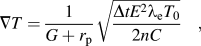 $$\nabla T = {1 \over {G + {r_{\rm{p}}}}}\sqrt {{{\Delta t{E^2}{{\rm{\lambda }}_{\rm{e}}}{T_0}} \over {2nC}}} \quad ,$$
where G is the grain size, r p is the pore radius, C is the specific heat capacity, T 0 is the temperature from which sintering is assumed to start (873 K, in this case), E is the electric field (V/m), λe is the electrical conductivity, Δt is the total (ON + OFF) pulse sequence duration, and n is the number of pulses required to reach the desired temperature. In our experiments, we used a pulse ON/OFF ratio of 12/2 which corresponds to 39.6 ms ON time and 6.6 ms OFF time. The ON pulse comprises twelve 3.3 ms pulses. Other approximate values were also plugged in: G ≈ 100 nm, r p ≈ 50 nm, Δt = 46.2 ms, n = 120220, E ≈ 1000 V/m. The values of C and λe were obtained from the literature: C 1300K ≈ 0.0175 J/K/m3.Reference Andon, Martin, Mills and Jenkins30 For a sample with residual porosity P, the heat capacity is given by C = (1 − P)C 1300K.Reference Olevsky and Froyen29 Data on the electrical resistivity of WC at high temperatures was largely unavailable. Therefore, with a knowledge of the room temperature resistivity of WC (ρ300K ≈ 20 μΩ m) and the temperature coefficient of resistivity α ≈ 4500/K,Reference Grebenkina and Denbnovetskaya31 a linear approximation was applied from 300 K to the temperature of interest (1300 K) using the relation ρ = ρ300K (1 + α ΔT). Although strictly, this might be in error, a variation of one order of magnitude in the final result may be expected owing to this approximation. The electrical conductivity (λe = 1/ρ) of a sample with residual porosity, P was calculated as λe(P,T) = λe(0,T) [(1 − P)/(1 + 2P)].Reference Olevsky and Froyen29 Using these values, ∇T ≈ 60 × 106 K/m.