I. INTRODUCTION
Silicon nanowires (SiNWs) have attracted considerable interest for a variety of applications including field-effect transistors,Reference Cui, Zhong, Wang, Wang and Lieber1 thin-film transistors,Reference Duan, Niu, Sahi, Chen, Wallace Parce, Empedocles and Goldman2 and chemical and biological sensors.Reference Cui, Wei, Park and Lieber3 For optimal device performance there is a need for low resistivity, thermally stable contacts to the nanowires. Currently, NiSi is commonly used as the contact to complementary metal–oxide semiconductor (CMOS) devices because of its low resistivity and relatively low consumption of Si compared to other attractive metal silicide phases.Reference Lavoie, d’Heurle, Detavernier and Cabral4 Current and future CMOS device designs including fin field-effect transistors are geometrically very similar to nanowire devices. Therefore, the formation of Ni silicides in contact to SiNWs is of technological interest both for continued scaling of CMOS technology and for the many potential applications of Si nanowire devices.
To date, there have been a number of studies on the reaction of Ni with SiNWs; however, widely varying results have been obtained.Reference Lu, Tu, Wu, Chen, Yoo and Myung5–Reference Dellas, Liu, Eichfeld, Eichfeld, Mayer and Mohney12 In some of these studies, the Ni silicide phase formed has not been conclusively identified. In others, different Ni silicide reaction products have been identified, including Ni31Si12,Reference Lin, Chen, Xu and Huang8 δ-Ni2Si,Reference Lin, Chen, Xu and Huang8, Reference Zhang, Lu, Hellstrom, Ostling and Zhang11 θ-Ni2Si,Reference Zhang, Lu, Hellstrom, Ostling and Zhang11, Reference Dellas, Liu, Eichfeld, Eichfeld, Mayer and Mohney12 Ni3Si2,Reference Zhang, Lu, Hellstrom, Ostling and Zhang11 NiSi,Reference Lu, Tu, Wu, Chen, Yoo and Myung5–Reference Chou, Wu, Chen and Tu7, Reference Wu, Xiang, Yang, Lu and Lieber10–Reference Dellas, Liu, Eichfeld, Eichfeld, Mayer and Mohney12 and NiSi2.Reference Lin, Chen, Xu and Huang8, Reference Weber, Geelhaar, Unger, Cheze, Kreupl, Riechert and Lugli9, Reference Dellas, Liu, Eichfeld, Eichfeld, Mayer and Mohney12 In studies by Tu and coworkers,Reference Lu, Tu, Wu, Chen, Yoo and Myung5–Reference Chou, Wu, Chen and Tu7 the point contact reaction between NiNWs and SiNWs with [111] growth directions has been observed by in-situ heating transmission electron microscope (TEM). Interestingly, they observed NiSi formation not at the point of contact between the NiNW and SiNW, but at the ends of the SiNW. The NiSi segment was found to grow linearly with time with activation energy of 1.25 eV/atom indicating that the growth is limited by an interfacial reaction. Katsman et al.Reference Katsman, Yaish, Rabkin and Beregovsky13 theoretically considered the formation of axial Ni silicide segments and concluded that growth was limited by surface diffusion with a parabolic time dependence or by diffusion across the silicide/Si interface with a linear time dependence.
Unfortunately, a strict comparison between results obtained in these previous studies is difficult because of the subtle, but important, differences between each of the studies. For instance, growth directions of the SiNWs differ between the studies and this difference affects the phase formation sequence; we believe that this difference is due to the increased role of interfacial energy minimization in the formation of nanowire silicide segments. Additionally, the heating rates during annealing by in-situ TEM are much slower than those used in rapid thermal annealing (RTA) furnaces and could also affect the reaction products.
II. EXPERIMENTAL
Samples were fabricated by a method described previously,Reference Dellas, Liu, Eichfeld, Eichfeld, Mayer and Mohney12 with the lone exception being that the backside of the wafer was not etched away because of the use of field-emission scanning electron microscopy (FESEM; Leo 1530) rather than TEM to measure the silicide lengths. The SiNWs with [112] growth directions were grown by the vapor–liquid–solid (VLS) method from oxidized Si substrates to a length of 20 μm using SiH4 as a Si precursor gas, and SiNWs with [111] growth directions were also grown epitaxially by the VLS technique to lengths of 20 μm from [111] Si wafers using SiCl4 as the Si precursor gas, as determined by TEM using a JEOL JEM-2010F (JEOL, Tokyo, Japan) with a field-emission source. The average diameters of the SiNWs with [112] and [111] growth directions were 60 and 63 nm, respectively, with diameters ranging from as low as 50 to as high as 75 nm for both types of SiNWs. Samples were annealed ex situ in a RTA furnace (Heat Pulse 610, AG Associates, Fremont, CA) purged with Ar (purity of 99.999%) at temperatures of 400, 450, 500, and 550 °C for times of 0, 2, 4, 8, and 12 min, respectively. Single samples were annealed at each time and temperature, and the Ni silicide length of at least 10 segments was measured under each annealing condition. The data reflect the average growth length of Ni silicide for each annealing condition. The data point of 0 min consisted of a ramp up to the annealing temperature followed immediately by cooling to determine the amount of Ni silicide growth during ramp up to the annealing temperature and during cool down for each annealing condition.
III. RESULTS AND DISCUSSION
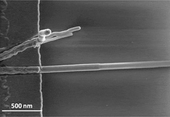
Silicide lengths were studied as a function of temperature and time to determine the kinetics and identify rate-limiting steps in the formation of Ni silicides, as well as to learn about differences when SiNWs with [111] and [112] growth directions are used. An FESEM (Leo 1530) was used to measure the silicide lengths, and the growth directions were verified a second time by observing the facets on the SiNW segments. SiNWs with [111] growth directions displayed a hexagonal cross section, and SiNWs with a [112] growth direction displayed a rectangular cross section. Figure 1 shows an FESEM image of a nanowire annealed at 450 °C with an 80-nm-thick contact pad, and the length of the silicide segment is obvious from the contrast.
Field-emission scanning electron microscopy image of a [111] silicon nanowire (SiNW) after reaction with a Ni pad at 450 °C for 2 min. The cross sections of [111] SiNWs are hexagonal, and the surface facets can be seen from the plan-view scanning electron microscopy image. The surface morphology of the SiNW segment was used to verify the identity of [111] and [112] SiNWs.

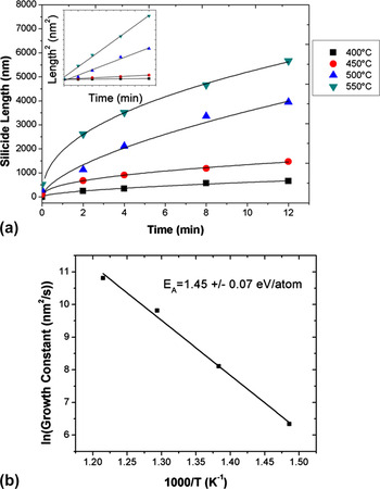
A plot of the silicide length as a function of time for different temperatures for the [112] SiNWs is shown in Fig. 2(a). It is clear that the time dependence is not linear but is parabolic in nature, as indicated by the inset in Fig. 2(a), where a plot of the square of Ni silicide length versus time for the [112] SiNWs is a straight line. This parabolic time dependence is indicative of a diffusion-limited reaction. The growing silicide phase was identified by the earlier TEM study as θ-Ni2Si.Reference Dellas, Liu, Eichfeld, Eichfeld, Mayer and Mohney12 The θ-Ni2Si phase is a high-temperature phase in the Ni–Si system and usually not encountered in thin-film reactions; therefore, there is limited information about kinetic parameters for the growth of this phase in thin films, such as the activation energy of diffusion through the lattice or grain boundaries. However, for the low-temperature orthorhombic δ-Ni2Si phase, many studies have been performed analyzing the kinetics of growth. The activation energy for the growth of this phase is typically 1.3–1.5 eV/atom, and growth of δ-Ni2Si is limited by grain boundary diffusion of Ni through the growing δ-Ni2Si layer, as determined by radioactive tracer studies.Reference Ciccariello, Poize and Gas14 From the plot of the natural logarithm of the θ-Ni2Si growth rate constant versus 1000/kT [Fig. 2(b)], where k is Boltzmann’s constant and T is temperature, we extract an activation energy of 1.45 ± 0.07 eV/atom. Furthermore, this value compares favorably with the activation energy observed (1.4 eV/atom) for lateral diffusion couples forming δ-Ni2SiReference Zheng, Hung, Mayer, Majni and Ottaviani15. The activation energy we have extracted (1.45 eV/atom) falls well within the range of activation energies identified for growth (1.3–1.5 eV/atom) of the low-temperature δ-Ni2Si phase. A major difference between our nanowire geometry and the thin-film geometry is that for the thin-film case, a polycrystalline δ-Ni2Si layer can form with grain boundaries acting as fast pathways for diffusion. For the single crystal θ-Ni2Si nanowire segment, there are no grain boundaries; however, the SiO2/silicide interface may act as a fast pathway for diffusion. Therefore, the rate-limiting mechanism for the formation of the θ-Ni2Si segment is likely diffusion of Ni along the θ-Ni2Si/SiO2 interface. Note that the SiNW surface or the θ-Ni2Si surface itself is not exposed and is always surrounded by SiO2. Additionally, we observe similar lengths of θ-Ni2Si segment for intentionally oxidized and as-grown SiNWs. We believe that Ni is the dominant diffusing species in the axial formation of the Ni silicide segment since Kirkendall-like voids begin to form in the Ni pad surrounding the SiNW for severe annealing conditions such as 550 °C for 12 min.
(a) Silicide length versus time for the [112] SiNWs. The inset shows length squared versus time, demonstrating parabolic growth kinetics. (b) An Arrhenius plot revealing an activation energy for θ-Ni2Si formation of 1.45 ± 0.07 eV/atom. Error bars calculated as the standard deviation from 10 or more measurements, with the average being the data point. Note: error bars smaller than symbols for lower temperature data.

There is only a small range of diameters used in this work, and we find no more than a 10% variation in silicide length among different nanowires treated identically. However, a model by Katsman et al.Reference Katsman, Yaish, Rabkin and Beregovsky13 indicates that for the case of diffusion along the periphery of the nanowire as the rate-limiting step, silicide length will scale with  , where R is the nanowire radius. Considering this dependence, we extract an activation energy of 1.48 ± 0.15 eV, which is very nearly the same as we found without accounting for the SiNW diameter. The similarities in activation energy indicate that the average diameters used for each data point in the kinetic analysis are in a tight enough range that our results are not greatly affected by the SiNW diameter.
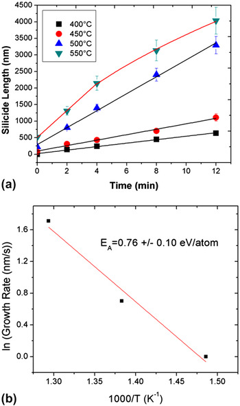
In the case of the NiSi2 growth from [111] SiNWs, the time dependence of the growth of the NiSi2 nanowire segment is linear [Fig. 3(a)] at 400, 450, and 500 °C. The linear time dependence is determined by the slope of a plot of the natural log of Ni silicide length versus the natural log of time, where a slope of 0.5 would indicate parabolic kinetics and 1.0 would indicate linear kinetics. For the annealing temperatures of 400, 450, and 500 °C, the slope of this plot is between 0.92 and 0.93 indicating that the Ni silicide growth is well represented by a linear time dependence. The slope of this same plot for the 550 °C annealing condition is 0.78. An intermediate time dependence can indicate that the rates of diffusion and interfacial reaction are comparable.
(a) Silicide length versus time for SiNWs with the [111] growth direction. The growth with time is linear indicating that an interfacial reaction is the rate-limiting step for formation at temperatures of 400, 450, and 500 °C. (b) Arrhenius plot used to for extraction of an activation energy for NiSi2 formation of 0.76 ± 0.10 eV. Error bars calculated as the standard deviation from 10 or more measurements, with the average being the data point. Note: error bars smaller than symbols for lower temperature data.

Linear kinetics often indicates that an interfacial reaction is the rate-limiting step, and for the [111] SiNWs, the rate-limiting step for silicide formation could be the rearrangement of atoms at the NiSi2/SiNW interface to form additional NiSi2. The activation energy extracted from the slope of the plot of the natural log of the growth rate of NiSi2 versus 1000/kT [Fig. 3(b)] is 0.76 ± 0.10 eV, calculated using data from only the 400, 450, and 500 °C annealing conditions. Alternatively, Katsman et al.Reference Katsman, Yaish, Rabkin and Beregovsky13 have suggested that linear growth kinetics of silicide nanowire segments could be due to rate-limiting radial diffusion from the nanowire periphery across the growth front. In this case, the distance from the periphery of the silicide segment to the interface remains constant as the growth of the Ni silicide segment proceeds, resulting in a dependence on time to the first power. Though we cannot distinguish between these two possibilities, we note that for the latter case, silicide length is predicted to scale with t/R 2. In normalizing the kinetic data to the square of the SiNW radius, we extract an activation energy of 0.78 ± 0.1 eV, again very similar to the value we already reported.
IV. CONCLUSIONS
In conclusion, we have identified differences in the reaction kinetics between Ni silicidation of [111] and [112] SiNWs. In the case of [111] SiNWs, the kinetics are linear with an activation energy of 0.76 ± 0.10 eV. For the case of [112] SiNWs, the kinetics are parabolic with an activation energy of 1.45 ± 0.07 eV/atom, a value significantly lower than expected for lattice diffusion, indicating that the pathway for diffusion is likely at the θ-Ni2Si/SiO2 interface of the nanowire. These results also indicate that for the integration of SiNWs into high performance devices with uniform silicide lengths, all starting SiNWs should have the same growth direction.
ACKNOWLEDGMENTS
The authors thank Prof. Long-Qing Chen for discussion and Prof. Joan Redwing for supplying SiNWs. The use of the Penn State Nanofabrication Facility [National Science Foundation (NSF), National Nanotechnology Infrastructure Network (NNIN) ECCS-0335765] is also acknowledged. The authors are grateful for financial support from NSF ECS-0609282 (to N.S. Dellas), as well as Army Research Office W911NF-09-1-0140 and the Gates Foundation (to M. Abraham).