I. INTRODUCTION
Wireless communication technology has developed rapidly in recent years. As essential elements of wireless communication system, antennas of better performance are required such as miniaturized size, dual or multi-band operation, and simple structure [Reference de Cos, Mantash, Tarot and Las-Heras1, Reference Lee, Kwon, Kang and Lee2]. Also, circularly polarized antennas are widely used in many systems instead of traditional linear polarized antenna, such as wireless local area network (WLAN), to enhance the polarization efficiency of the link budget [Reference Ghobadi and Dehmollaian3, Reference Wu, Shi, Li and Bai4]. What is more, in a single compact wireless communication system, is a multiband antenna with good polarization purity or different polarization property in different band for multiple communication standards.
Microstrip patch antenna has advantages of low profile, low cost, easy fabrication, and compatibility with integrated circuit technology [Reference Lee and Tong5]. There are many methods of designing dual or multiband antennas using patches. A dual-band patch antenna can be realized by activating TM100 and TM010 mode which shows different resonant frequency and orthogonal polarization [Reference Veysi, Kamyab and Jafargholi6]. Cutting slots on the patch or ground plane is commonly used in broadening impedance bandwidth and exciting multiple resonant frequencies [Reference Lee, Yang and Kishk7–Reference Chakraborty, Kundu, Chowdhury and Bhattacharjee10]. Fractal patches have also been proposed for multiband, broadband, and miniature antennas because the iteration of fractal geometries easily induces multi-resonance. The lowest resonant frequency decreases as the number of iteration increases [Reference Azari11–Reference Oraizi and Hedayati14]. Stacked patch technique is used in many studies to realize multiband antenna. A stacked patch antenna is constructed by one or more driving patches and parasitic patches. The working band and polarization can be tuned separately and conveniently, so many dual or triple band circularly polarized antennas are designed by this method [Reference Falade, Rehman, Yue, Chen and Parini15]. Most of the multiband antennas have the same polarization in different frequency band, but [Reference Zhou, Wang, Wang, Zong and Ma16] utilizing the special property of composite right/left handed transmission line and complimentary split-ring resonator proposed a dual-band antenna, which has a linearly polarized radiation at the lower frequency and a circularly polarized radiation at the upper frequency. However, the present designs are always complicated and different to redesign according to varied specifications. And the gain is usually decreased, while dual-band operation or different polarizations are realized by a single radiation structure.
In this paper, patch antennas with meandering slot are adopted to stimulate dual-band operation with high gain. Then, grounded metallic vias are further added. Different radiation performances are easily achieved by changing the number and position of grounded vias. In addition, the existence of vias will also improve the impedance matching. The simulated and measured results show good agreement. Four samples are provided to illustrate the easy design of antennas with varied working frequency band and polarization.
II. ANTENNA STRUCTURE ANALYSIS
A) Dual-band operation realized by adding meandering slot to a patch antenna
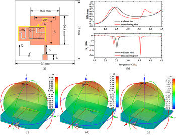
The proposed antennas are optimized by the Finite Integration Technique of computer simulation technology microwave studio. The geometry of microstrip patch antenna with meandering slot is shown in Fig. 1(a). The antenna is fed by a 50 Ω microstrip line cascaded with a high impedance line for impedance matching. The substrate has thickness of h = 2 mm and permittivity ε r = 2.5 with tanδ = 0.002. The ground plane size is 75 × 75 mm2 and the patch size is 36.8 × 36.8 mm2. The width of slot is 0.15 mm. The relative reflection coefficient (S 11) and three-dimensional (3D) radiation pattern at two working frequencies are presented in Figs 1(b)–1(d), respectively. By contrasting, the simulated results of a traditional patch antenna without meandering slot are also presented with its reflection coefficient in Fig. 1(b) and 3D radiation pattern at one working frequency in Fig. 1(e). Figure 1(b) gives the comparison of radiation efficiency about the patch with and without meandering slot. For the first resonant frequency, the radiation efficiency is almost the same at the resonant frequency. In the meandering slot case, the radiation efficiency for the second resonant frequency is slightly lower than the first frequency.
Microstrip patch antennas: (a) geometry structure of patch antenna with meandering slot (Note: l 1 = 6.9 mm, l 2 = 12 mm, l 3 = 31.4 mm, l 4 = 26 mm, g = 2.5 mm, and d = 1 mm), (b) simulated S 11 and radiation efficiency of patch antennas with and without meandering slot, (c) 3D radiation pattern of patch antenna with meandering slot at 2.373 GHz, (d) 3D radiation pattern of patch antenna with meandering slot at 3.51 GHz, and (e) 3D radiation pattern of patch antenna without meandering slot at 2.51 GHz.

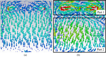
The dual-band operation is observed by adding a slot near the radiation ends. The working frequency of 2.51 GHz in the traditional patch antenna goes down to 2.37 GHz when a slot is added, because the route of surface current becomes longer. This is clearly proved by the surface current distributions illustrated in Fig. 2(a), where a fundamental radiation mode of TM100 mode is induced at 2.37 GHz. A TM200 mode is observed at 3.51 GHz which is obviously induced by the interference of the meandering slot. The magnitude of current is very small near the slot, so it has little affection to the TM100 mode except the working frequency. But to TM200 mode, as shown in Fig. 2(b), the resonant slot divides the surface current distribution into two parts. In part 1, the current has opposite direction, so the radiation of this part is mostly cancelled. Then the main radiation is decided by part 2, which occupies most area of the patch. The maximum gain at 3.51 GHz is 5.97 dB which is only 0.17 dB less than the traditional patch antenna without meandering slot.
The surface current of (a) TM100 mode at 2.37 GHz, and (b) TM200 mode at 3.51 GHz.

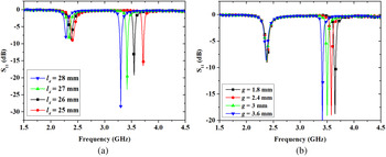
The length and shape of the slot will affect the resonant frequency of TM200 mode for the changing of current route in part 1. Figure 3 shows the effect of changing the length l 4 and width g of the meandering slot. When the l 4 is increased, the two frequencies are decreased and for both, the current goes along a longer way. Increasing g results in reducing the second frequency and the first frequency do not change.
The S 11 versus different length of (a) l 4 and (b) g.

B) Varied radiation performance realized by tuning the number and position of grounded vias
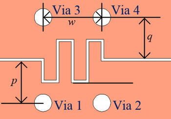
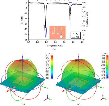
The possible position of vias is shown in Fig. 4. When only Via 1 or Via 2 exists, the TM100 mode and TM200 mode can be excited at the same time. Dual-band working states are maintained. If the via is placed at the left (with Via 1) or right side (with Via 2) of the center line, the polarization of the lower frequency will change. For example, in terms of the situation with Via 2 in Fig. 4, to TM100 mode, the via equals to an inductance connected to the U strip on the right side. The different current route of right and left side changes the phase of surface current. So the antenna has a right-handed circular polarization at lower band of TM100 mode. To TM200 mode, the via also equals to an inductance. But influenced by the next resonant area (part 2 in Fig. 2), the inductance is negative which shortens the resonant length on U strip and results in an increased working frequency. If the via is placed at the left side, the analysis is similar. The only difference is that a right-handed circular polarization of the antenna with Via 2 is changed to a left-handed circular polarization of the antenna with Via 1. Figure 5(a) shows the simulated S 11 and axial ratio (AR). Figures 5(b) and 5(c) shows the 3D radiation patterns of the two central frequencies. The simulated gain is 6.56 dB of right hand polarization at 2.462 GHz and 6.495 dB of linear polarization at 3.828 GHz, respectively. For the improved impedance matching, the gain is slightly higher than that in the situation only with meandering slot.
Geometry structure of the possible position of four vias. (Note: p = 2.4 mm, w = 3.34 mm, and q = 2.35 mm).

The simulated S 11 and AR in (a), the 3D radiation pattern of the right hand polarization of 2.462 GHz in (b), and linear polarization of 3.828 GHz in (c).

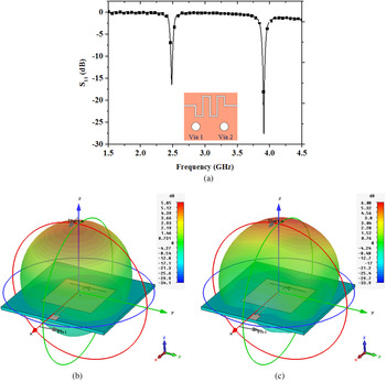
If Via 1 and Via 2 both exist, and they are symmetrical with the original via along the center line, the circular polarization of lower frequency becomes linear. In this situation, the two U strips add inductance on the ends. Therefore, the phase shift of TM100 mode current cancels out. But the negative inductance effect still exists on the TM200 mode. So the frequencies of two bands are the same as the previous antenna, but the polarizations are both linear. Compared with the antenna without via, antenna with vias has a better impedance matching at the lower band, which is because the equivalent inductance has compensated to the input impedance of lower band, but has little effect on the higher band. The simulated S 11 of antenna with Via 1 and Via 2 is shown in Fig. 6(a). Figures 6(b) and 6(c) shows the 3D radiation pattern of the two central frequencies. The simulated gain is 5.851 and 6.082 dB, respectively.
The simulated S 11 in (a), the 3D radiation pattern of 2.49 GHz in (b), and of 3.927 GHz in (c).

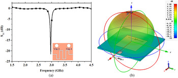
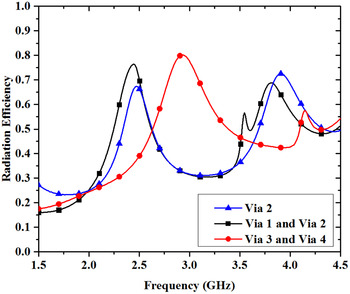
If the antenna has Via 3 and Via 4, the TM100 mode resonant seriously presents mismatching, so there is only TM200 mode working. In this situation, the antenna becomes a single band and linearly polarization antenna. Figure 7 shows its S 11 and 3D radiation pattern of the central frequency. The simulated gain is 7.027 dB. From the simulated gain and radiation patterns, we can see that adding vias to the meandering slot patch antenna has little change of the shape of radiation pattern. For the optimizing of the impedance matching, the realized gain is still near to the original antenna in both frequencies. The radiation efficiency of only Via 2, Via 1 and Via 2, Via 3 and Via 4 is shown in Fig. 8. The antenna with Via 3 and Via 4 has the highest radiation efficiency among the three antennas which approaches the antenna without via. The antenna with Via 1 and Via 2 has higher radiation efficiency than the antenna with only Via 2 at the first resonant frequency, while the only Via 2 antenna has higher efficiency at the second resonant frequency.
The simulated S 11 in (a), and 3D radiation pattern of 2.973 GHz in (b).

The radiation efficiency of only Via 2, Via 1 and Via 2, Via 3 and Via 4.

III. FABRICATION AND MEASUREMENT
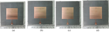
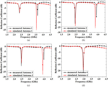
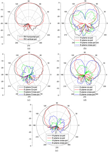
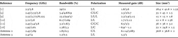
Four samples are finally fabricated and measured. To express conveniently, the antenna without slot is named as Antenna 1, the antenna with only Via 2 is named as Antenna 2, the antenna with Via 1 and Via 2 is named as Antenna 3, the antenna with Via 3 and Via 4 is named as Antenna 4. The photographs and their reflection coefficient are illustrated in Figs 9 and 10, respectively. The simulated AR of Antenna 2 at 2.448 GHz is 1.15 dB and measured result is 0.86 dB which indicates a good circular polarization. A reasonable agreement is observed between the measured and simulated results. The radiation pattern has been measured in an anechoic chamber at the center frequencies of 2.45 and 3.89 GHz for Antenna 2, 2.47 and 4 GHz for Antenna 3, 2.95 GHz for Antenna 4. The relative results are shown in Fig. 11. The measured gain for Antenna 2 is 6.114 dB (right hand polarization gain) at 2.45 GHz and 5.683 dB at 3.89 GHz (linear polarization gain), for Antenna 3 is 6.314 dB at 2.47 GHz and 5.04 dB at 4 GHz, for Antenna 4 is 5.315 dB at 2.95 GHz. The cross-polarization level approaches −20 dB at the maximum radiating direction of the three antennas. Table 1 illustrates the comparison of antennas in this paper and in references. As we can see, the antennas in this paper show higher gain and more choices in polarization. Although the bandwidth is relatively small, our antennas have much simplified structures and also have possibility of reconfigurable design.
Photographs of (a) Antenna 1 with meandering slot, (b) Antenna 2 with meandering slot and Via 2, (c) Antenna 3 with meandering slot, Via 1 and Via 2, and (d) Antenna 4 with meandering slot, Via 3 and Via 4.

Relative reflection coefficients of (a) Antenna 1 with meandering slot, (b) Antenna 2 with meandering slot and Via 2, (c) Antenna 3 with meandering slot, Via 1 and Via 2, and (d) Antenna 4 with meandering slot, Via 3 and Via 4.

Measured radiation patterns of (a and b) Antenna 2 at 2.45 and 3.89 GHz, respectively, (c and d) Antenna 3 at 2.47 and 4 GHz, respectively, and (e) Antenna 4 at 2.95 GHz.

Comparison of references and proposed antennas.

Note: L, Linear polarization; C, Circular polarization.
IV. CONCLUSION
A novel design of dual-band circular- and linear-polarization antenna has been proposed. The meandering slot induces dual-band operation. The introducing of vias brings different frequency and polarization properties, which allows diversity design. The antenna shows good performance at cross-polarization and gain. This method can be used not only in reconfigurable antennas, but also in multiband patch antenna with different polarization.
ACKNOWLEDGEMENTS
This work was supported in part by the Program for New Century Excellent Talents in University (grant NECT-13-0095), in part by the State Key Laboratory of CEMEE Foundation (grant CEMEE2015K0201B), in part by the Scientific Research Foundation for the Returned Overseas Chinese Scholars, State Education Ministry.
 Jin Zhang was born in Anshun, Guizhou Province, China, in October 1989. She received her B.Sc. degree in Electromagnetic fields and Microwave technology at University of Electronic Science and Technology of China (UESTC) in 2008 and is currently working towards Ph.D. degree in Electromagnetic fields and Microwave technology at UESTC. Her research interests include antenna design and theory.
 Xianqi Lin was born in Zhejiang Province, China, on July 9, 1980. He received his B.S. degree in Electronic Engineering from University of Electronic Science and Technology of China (UESTC), Chengdu, China, in 2003, and Ph.D. degree in Electromagnetic and Microwave technology from Southeast University, Nanjing, China, in 2008. He joined the Department of Microwave Engineering at UESTC in August 2008, and has become an Associate Professor and a doctoral supervisor since July 2009 and December 2011, respectively. From September 2011 to September 2012, he was a post-doctoral researcher in the Department of Electromagnetic Engineering at the Royal Institute of Technology (KTH), Stockholm, Sweden. He has authored over 10 patents, over 40 scientific journal papers, and has presented over 20 conference papers. His research interests include microwave/millimeter wave circuits, metamaterials and antennas.
 Jiawei Yu was born in Chengdu, Sichuan Province, China, in March 1991. He received his B.Sc. degree in Electromagnetic fields and Microwave technology at University of Electronic Science and Technology of China (UESTC) in 2008 and is currently working towards Ph.D. degree in Electromagnetic fields and Microwave technology at UESTC. His research interests include microwave filter and antennas.
 Liying Nie was born in LinYi, Shandong Province, China, in March 1991. She received her B.E. degree in Antennas and Radio Propagation from University of Electronic Science and Technology of China (UESTC), Chengdu, Sichaun, China, in 2014, and is currently working towards the M.E. degree in Electromagnetic fields and Microwave technology at UESTC. Her research interests include antenna and filter design.