I. INTRODUCTION
In recent years, research into using carbon nanomaterials as an electronic conducting material has grown due to the exceptional theoretical properties exhibited by these nanomaterials. Reference Iijima1,Reference Iijima and Ichihashi2 Concurrently, the field of paper electronics has soared in popularity due to the low-cost and widespread availability of paper. Reference Tobjork and Osterbacka3 Combining paper substrates with electronic nanomaterials can be used in a variety of applications including energy storage, Reference Hu, Choi, Yang, Jeong, La Mantia, Cui and Cui4–Reference Weng, Su, Wang, Li, Du and Cheng6 sensors, Reference Nery and Kubota7 field-effect transistors, Reference Lyth and Silva8 and solar cells Reference Barr, Rowehl, Lunt, Xu, Wang, Boyce, Im, Bulovic and Gleason9 among others. Reference Tobjork and Osterbacka3,Reference Zheng, Cui, Karabulut, Wagberg, Zhu and Hu10 Because of the increasing popularity in this field, it is important to gain a complete understanding of the interactions between the active nanomaterial and the paper backbone and how these interactions impact the properties of these composites.
Because of the porous nature of paper, deposition of the carbon nanomaterial can occur both on top of and within the paper structure. Most studies have focused on deposition of the nanoparticulate materials on top of the paper, Reference Hu, Choi, Yang, Jeong, La Mantia, Cui and Cui4,Reference Barr, Rowehl, Lunt, Xu, Wang, Boyce, Im, Bulovic and Gleason9–Reference Fortunato, Correia, Barquinha, Pereira, Gonçalves and Martins11 whereas a few others have utilized layer-by-layer assembly Reference Peng, Thio and Gerhardt12–Reference Gittleson, Kohn, Li and Taylor14 or Meyer-rod coating. Reference Hu, Choi, Yang, Jeong, La Mantia, Cui and Cui4,Reference Huang, Chen, Peng and Gerhardt15 Yet others have attempted to make 3D-interconnected cellulose-based composites containing a variety of graphitic fillers including graphene, Reference Weng, Su, Wang, Li, Du and Cheng6 carbon nanotubes, Reference Tanaka, Sano, Imai and Akiyama16 carbon black (CB), Reference Hong, Park and Shim17 and graphene oxide Reference Han, Yan, Chen, Li and Bangal18 to name a few. Among these, one of the more impressive is the effect of the filler concentration of graphene nanosheets (GNSs) in forming a conductive composite. Reference Weng, Su, Wang, Li, Du and Cheng6 It was found that with only 7.5 wt% of GNS, uniform deposition via vacuum filtration of the sheets on the paper fibers led to a resistance of 6 Ω, and the paper–GNS composite could withstand a stress of 8.67 MPa with 3% elongation. Reference Weng, Su, Wang, Li, Du and Cheng6
Recently, work has been done to elucidate what effect different deposition parameters have on the electrical properties of multiwalled carbon nanotube (MWNT) films deposited on paper substrates using dropcasting methods. Variables explored include dispersion concentration and number of layers, Reference Muhlbauer and Gerhardt19 as well as drying technique. Reference Muhlbauer, Joshi and Gerhardt20,Reference Muhlbauer and Gerhardt21 It was shown that when the pore size of the paper substrate is comparable to the length of the carbon nanotubes, the drying method has a minimal impact on the structure and electrical properties of the film because film formation is occurring mostly at the surface of the paper. When the pore size of the paper is much larger than the length of the tubes (>25x), drying technique results in a large variation in microstructure and electrical properties. Reference Muhlbauer, Joshi and Gerhardt20,Reference Muhlbauer and Gerhardt21
The main goal of this paper is to provide further insight into the structure–property relationships of paper-based carbon nanomaterial layered composites, by studying composites made up of 1–20 layers of a variety of carbon nanomaterials deposited on the same type of paper substrate with a small pore size of 1 μm. The smallest pore size was used to focus on the effect of the filler shape and size. Fillers evaluated were graphite flakes, single-walled carbon nanotubes (SWNTs), short MWNTs, and CB. It is important to note that for all specimens tested, the same fabrication technique, paper backbone, and dispersion parameters were used to allow for a systematic study of the effect of the number of layers of the different nanocarbons used. Scanning electron microscopy (SEM) images revealed their arrangement on top of the paper substrates. The electrical and thermal properties were characterized and compared to the structure of each paper–carbon nanomaterial composite system.
II. EXPERIMENTAL METHODS
A. Chemicals and materials
Four different carbon nanomaterials of various shapes and sizes were used in this experiment: MWNTs, SWNTs, CB, and graphite flakes. MWNTs were obtained from cheaptubes.com with the following specifications: 0.5–2.0 µm in length, 8–15 nm in diameter, >95 wt% purity with <1.5 wt% ash. SWNTs were fabricated using a laser growth method at Oak Ridge National Lab (Knoxville, TN) and have an average diameter of 1.5 nm with a yield of 1/3 metallic and 2/3 semiconducting SWNTs. Reference Garrett22 Grade 3775 surface enhanced natural flake graphite (5–10 µm length, ∼100 nm thickness, >98 wt% purity) was purchased from Asbury Carbons (Asbury, NJ), whereas CDX-975 grade CB was obtained from Columbian Chemicals Company (Marietta, GA). The CB used has a nominal mean particle size of 21 nm, although it does undergo some agglomeration. Reference Ou, Gupta, Parker and Gerhardt23 Sodium dodecylbenzenesulfonate (SDBS) was purchased from Sigma-Aldrich (St. Louis, MO). Cellulose-based qualitative filter papers of 1-µm pore size were obtained from VWR.com.
B. Nanomaterial dispersion and composite film preparation
Dispersions containing 1 mg/mL of each carbon material, 10 mg/mL SDBS, and DI water were prepared using a modified method from Refs. Reference Huang, Chen, Peng and Gerhardt15 and Reference Muhlbauer, Joshi and Gerhardt20. First, the carbon material was added to DI water and ultrasonicated for 10 min. Next, the SDBS surfactant was added slowly to the carbon/water mixture over another 10 min time interval while undergoing ultrasonication. Last, once the entirety of the surfactant was added, the mixture was sonicated for 60 min and then magnetically mixed for 12 h to ensure complete dispersion of the carbon material.
Because the deposition technique used can result in different distribution of the dispersed material both on the surface and within the bulk of the paper substrate, only the vacuum filtration technique Reference de Heer, Bacsa, Chatelain, Gerfin, Humphrey-Baker, Forro and Ugarte24 was used to form the layered paper composite materials studied in this paper. For each layer (from 1 to 20), 50 µL of the carbon material dispersion was dropcasted onto the paper substrate backbone and filtered. Once each layer dried, the next layer was deposited using the same technique until the required number of layers was obtained.
C. Characterization techniques
The electrical properties of the composite films were measured for both the surface (in-plane) and across the thickness (thru-plane) using impedance spectroscopy, an alternating current (AC)-based electrical characterization technique. Reference Peng, Thio and Gerhardt12,Reference Gerhardt25,Reference Gerhardt, Bassani, Liedl and Wyder26 Although direct current (DC) electrical techniques are a popular method to obtain electrical properties of materials, DC techniques only allow for the determination of the overall resistance of the material and, even though they are very useful for giving an indication of the electrical response, a lot of detailed information regarding the structure of the materials being measured is lost. In contrast, AC electrical characterization techniques are more sensitive to the various electrical processes present in the material, allowing for the separation of the resistance due to each process from the overall resistance of the material. Reference Muhlbauer, Joshi and Gerhardt20,Reference Gerhardt25–Reference Garrett, Ivanov, Gerhardt, Puretsky and Geohegan28
Impedance spectroscopy was carried out using two equipment setups: Solartron 1260 alone for the more conducting samples and Solartron 1296 connected to the Solartron 1260 for the more insulating samples (Hampshire, U.K.). For the in-plane measurements, a two-probe measurement technique was used to determine the surface behavior, and the measurements were carried out by scanning the frequencies from 21 MHz to 0.01 Hz using an AC voltage of 0.1 V for the MWNT and SWNT samples to ensure completion of the impedance response. The frequency maximum was 10 MHz for the insulating sample arrangement. For the thru-plane measurements, the samples were placed in a parallel plate arrangement and measured using the high resistance impedance setup with an AC voltage of 4 V. Nyquist plots (complex Z″ versus Z′ graphs) are presented for each sample with frequency increasing toward the lowest x-intercept value.
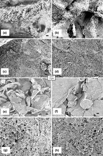
In-lens SEM images of the composite surfaces were taken using a Zeiss SEM. Ultra60 (Oberkochen, Germany) at 1–2 kV. Figure 1 shows the film surfaces for CB (1a and 1b), MWNT (1c and 1d), graphite flakes (1e and 1f), and SWNT (1g and 1h). Images on the left are for 4-layered films, whereas those on the right are for the 20-layered samples. In all cases, the scale bar reads 2 µm.
SEM micrographs of the composite surfaces for CB (1a and 1b), MWNT (1c and 1d), graphite (1e and 1f), and SWNT (1g and 1h) and paper composites. Images on the left are for 4-layered films, whereas those on the right are for 20-layered samples. The scale bar reads 2 µm.

Thermal characterization of the powders, paper filters, dispersions, and paper–carbon nanomaterial composites was done using a TA Instruments SDT Simultaneous Q600 Differential Scanning Calorimetry/Thermogravimetric Analysis (DSC/TGA; New Castle, DE). Samples were scanned from room temperature to 900 °C (600 °C maximum for the paper-only sample) in air using a 20 °C/min heating rate. At maximum temperature, the samples were held isothermally for 5 min before the machine was cooled. Weight (%) and heat flow (W/g) versus temperatures graphs were analyzed for weight loss events.
III. RESULTS AND DISCUSSION
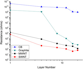
Figure 2 displays the low frequency resistance for the in-plane measurements for all of the films fabricated and characterized as a function of the number of layers deposited (this is equivalent to DC resistance as described before Reference Muhlbauer, Joshi and Gerhardt20 ). It is clear that the films made from the CB dispersion never achieve a fully interconnected state as they remain highly resistive even after 20 deposition layers. The films made from the graphite flakes are somewhat more conductive and do show the appearance of a percolative transition. For the MWNT and SWNT films, they already appear percolated as their resistance is many orders of magnitude lower than that for the CB and the graphite flakes and their resistance value. This response is in agreement with the SEM micrographs displayed in Fig. 1, which showed high magnification images of the composite films that consist of 4 layers and 20 layers for the CB, MWNT, graphite flakes, and SWNT, respectively.
Comparison of the low frequency AC resistance for all nanomaterial–paper composite films fabricated and measured.

However, the impedance spectroscopy data obtained for the frequency range of megahertz to millihertz contain a lot more information than are contained in Fig. 2. Figures 3–6 display the complex impedance graphs of all films characterized. Equivalent circuit fitting was done for all impedance data using ZView Software, and assignment of the equivalent circuit elements due to the different microstructural components of the composites was done using a combination of SEM and thermal property characterization as will be described in more detail below.
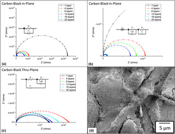
CB and paper composite impedance curves for the in-plane behavior of (a) 1 deposited layer and (b) 4–20 deposited layers of CB. (c) The impedance curves of the thru-plane for 1–20 deposited layers of CB. The equivalent circuit used to fit the impedance spectra is available within each figure. (d) A low-magnification SEM image of the surface of the film with 20-CB-deposited layers. Magnification marker = 5 μm.

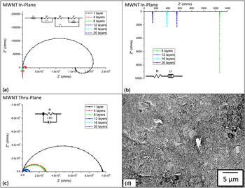
MWNT and paper composite impedance curves for the in-plane behavior of (a) 1 and 4 deposited layers and (b) 8–20 deposited layers. (c) The thru-plane impedance behavior for the MWNT and paper materials. The equivalent circuit used to fit the impedance spectra is available within each figure. (d) A low-magnification SEM image of the surface of the film with 20-MWNT-deposited layers. Magnification marker = 5 μm.

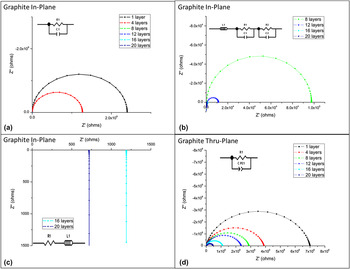
Graphite and paper composite impedance curves for the in-plane behavior of (a) 1 and 4 deposited layers; (b) 8 and 12 deposited layers; and (c) 16 and 20 deposited layers of graphite. (d) The impedance behavior for the thru-plane for the 1–20 deposited layers of graphite. The equivalent circuit used to fit the impedance spectra is available within each figure.

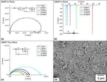
SWNT and paper composite impedance curves for the in-plane behavior of (a) 1 deposited layer and (b) 4–20 deposited layers of SWNTs. (c) The impedance behavior of the thru-plane measurements for 1–20 deposited layers of SWNTs. The equivalent circuit used to fit the impedance spectra is available within each figure. (d) A low-magnification SEM image of the surface of the film with 20-SWNT-deposited layers. Magnification marker = 5 μm.

A. Electrical properties of CB and paper composites
Figure 3 shows the impedance behavior for the in-plane measurements [Figs. 3(a) and 3(b)] and the thru-plane measurements [Fig. 3(c)] for the CB and paper composites for the 1–20 deposited CB layer samples together with an image showing that the CB never does fill all of the space even at 20 layers [Fig. 3(d)]. Equivalent circuit analysis revealed that for the in-plane, these composites show two different electrical responses as loading (number of deposited layers) of the CB increases. In Fig. 3(a), the 1 deposited layer of CB sample behavior is presented and fitted with a single parallel R–C circuit (R = 4.32 × 10¹⁰ ± 2.4 × 10⁹ Ω and C = 2.1 × 10⁻¹² ± 3.9 × 10⁻¹³ F). Such a large resistance indicates that CB does not form a fully interconnected network and that the paper fibers are dominating the surface electrical properties of this composite. At 1 layer, most of the deposited CB is filtered through the paper given that the particle size is so small (21 nm) compared to the paper pore size, even if the particles are agglomerated.
At four layers and beyond [Fig. 3(b)], the complex impedance data have a slightly different shape, even though the total low frequency resistance shown in Fig. 2 does not appear to show a change. Reference Gerhardt25 The graph in Fig. 3(b) is fitted by a different equivalent circuit containing a high frequency inductor, L 1, a parallel R 1–CPE1, and a parallel R 2–C 2, the values of which are presented in Table I. L 1 is an instrument artifact which occurs at very high frequencies for certain systems when another electronic process is not dominating at those frequencies. R 1 decreases 2 orders of magnitude with increased loading, whereas R 2 decreases but remains similar for all composites. Considering the images in Figs. 1(a) and 1(b), it is likely that the R 1–CPE1 corresponds to the pockets of CB particles which coat regions of the surface while the R 2–C 2 part of the circuit corresponds to the paper fibers as even at 20 layers [Figs. 1(b) and 3(d)], the surface still shows regions of uncoated paper fibers.
Equivalent circuit values for the circuit in Fig. 3(b) corresponding to 4–20 deposited layers of CB for impedance behavior measured on the composite surface.

The CPE, or constant phase element, is generally used to describe a distribution of relaxation times or a distribution of current density on an inhomogeneous electrode surface and follows Eq. (1), where β corresponds to the angle of depression below the x-axis of and τ is the RC time constant. Reference Brug, van den Eeden, Sluyters-Rehbach and Sluyters27
 $${Z_{{\rm{CPE}}}} = {{{R_1}} \over {1 + {{(j{\rm{\omega \tau }})}^{\rm{\beta }}}}}\quad ,$$
The presence of the CPE for the impedance behavior of the CB pockets is likely due to the nonuniformity of the CB pocket size which would result in a distribution of current density on the surface.
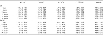
For the thru-plane measurements, shown in Fig. 3(c), a single equivalent circuit fits the impedance data found for the different layered CB samples. This circuit, which will be referred to as the “nested-R-CPE,” describes the mechanism of current flow through the paper composite when the thru-plane properties are dominated by the pore structure of the paper. There is a dense layer of conducting material (R 1–C 1) near the surface which is followed by a more sparsely CB coated region along the paper fibers in the pore network of the paper (R 2-CPE2). In looking at Fig. 3(c), it would seem as though there were no trends with the number of deposited layers; however, the values of the equivalent circuit presented in Table II show otherwise. As the number of CB deposited layers increase, R 1, the resistance of the dense near-surface region decreases, whereas R 2 remains relatively constant. There is a nearly constant deposition of CB within the paper structure, which likely occurs within the first few layers, as suggested by the constant R 2 value for all the layer numbers. The decreasing R 1 with layer number suggests that the CB is more likely to deposit around other CB particles near the surface of the paper rather than continue to deposit inside the paper structure.
Equivalent circuit values for the circuit in Figs. 3(c) and 6(c) corresponding to the thru-plane impedance behavior for 1–20 deposited layers of CB and SWNTs on paper.

B. Electrical properties of MWNT and paper composites
Figure 4 provides the in-plane (4a and 4b) and thru-plane (4c) impedance responses for the different number of deposited MWNT layer composites on the 1-µm paper. Although up to 4 different equivalent circuits have been detected for similar films deposited onto 5-μm pore size substrates, for the MWNT/paper composites in this paper, only two different electrical responses were detected for the in-plane. Because the MWNTs and the pore size of the paper are about equal in size in this study, an interconnected film forms with the first deposited layer.
The impedance response presented in Fig. 4(a) for the 1 layer and 4 layer deposited MWNT composites is described by the “Nested-RL” circuit, which was described in great detail in Ref. Reference Muhlbauer, Joshi and Gerhardt20 as thin-film behavior of MWNT films deposited on paper substrates. The values of the circuit components are available in Table III. The choice of the nested-RL circuit, which appears for lower density, but fully interconnected CNT films, is substantiated from the image of the 4-layer MWNT composite surface in Fig. 1(c), which shows that the MWNT film is interconnected, but there are still small regions of paper visible (upper left corner).

The inductor (L 1) is active at high frequencies (between 10 and 21 MHz) and, as stated before, is likely an artifact of the instrumentation. The behavior of the MWNT film and film components is described by the rest of the circuit. First, there is a high frequency parallel R–C (R 1–C 1), which describes MWNT bundle behavior. The resistance of the bundles (R 1 = ∼900 Ω) matches those reported in a previous publication, Reference Muhlbauer, Joshi and Gerhardt20 which is expected since the same type of MWNT was used in this experiment. The low frequency parallel R–C (R 2–C 2) describes the MWNT–MWNT junction behavior. R 2 decreases with increasing layer number, indicating that the quality of the junctions between tubes is improving as more layers are deposited.
The third semicircle, appearing at very low frequencies and fitted by the parallel R–L (R 3–L 2), elucidates the behavior of the coiled MWNT bundles. Reference Muhlbauer, Joshi and Gerhardt20 The interaction of the MWNTs with the paper fibers causes some of the bundles to obtain a curvature to match that of the paper fiber. Unlike the bundle resistance, which is constant for both 1 and 4 layers of MWNTs, the coiled bundles decrease in resistance by an order of magnitude as the layer number is increased, as shown in Table III. As more layers are added, it is likely that the degree of curvature of the bundles is overall decreased. The increased number of layers of MWNTs results in fewer coiled bundles at the surface which are not as curved.
Bulk metallic behavior of the MWNTs begins at 8 deposited layers, as shown in Fig. 4(b) and described by a series R–L circuit. Reference Gerhardt, Bassani, Liedl and Wyder26 The resistance of the surface decreases from 1268 Ω at 8 layers to 143 Ω at 20 layers. An example of a bulk metallic MWNT surface microstructure is available in Fig. 1(d) and also in Fig. 4(d).
For the thru-plane, only a single circuit is required to fit the impedance response for all of the MWNT composites deposited on the 1-μm size paper: a resistor in parallel with a constant phase element. This circuit represents the behavior of a fully interconnected MWNT structure in the thru-plane of the composites which is not dominated by the pore location, as was the case for the CB composites. The resistance decreases from 963,994 ± 10,190 Ω at 1 layer to 47,074 ± 1443 Ω at 20 layers. The values of the constant phase element were relatively constant for all layer numbers with τ ≈ 10−10 s and β ≈ 0.85.
C. Electrical properties of graphite and paper composites
Figure 5 shows the impedance responses of the in-plane and thru-plane for the multilayered-graphite and paper composite materials. The in-plane response of the graphite flake–paper composite films shows an evolution in impedance behavior, shown in Figs. 5(a)–5(c). At low graphite flake loading [1 and 4 layers, Fig. 5(a)], a single parallel R–C circuit is assigned to the behavior of the composites with resistances of 2.42 × 10⁹ ± 1.16 × 10⁸ Ω and 1.27 × 10⁹ ± 6.8 × 10⁸ Ω for 1 layer and 4 layers of graphite, respectively. In both cases, the capacitor has a value of ∼2 × 10⁻¹² F. Such a high resistance value indicates that the dominant mechanism of electrical transport is through the paper fibers. Figure 1(e) shows a pocket of graphite particles on the surface of the paper for the 4-layer graphite sample; however, at lower magnification, the pockets are separated by paper fibers (not shown).
At 8 and 12 layers, graphite thin film behavior dominates the electrical behavior of the composites. The circuit values for the equivalent circuit in Fig. 5(b) are reported in Table IV. The fit is two parallel R–C's in series with a high frequency inductor possibly related to instrumentation. R 1–C 1 represents the conduction through the dense graphite pockets, whereas R 2–C 2 probably represents the conduction between graphite flakes in between dense areas. Both R 1 and R 2 decrease by an order of magnitude as the number of layers is increased from 8 to 12 layers indicating an increase in the density of the graphite film. At 16 and 20 layers, the bulk metallic behavior of graphite dominates the in-plane response (series R–L) with a resistance of 1190 and 720 Ω, respectively, and an inductance of ∼5 × 10⁻⁶ H for both cases.
Equivalent circuit values for the circuit in Fig. 5(b), describing the in-plane thin film behavior of graphite deposited on paper.

For the thru-plane measurements, shown in Fig. 5(d), a single R-CPE parallel circuit describes the behavior of all the graphite and paper composites. Although the same circuit describes the thru-plane behavior for the MWNT and paper composites, the structure description is not the same. The graphite platelets are 5–10 µm in length, which is much greater than the pore size of the paper (∼1 μm). There is therefore very little deposition of graphite flakes happening within the paper structure. For uncoated paper, the electrical behavior through the thickness of the paper follows the same circuit, where R = 1.27 × 10⁷ Ω, Ƭ = 8.89 × 10⁻¹¹ s, and β = 0.901. For the graphite systems, the addition of graphite layers lead to the equivalent circuit values decreasing; however, because the particles are not coating the internal structure (this is confirmed within the thermal properties section), the surface layer is just enabling more current flow through the thickness of the layered graphite flake-paper films, causing the measured decrease in resistance from that of the pure paper.
D. Electrical properties of SWNT and paper composites
As shown in Figs. 6(a) and 6(b), the in-plane behavior of the SWNT dispersion deposited on the paper shows a similar behavior to that found for the MWNT and paper composites. Both systems exhibit the nested-RL [inset in Figs. 4(a) and 6(a)] and the bulk metallic response [inset in Figs. 4(b) and 6(b)] as the number of layers increases; however, the SWNT and paper composites switch from thin film to bulk behavior much earlier than the MWNT samples, at 4 layers. When the SWNTs are exhibiting thin film behavior, the SWNT bundle resistance is 485 Ω (R 1 in Table III), which is in agreement with bundle resistances found in a previous experiment on similarly prepared SWNT films made with much lower concentrations. Reference Garrett, Ivanov, Gerhardt, Puretsky and Geohegan28 For 4–20 deposited layers, the in-plane response of the SWNT and paper composites shows bulk metallic behavior, decreasing from 488.3 ± 92.1 Ω at 4 layers [microstructure shown in Fig. 1(g)] to a minimum of 44.2 ± 12.1 Ω at 16 layers and 66.9 ± 22.2 Ω at 20 layers [microstructure shown in Figs. 1(h) and 6(d)]. For all composites between 4 and 20 deposited layers, the measured inductance fell between 4.3 and 6.4 µH.
The thru-plane of the SWNT–paper composites, shown in Fig. 6(c) and Table II, while described by the same circuit as most of the other graphitic fillers reported above, behave surprisingly very differently. As the number of layers deposited increases, R 1, the resistance across the thickness of the film increases instead of decreasing. It has been proposed that such a behavior may be due to the presence of an increasing number of Schottky barriers, which are believed to arise between the semiconducting and metallic tubes, as the number of layers increases. Reference Fuhrer, Nygard, Shih, Forero, Yoon, Mazzoni, Choi, Ihm, Louie, Zettl and McEuen29 However, it is also possible that excess surfactant which cannot be filtered all the way through the SWNT layers may be impeding current flow through the thick surface film. R 2 remains relatively constant for all of the samples, although it is larger than the resistance measured for the thru-plane of uncoated paper. It is speculated that the combined effect of the length of the SWNTs and the remnant surfactant may be causing the increase in measured resistance of the films.
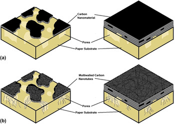
Figure 7 displays a pictorial model of the microstructure of all of the composite films made by dropcasting using the same dispersion concentration of graphitic fillers onto the same filter paper using vacuum filtration from the detailed analysis described above using impedance spectroscopy. Figure 7(a) gives a good representation of what occurs for the CB and graphite flake composites, whereas Fig. 7(b) displays the response for the short MWNTs we worked with. The SWNT-paper films straddle these two schematics well by showing a fully in-plane interconnected SWNT film, but the thru-plane is not expected to show any SWNT infiltration of the paper pores through the substrate thickness. The differences can be ascribed to the fact that the MWNT we used were fairly short (0.5–2 μm), whereas the length of the SWNT nanotube bundles we used were too large (>10–20 μm) to allow infiltration of the small 1-μm pore size of the paper substrates as shown in Fig. 7(b).
Schematics representing the microstructural details of the composite films fabricated and measured. (a) Schematic representation of the structure occurring for CB and graphite flakes. (b) The microstructure of the MWNT composite films. SWNT composite films are not shown but are described in the text.

E. Thermal properties of the carbon nanomaterial-paper layered composites
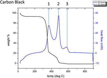
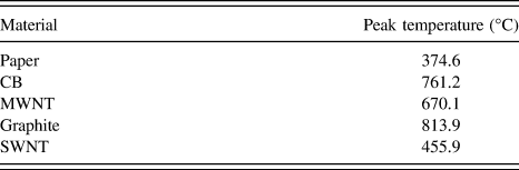
To determine what effect the different carbon nanomaterials had on the thermal properties of the coated paper, DSC/TGA scans were completed and weight (%) and heat flow (W/g) were plotted versus temperature. The maximum peak positions in the heat flow versus temperature graphs corresponded to the temperature at the end of a weight loss event, and up to 3 peaks were seen for each sample. Figure 8 displays the TGA/DSC curves for the CB-coated paper specimens, which is representative for all of the nanomaterials used. The thermal events show the presence of 3 peaks that appeared at different temperatures for the different graphitic fillers. Table V shows the peak temperature for the pure paper and pure nanopowder samples. At the temperatures presented in Table V, 100% of the powder material was gone.
Representative TGA/DSC curve for the CB-paper specimens with 20 layers. Thermal decomposition processes are labeled as peak 1, 2, and 3.

Temperature at the peak position of the heat flow versus temperature graphs for the different pure materials corresponding to the end of a weight loss event.

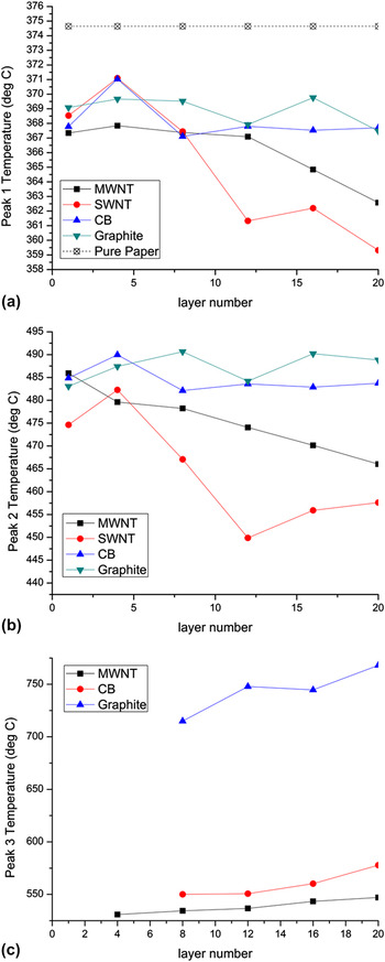
Figure 9 summarizes the peak temperature trends for all of the films observed in all cases. The peak temperatures for nominal peak 1, peak 2, and peak 3 are plotted versus the number of layers of carbon nanomaterial for each composite system. Figure 9(a) shows the temperature corresponding to only paper weight loss which can be detected in all of the layered film composite systems. In each case, the temperature measured for the composite event was lower than the temperature found for the pure paper. Additionally, although the peak temperature for the CB and the graphite composites remained relatively constant with the layer number, the MWNT and SWNT composites trended downward with the number of layers. It is likely that the high thermal conductivity of MWNTs and SWNTs (see Ref. Reference Hone and Dekker30) resulted in faster thermal degradation in these materials.
Peak temperature versus number of layers of carbon nanomaterial deposited on each composite film set: (a) paper weight loss peak; (b) the carbon material/paper/surfactant interface or SWNT powder weight loss peak; and (c) the powder weight loss peak. The leftover powder weight loss peak only appears when there is enough powder not associated with the paper backbone leftover during the thermal cycle.

Figure 9(b) shows the position of the middle peak that appears for the layered coated paper composite materials. Through a systematic study of the different variables that could cause this peak, it was found that the middle peak describes the weight loss event for the paper fibers, which have both carbon material and SDBS material on it (except for the SWNT samples). In the case of the graphite material, the actual weight loss for this peak is much lower than for the other materials (∼12% for all of the composites), and it is much more constant across the layers, suggesting that the graphite peak is due to the interface region between the paper and graphite. About 20–30% of the weight loss of the composites for the MWNT and CB composites occurs at this peak temperature. In the case of the SWNT material, the weight goes to zero after this peak event suggesting that the high very thermal conductivity of the SWNTs leads to this event encompassing both the loss of the coated paper fibers as well as the SWNT powder. Similar to peak 1, as the number of layers increases, the temperature of the weight loss event for the CB and graphite composites remains constant, whereas the peak temperature for the MWNT and SWNT composites decrease faster again likely due to the high thermal conductivity of these samples.
Figure 9(c) shows the position of the last peak (labeled peak 3 in Fig. 8, which can appear for these materials). This peak is only visible when there is sufficient powder not associated with a paper surface. In addition, the temperature of the peak position increases with the number of layers of the carbon nanomaterial deposited and trends toward the peak position of the pure powder.
IV. CONCLUSIONS
The combination of microscopy, AC electrical properties characterization, and thermal property characterization allows for the detailed determination of the composite properties of layered carbon nanomaterials deposited onto the same type of paper substrates with nominal 1-μm pore size. For the in-plane electrical property measurements, it was possible to observe the evolution of the electrical response of the films from highly insulating like paper-dominated response to much more conducting thin film response to bulk metallic electrical behavior in the composites containing MWNTs and SWNTs. In the case of graphite flakes and CB, the electrical response was much more affected by the underlying paper substrate, although at sufficient thickness, the graphite flake films percolated in-plane and gave reasonable low resistances, which did not happen with the CB used. The assignment of the equivalent circuit components to physical components of the films was aided by SEM micrographs of the film surfaces.
For the thru-plane electrical properties, equivalent circuit fitting allows for the determination of the internal structure of the paper composites. For the MWNT and paper composites, the MWNTs are located densely throughout the composite film. For the CB and SWNT composites, a separate resistance can be determined for the surface and the internal structure of the paper. The graphite flakes are located only on the surface, and the decreased resistance is a function of the increased thickness of the stacked graphite flakes that aid current flow throughout the thickness of the composite.
The carbon nanomaterial–paper composite films exhibit up to three distinct weight loss events. All of the composites experience the first weight loss event, which is due to the loss of the pure paper. The second weight loss event can either correspond to the paper/SDBS/carbon material (MWNT, CB, or graphite) burn-off event or the loss of SWNT powder. For the first and second peak, the temperature of the peak is relatively constant for the CB and graphite composites but decreases with increased loading of MWNTs and also SWNT due to the excellent thermal conductivity of the material. The third weight loss event only appears when there is enough material accumulated which is not associated with the paper backbone.
ACKNOWLEDGMENTS
The authors would like to acknowledge the Georgia Tech IGERT: nanomaterials for energy storage and conversion for RLM's support. Research funding from the National Science Foundation under DMR-1207323 is acknowledged and appreciated for TLP and WTP. RAG would also like to acknowledge the Center for Nanophase Materials Sciences at Oak Ridge National lab and in particular, Matthew Garrett and Ilia Ivanov for sharing some of their precious SWNT nanomaterials.