Plasmonics and dense optical integration
Surface plasmon polaritons (SPPs) are quasiparticles comprised of collective electron oscillations coupled to electromagnetic waves at the interface between two materials with positive and negative permittivity; typically, a dielectric and a metal. The use of a plasmonic waveguide allows for stronger optical confinement and denser integration of photonic integrated circuits (PICs).
The integration of different optical components on one substrate has many advantages. Similar to electronic devices, an integrated optical circuit will have a lower cost and better functionality. In the case of electronic circuits, the small size of semiconductor transistors means that millions of transistors can be integrated into one electrical circuit. Integrated electronic devices have complex functionalities and low cost because of this dense integration of components. However, the size of optical components is a problem for dense integration of optical circuits. The length of an optical component is limited by the wavelength of light, the relatively long length of interaction between light and matter (e.g., the magneto-optical [MO] or electro-optical interaction), and the large minimal bending radius of an optical waveguide. Because of these limitations, only a few optical components can be integrated into one chip.
It is possible to substantially reduce the size of optical components when an optical waveguide with strong optical confinement, such as a Si nanowire waveguide or a plasmonic waveguide, is used. The optical confinement in a Si nanowire waveguide is strong, due to a high-refractive-index contrast between Si and SiO2. Because of the strong optical confinement, a Si nanowire waveguide is narrow, with a typical width of 450 nm, and it can be sharply bent with a radius as small as 1 μm. Even though the length of a Si nanowire device is relatively long, the optical device can be packed into a small area of a few square micrometers by the bending of the waveguides. Optical confinement in a plasmonic waveguide is even stronger than in a Si nanowire waveguide, because a plasmon is confined by a metal–dielectric interface, and the refractive index step between a metal and dielectric is large. Therefore, the size of optical components made of a plasmonic waveguide is even smaller than the size of optical components made of a Si nanowire waveguide.
Plasmonic isolator
The optical isolator is an important element of optical networks.Reference Stadler and Mizumoto1 It protects optical elements from unwanted back reflection. The integration of optical elements into PICs is important—it reduces cost and improves performance of high-speed optical data-processing circuits for high-speed optical networks. In achieving denser integration, the optical isolator is an indispensable component, because the problem of unwanted back reflection increases as integration becomes denser.
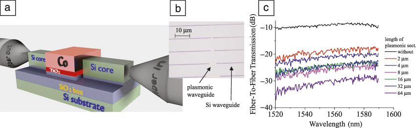
Figure 1a shows an example of a proposed design for a plasmonic isolator.Reference Zayets, Saito, Yuasa and Ando2,Reference Zayets, Saito, Ando and Yuasa3 It consists of a Si nanowire waveguide, part of which (about 2–16 µm) is etched out, and a ferromagnetic metal (Co) is deposited in the gap. The ferromagnetic metal is not transparent and the direct light propagation from the input Si waveguide to the output Si waveguide is blocked by the Co. However, a surface plasmon is excited at the Co-TiO2-SiO2 interface, which transmits light into the opposite waveguide and output optical fiber.
(a) Integration of a plasmonic waveguide with a Si nanowire waveguide. From input fiber (at right), light is coupled into a Si nanowire waveguide (green) and into a plasmonic waveguide. Next, light is coupled again in a Si nanowire waveguide and finally into the output fiber (at left). (b) Top view in an optical microscope of Si nanowire waveguide integrated with plasmonic waveguides. (c) Fiber-to-fiber transmission as a function of wavelength for different lengths of Co-TiO2-SiO2 plasmonic waveguides integrated with a Si nanowire waveguide. The black plot shows the case of a Si waveguide without the plasmonic section.

Co is a MO material. When its magnetization is perpendicular to the direction of light propagation and is in the plane of the film, its optical constants are different for two opposite light propagation directions. The plasmonic waveguide is optimized so that a plasmon is excited in one direction, but a plasmon is not excited in the opposite direction. Light can pass from input to output only in the forward direction, but light is blocked in the opposite direction. The device, which is transparent only in one direction, is called an optical isolator. Figure 1b shows a top view of Co-TiO2-SiO2 plasmonic waveguides of different lengths integrated with Si nanowire waveguides. The figure shows the fiber-to-fiber transmission function as a function of wavelength for different lengths of the Co-TiO2-SiO2 bridge-type plasmonic waveguide integrated with a Si nanowire waveguide. The measured propagation loss is 0.7 dB µm and the measured coupling loss between the plasmonic and Si nanowire waveguides is 4 dB per facet.
Plasmonic isolator of the ring-resonator type
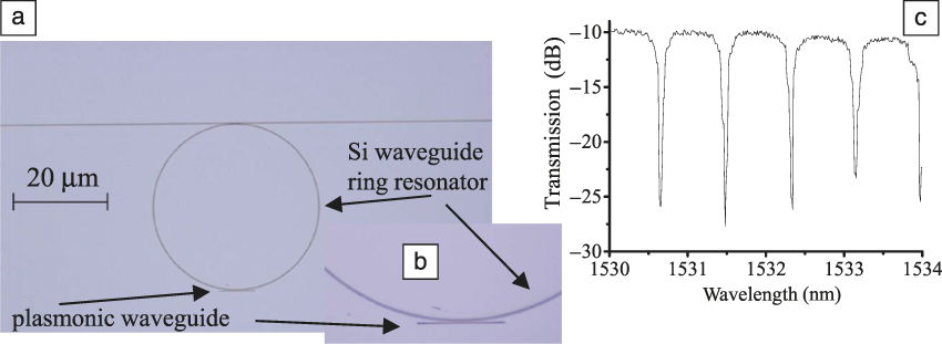
Figure 2a shows a fabricated plasmonic isolator of the ring-resonator type. The ring resonator is made of a Si nanowire waveguide, and at the bottom of the ring is a plasmonic waveguide.Reference Zayets, Saito and Yuasa4 The gap between the ring and the plasmonic waveguide is narrow (50–600 nm), so light is coupled between them. Figure 2b shows the measured transmission of the fabricated device. There are narrow peaks, which correspond to the resonance frequency of the ring resonator. The positions of the resonance peaks are slightly different for opposite directions of light propagation because of the nonreciprocal optical properties of the plasmonic waveguide. When the wavelength is in the vicinity of a resonance peak, the transmission is different for opposite directions of light propagation and the device functions as an optical isolator.
Plasmonic isolator of ring-resonator type. (a) Top view. The ring resonator is made of a Si nanowire waveguide. At the bottom, there is a plasmonic waveguide, which is coupled to the ring. (b) Magnified view of the plasmonic part. (c) Transmission of the ring resonator, when the gap between the ring and plasmonic waveguide is 600 nm. The negative peaks correspond to the resonant wavelengths, and the depth corresponds to the degree of resonance (cavity loss).

Plasmonic isolator based on a Mach–Zehnder interferometer
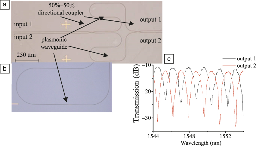
Figure 3a shows the fabricated plasmonic isolator based on a Mach–Zehnder interferometer constructed from a Si nanowire waveguide.Reference Zayets, Saito and Yuasa4 The input light is split into two arms of the interferometer by a 50% directional coupler. At the output, the light from both arms is combined by a second 50% directional coupler. When there is no phase difference between the light passing through each arm, the combined light is coupled into the first output port. When the phase difference is 180°, the light is coupled into the second output port.
Plasmonic isolator based on a Mach–Zehnder interferometer. (a) Top view of the device. (b) Magnified view of the plasmonic waveguide in the lower arm. (c) Transmission of the asymmetric interferometer versus wavelength. The gap between the ring and plasmonic waveguide is 600 nm. The difference in length of the interferometer arms is 200 μm.

A plasmonic waveguide is in the vicinity of each arm of the interferometer. The gap between the interferometer arm and the plasmonic waveguide is between 50 nm and 600 nm—sufficiently narrow for light to couple between the Si and plasmonic waveguides, and is different for the upper and lower arm. Although the two plasmonic waveguides are magnetized in the same direction, their magnetization directions are different with respect to the direction of light propagation. If the magnetization direction for the upper arm is toward the left, the magnetization direction of the lower arm is toward the right. Therefore, light experiences the opposite MO effect in the two arms of the interferometer. As a result, the phase difference between light passing in each arm is 0° in the forward direction and 180° in the backward direction. In the forward direction, light passes from the input to the output. The unwanted reflected light in the backward direction is blocked from the input.
Critical technologies to fabricate a low-loss plasmonic waveguide
A metal is an essential material in a plasmonic waveguide.Reference Baryshev and Merzlikin5,Reference Armelles, Cebollada, García-Martín and González6 Any metal significantly absorbs light. Therefore, some optical loss is unavoidable in a plasmonic waveguide, but if the loss is too large, all of the light can be absorbed. Even if the plasmonic waveguide has a unique property, it has no practical use in this case. Therefore, any practical plasmonic waveguide should have a reasonably low propagation loss. We have found that both effective in-plane and out-of-plane optical confinement are critically important to fabricate a low-optical loss plasmonic waveguide.
Out-of-plane confinementReference Zayets, Saito, Yuasa and Ando2,Reference Zayets, Saito, Ando and Yuasa3,Reference Zayets, Saito, Ando and Yuasa7–Reference Ignatov, Merzlikin, Baryshev, Zablotskiy and Kuzin9 is important because it minimizes the loss due to the absorption of light in the bulk of a metal. Since a metal absorbs light, the less light inside the metal and the more light inside the dielectric, the smaller the propagation loss. For the simplest plasmonic structure that consists of one dielectric covered by a metal, the ratio between amounts of light inside the dielectric and metal is fixed by the dielectric constants of each material and is not optimized. In contrast, in a double-dielectric or multidielectric plasmonic structure, the thickness of one dielectric can be optimized so that the amount of light in the metal becomes smaller and the amount of light in the dielectric becomes larger. This reduces the propagation loss of the surface plasmon.Reference Zayets, Saito, Yuasa and Ando2,Reference Zayets, Saito, Ando and Yuasa3,Reference Ignatov, Merzlikin, Baryshev, Zablotskiy and Kuzin9 The reduction of optical loss in plasmonic structures with an optimized multilayer dielectric is very effective, and can be 10 or even 100× smaller than in a similar plasmonic structure with a single dielectric.Reference Zayets, Saito, Yuasa and Ando2,Reference Zayets, Saito, Ando and Yuasa3
Enhancement of MO effect for a plasmon near cutoff
The unique feature of a surface plasmon is that its properties significantly depend on the conditions at the dielectric–metal interface. Even a slight change in the condition at the interface may significantly alter the properties of the plasmon. As previously discussed, the insertion of a thin dielectric layer at the interface reduces the propagation loss of a plasmon by 10–100×. Similarly, a slight change of refractive index due to the MO effect may drastically change the properties of a plasmon, which in turn causes a large enhancement in the MO effect.
When a thicker dielectric layer is inserted at the interface, the distortion of the plasmon is too large and plasmon propagation is not supported.Reference Zayets, Saito, Yuasa and Ando2,Reference Zayets, Saito, Ando and Yuasa3,Reference Kaihara, Ando, Shimizu, Zayets, Saito, Ando and Yuasa10 The boundary conditions at which a plasmon is no longer supported are called plasmon cutoff conditions. Due to the MO effect, the cutoff thickness is different for a plasmon propagating in two opposite directions. When the thickness of the dielectric insertion layer is between these two cutoff thicknesses, a plasmon can propagate in the forward direction, but not in the opposite direction. In this “ideal” case, the MO effect is infinite.
Experimental demonstration of enhancement of the MO effect for a plasmon
In the case of a ferromagnetic metal, the MO effect is relatively weak and the difference between the cutoff thicknesses of plasmons propagating in opposite directions is relatively small. This limits the thickness variation of the insertion layer to about 1∼10 nm. The plasmonic waveguides in Figures 1–3 were fabricated using the liftoff technique, but it is difficult to obtain the required low variation in thickness using this technique because of the photomask-shadow effect. However, it is possible to meet this requirement in the case of a plain film composed of an Al2O3-SiO2-Fe structure, where the SiO2 and Fe layers are deposited on an Al2O3 substrate by electron-beam evaporation and sputtering.
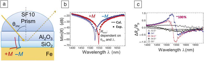
We have demonstrated 100% enhancement of the MO figure of merit (FOM) using a plain film with an optimized double-dielectric structure where a dielectric layer of lower refractive index (SiO2, thickness t = 753 nm) is inserted between the dielectric layer of higher refractive index (Al2O3 substrate) and the ferromagnetic metal (Fe) layer.Reference Kaihara, Shimizu, Cebollada and Armelles11 A prism of SF10 glass with the same refractive index as that of Al2O3 is used to match the in-plane propagation constants of light and the plasmon. At the matched incident angle θinc of light, a plasmon is excited and the intensity of the reflected light for p-polarized light is reduced. Therefore, there is a dip in the intensity of the reflected light as a function of the incident angle corresponding to surface plasmon resonance. When the magnetic field is reversed, the position and width of the dip changes, because of the change in plasmon propagation constant and the propagation loss due to the MO effect.
For each wavelength, the reflectivity minimum and its corresponding angle are different. Figure 4b shows the minimum reflectivity Min(R) as a function of wavelength at its corresponding angle for two opposite magnetization directions (+M/−M). There is a clear resonance wavelength, at which the reflectivity becomes nearly 0. It indicates the lowest plasmon propagation loss occurs at this wavelength. As previously discussed, the reduction of the plasmon propagation loss is due to the optimized out-of-plane confinement of a plasmon by the optimized double-layer dielectric structure. The most efficient reduction is near the cutoff condition at a wavelength of 1550 nm. This is the reason why reflectivity of nearly 0 is observed in Figure 4b. Additionally, the peak wavelength is substantially different for the two opposite magnetization directions. This means the plasmon propagation loss is substantially different for the two directions, and the MO effect for the plasmon is substantial and significantly enhanced in this wavelength region.
Excitation of a plasmon by a prism. (a) A schematic diagram of the fabricated Al2O3-SiO2-Fe structure. An SF10 (glass) prism is mounted on top of the Al2O3 substrate, and the light is coupled with an incident angle θinc. The reflectivity measured under positive and negative magnetic field (+/−M) is applied by an electromagnet. Schematic plasmonic mode profiles in the structure are shown by red (+M) and blue (−M) curves. (b) Minimum reflectivity Min(R) as a function of wavelength for opposite magnetization directions (red and blue dots). Note that the reflectivity minimum and its corresponding angle are dependent on wavelength. The calculated reflectivity spectra are shown for comparison by the solid lines. (c) Relative reflectivity change (the magneto-optical figure of merit) ΔR p/R p under opposite magnetization directions (+M /−M) for different light incident angles. Adapted with permission from Reference Reference Kaihara, Shimizu, Cebollada and Armelles11. © 2016 American Institute of Physics.

Figure 4cReference Kaihara, Shimizu, Cebollada and Armelles11 shows the MO FOM, which is measured at various fixed incident angles as a function of the wavelength. The FOM ΔR p/R p is defined as a ratio of the reflectivity difference, ΔR p = R p(+M) − R p(−M), for two opposite magnetization directions to the average reflectivity, R p = R p(+M) + R p(−M). For incident angles of 54 and 54.10°, there are positive and negative peaks corresponding to the plasmon resonance for positive and negative magnetizations, at which there is a complete match of the propagation constants between the SPP and the in-plane component of the wave vector of incident light, and nearly zero propagation loss of the plasmon for each magnetization direction (for an incident wavelength of around 1550 nm). The larger the magnitude of peak ΔR p/R p, the larger the MO effect and the smaller the loss experienced by the plasmon. As shown in Figure 4c, ΔR p/R p approaches +1, and −1. The peak of ΔR p/R p is high only in a very narrow range of incident angles of about 0.1°. This corresponds to the enhancement of the MO effect by plasmon resonance which only occurs near the cutoff conditions. Outside this range, the peak of the ΔR p/R p is small and broad, because of a weak MO effect and larger loss associated with a plasmon at far from cutoff conditions.
Amplification of a plasmon: Hybrid structure of the isolator
Even though the propagation loss of a surface plasmon can be significantly reduced using the previously discussed techniques of the out-of-plane confinement, some plasmon propagation loss is unavoidable because of light absorption by the metal. Additionally, the coupling efficiency between a conventional dielectric waveguide and a plasmonic waveguide is still substantial (Figure 1b) due to a large difference in field distributions of a waveguide mode and a plasmon. As a result, the total insertion loss of the present plasmonic isolator is relatively large. One possible solution is the use of optical amplification of the plasmon. For example, when a ferromagnetic metal is deposited on top of an optical amplifier, the gain of the amplifier compensates the plasmon propagation loss and the coupling loss. However, there is a problem with this approach. The gain media has a relatively large refractive index and there is a substantial optical confinement in the gain region (e.g., in the vicinity of the quantum wells).Reference Zaets and Ando12 As a result, the optical mode in the structure is more “waveguide-like” than “plasmon-like.” The major advantage of a plasmon, which is the significant influence of conditions at the metal–dielectric interface on the plasmon propagation constants, partially diminishes in this case. Because of this, the combination of an optical amplifier with a ferromagnetic electrode is often called a hybrid isolator.
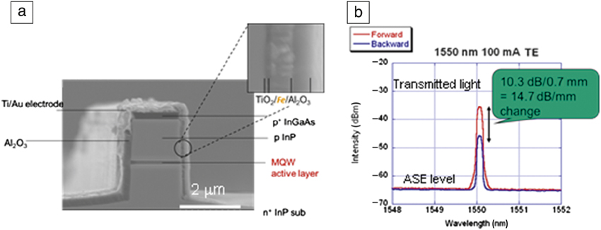
A conventional optical amplifier operates only for light in the transverse electric (TE) polarization, which is directed in-plane. The polarization of a plasmon is transverse magnetic (TM), which is directed perpendicularly to the metal interface. Therefore, for the amplification of a plasmon, a metal should be deposited at a side wall of the amplifier. Figure 5a shows a cross-sectional scanning electron microscope image of a TE-mode hybrid isolator, where 100-nm-thick Fe and 30-nm-thick TiO2 layers were deposited on one of the InP-based semiconductor optical amplifier (SOA) waveguide side walls. The device length was 0.7 mm. Figure 5b shows the transmission of the TE-mode laser light (λ = 1550 nm), with a forward bias current of 100 mA. The difference of the transmission for two opposite light propagation directions was 10.3 dB, which corresponds to an isolation of 14.7 dB/mm.Reference Shimizu and Nakano13,Reference Shimizu and Nakano14 We also demonstrated integration of a TE-mode hybrid isolator with a single-mode distributed feedback laser.Reference Shimizu and Nakano15 A tensile-strained quantum well can be used to achieve optical amplification for TM-polarized light. In this case, a ferromagnetic metal is deposited on top of the optical amplifier waveguide.Reference Zayets and Ando16–Reference Zayets and Ando26
(a) Cross-sectional scanning electron microscope (SEM) image of an InGaAsP/InP optical amplifier with Fe deposited on one side wall. The optical amplifier is composed of a multiple quantum well (MQW) active layer sandwiched with p- and n-type InP cladding layers. (b) Optical transmission of transverse electric (TE)-mode laser light (λ = 1550 nm), with a forward bias current of 100 mA injected from a Ti/Au electrode through a heavily p-type (p+) InGaAs contact layer. Red and blue plots correspond to opposite directions of light propagation. The difference is due to the magneto-optical effect in Fe. The broad background signal is from amplified spontaneous emission (ASE) from the optical amplifier. Adapted with permission from Reference Reference Shimizu and Nakano14. © 2006 IEEE and Optical Society of America.

Future prospects
Further reduction of the plasmon propagation loss and enhancement of the MO effect is important for developing a practical plasmonic isolator. We have proposed the use of the long-range dielectric-loaded surface plasmon polariton waveguide configuration.Reference Kaihara and Shimizu27 In this case, a thin layer of the ferromagnetic metal is used, and the plasmon propagation loss can be significantly reduced and the MO effect can still be substantial.
It is possible to enhance the MO effect by combining a highly conductive Au layerReference Armelles, Cebollada, García-Martín and González6 with a ferromagnetic Fe layer in hybrid plasmonic Si waveguides.Reference Shimizu and Shimodaira28 The insertion of the Au layer enhances the optical confinement and it reduces the plasmon propagation loss due to a lower ohmic loss in the Au.
Conclusions
This article discussed current developments of the plasmonic isolator and the integration of the plasmonic isolator into PICs on Si and InP substrates. The ability to enhance the MO effect is a unique and important property of a surface plasmon. The plasmonic isolator benefits dense optical integration because of its small size and its good compatibility with present fabrication technology of PICs.
Acknowledgments
We thank G. Armelles and A. Cebollada of CNM-CSIC, Spain, for their collaboration and discussions on plain-film plasmonics by using prism coupling. This work was partially supported by a Grant-in-Aid for Scientific Research (No. 16H04346) from the Japan Society for the Promotion of Science.

Hiromasa Shimizu is an associate professor in the Department of Electrical and Electronic Engineering at the Tokyo University of Agriculture and Technology, Japan. He received his BSc degree in 1997 and his PhD degree in 2002, both in electronic engineering from The University of Tokyo. His research focuses on magneto-optics, waveguide optical isolators, photonic integrated circuits, and optical sensing applications. Shimizu can be reached by phone at +81-42-388-7996 or by email at h-shmz@cc.tuat.ac.jp.

Vadym Zayets is a senior research scientist in the Spintronics Research Center at the National Institute of Advanced Industrial Science and Technology (AIST), Japan. He received his PhD degree in physics in 1995 from Kiev University, Ukraine. His research focuses on spin-photonics, optical nonreciprocal devices, high-speed optical memory, nonvolatile memory, and features of spin transport in a metal. Zayets can be reached by phone at +81-298-61-5426 or by email at v.zayets@aist.go.jp.