I. INTRODUCTION
Wireless power transfer (WPT) is a way of transferring power from one device to another device without any wire or cable connections [Reference Tseng, Novak, Shevde and Grajski1–Reference Li, Tsui and Ki5]. The technology has become increasingly important with the development of various customer electronics that require frequent charging with very different charging requirements and equipment. Loosely coupled systems [Reference Tseng, Novak, Shevde and Grajski1, Reference Stielau and Covic6–Reference Fotopoulou and Flynn8] provide freedom of movement, but they suffer from lower-power transfer efficiencies compared to their strongly coupled counterparts. Applying resonance to the system will increase the power transferred if a robust tuning of both primary and secondary can be achieved and kept. Based on the application and the system, different resonance frequencies are used such as 100 kHz, 6.78 MHz [Reference Tseng, Novak, Shevde and Grajski1–Reference Dai and Ludois3], and 13.56 MHz [Reference Lu, Li, Ki, Tsui and Yue4, Reference Li, Tsui and Ki5]. In this paper, two different cap structures are applied to a WPT system to re-tune the circuitry at 13.56 MHz. Section II gives background about inductively coupled systems (ICS). Section III analyzes MOS cap structures. Details of the proposed cap structures are given. Methodology and simulations results are summarized in Section IV. Conclusion is given in Section V.
II. INDUCTIVELY COUPLED SYSTEMS
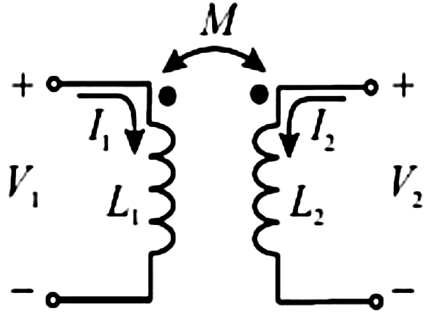
In ICS [Reference Stielau and Covic6–Reference Fotopoulou and Flynn8]; the creation of a magnetic field in the near-field of the antenna is the key. The changing magnetic field creates an alternating current (AC) in the primary side. The AC induces a voltage onto the secondary side which in return creates an AC current. Induced voltage is described by Ampere's and Faraday's Laws. Rectification of the AC current on the secondary side results in direct current (DC). Later the DC current is used to charge a load (usually a battery). ICS use mutual inductance (M) model where induced and reflected voltages define the coupling between the primary and secondary. A simple circuit equivalent of an ICS is shown in Fig. 1.
 $${V_1} = j(2\pi f){L_1}^{\ast}{I_1} + j(2\pi f)M^{\ast}{I_2},$$
 $${V_2} = j(2\pi f){L_2}^{\ast}{I_2} + j(2\pi f)M^{\ast}{I_1}.$$
Mutually coupled inductors.

Induced voltages both at primary and secondary sides can be expressed in terms of M as seen in equations (1a) and (1b), where M is the mutual inductance, k is the coupling coefficient, f is the operation frequency, V 1 is the primary voltage, V 2 is the induced voltage in secondary, I 1 is the primary current, I 2 is the secondary current, L 1 is the self-inductance of primary, and L 2 is the self-inductance of secondary.
A) Leakage inductance
Leakage inductance is an inductive component that is present in an ICS. Any magnetic flux that does not link the primary side to the secondary side will not have any role in system's power transfer action. This kind of flux will act as inductive impedance in the circuit and called “Leakage inductance”. Loosely coupled systems suffer from leakage inductance (might be larger than the mutual inductance) because of low-coupling coefficient (k < 0.1) and substantial air gap [Reference Tseng, Novak, Shevde and Grajski1, Reference Stielau and Covic6–Reference Fotopoulou and Flynn8]. By all means, coupling coefficient in equation (2) will vary based on the distance or the alignment of the coils [Reference Stielau and Covic6–Reference Fotopoulou and Flynn8].
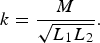 $$k = \displaystyle{{{M}} \over {\sqrt {{L_1}{L_2}}}}. $$
B) Compensation topologies
Different compensation topologies [Reference Zhou and Hao9, Reference Jegadeesan and Guo10] have been implemented in power systems for years to reduce the effects of leakage inductance therefore increasing the power transfer efficiency and capacity. Including the uncompensated scenario; there are nine common topologies where compensation capacitor is connected either in series or parallel at the primary and/or at the secondary.
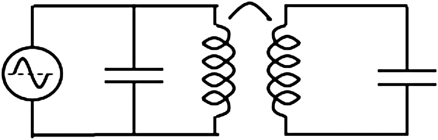
These topologies can be listed as UU (uncompensated primary, uncompensated secondary), US, UP, SU, PU, SS (series primary, series secondary), SP, PS, PP (parallel primary, parallel secondary in Fig. 2). It is also possible for primary to have compensation capacitors both in series and parallel at the same time. Based on the requirements and the application; any combination of these can be used. The proposed method in this paper can be used for all of the above topologies except UU.
Parallel primary–parallel secondary WPT System.
C) Resonance
In order to enhance the power transfer capability, many WPT systems use the resonance effect [Reference Mastri, Costanzo, Dionigi and Mongiardo11, Reference Rashidzadeh and Basith12] where primary and secondary sides resonate at the same frequency. The selection of this frequency changes based on the application, size, cost, and power requirements. Circuit mismatches, load, and magnetic coupling variations can cause deviation from the original f resonance which will require tuning of the circuitry to gain back the optimal working condition again.
III. MOSFET CAPACITORS
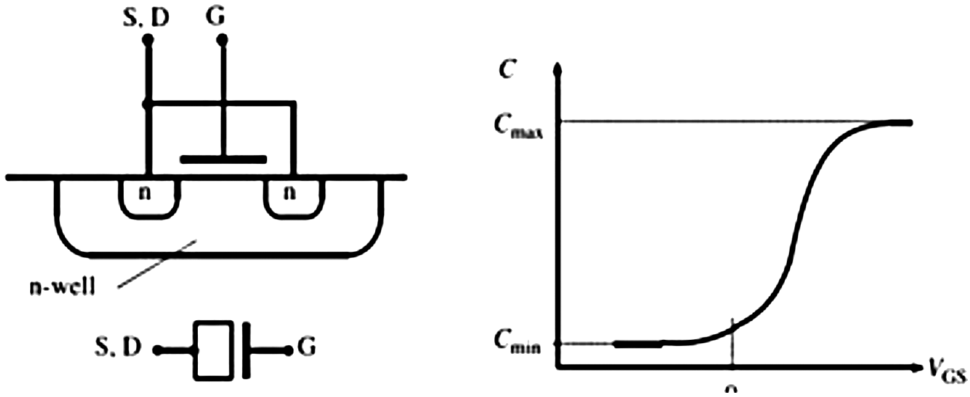
Various types of capacitors are used in IC design such as metal-insulated-metal (MIM) capacitors, diode-based capacitors, or MOSFET capacitors (MOSCAP). Among these capacitors, MOSCAP [Reference Mastri, Costanzo, Dionigi and Mongiardo11] can be used to minimize layout area. The bottom plate of the MOSCAP can be obtained by shorting drain and source terminals of MOSFET device while the gate will be the top plate of the capacitor. By changing the DC bias voltage at the bottom plate, the capacitance value can be varied [Reference Hu13]. Illustration of a MOSCAP along with its capacitance is shown in Fig. 3. Minimum and maximum values are given in equation (3).
 $${C_{\min}} = \displaystyle{{{ \in _{si}}} \over {{t_{dep}}}}\quad {\rm and}\quad {C_{\max}} = \displaystyle{{{ \in _{ox}}} \over {{t_{ox}}}},$$
where ∈si and ∈ox are the permittivity of the silicon and oxide, respectively. At the same time, t dep and t ox are the thickness of the depletion region in the silicon substrate and oxide between silicon and its gate. Depending on the voltage at the gate terminal (G) versus the source/drain (S, D) combined terminals, the MOSFET device travels in three different operating regions of accumulation, depletion, and inversion [Reference Hu13]. These regions basically carry either the same type of charge under channel as that of the bulk (in accumulation) or different types of charge (in inversion). The depletion region is the transitional operation between the accumulation and the depletion. Therefore, this device can be modeled as a capacitor since during the different operational regions charges at the channel varies based on the voltage potential difference between two terminals (G versus S/D). The variation of the capacitor is shown in Fig. 3. Typical value of the capacitor can be calculated using equation (4).
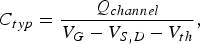 $${C_{typ}} = \displaystyle{{{Q_{channel}}} \over {{V_G} - {V_{S,D}} - {V_{th}}}},$$
where V G and V S,D are the voltages at the gate and source/drain terminals, respectively. V th is the threshold of the MOSFET device defined by the semiconductor process. Q channel is the charges stored under the gate at the channel.
Sample MOSFET cap and its capacitance change.
IV. METHODOLOGY AND SIMULATION RESULTS
The optimum WPT with different capacitors, inductors, or resistors to re-tune impedance, resonance, or frequency matching circuitry has been constantly investigated [Reference Ogawa, Oodachi, Obayashi and Shoki14–Reference Lee, Kwon, Li and Ghovanloo19]. The role of a capacitor array and a Varactor in addition to a main capacitor is presented in this paper. The system properties are explained in the next section followed by simulation results and conclusion.
A) System properties
A parallel-primary and parallel-secondary WPT system in Fig. 2 is studied. A sinewave is applied to the primary with 13.56 MHz of frequency and 2 V of peak-to-peak of amplitude. Both primary and secondary self-inductances are chosen as 500 nH, where both sides resonate at 13.56 MHz. It is assumed that system deviates from the designed f resonance (detuned) due to possible various conditions such as distance, leakage inductance, load variations, component tolerance variations, and environmental changes. The main focus of the paper is to study the different capacitor structures for the compensation of the primary and their role on the re-tuning of the system.
B) Proposed capacitor topologies
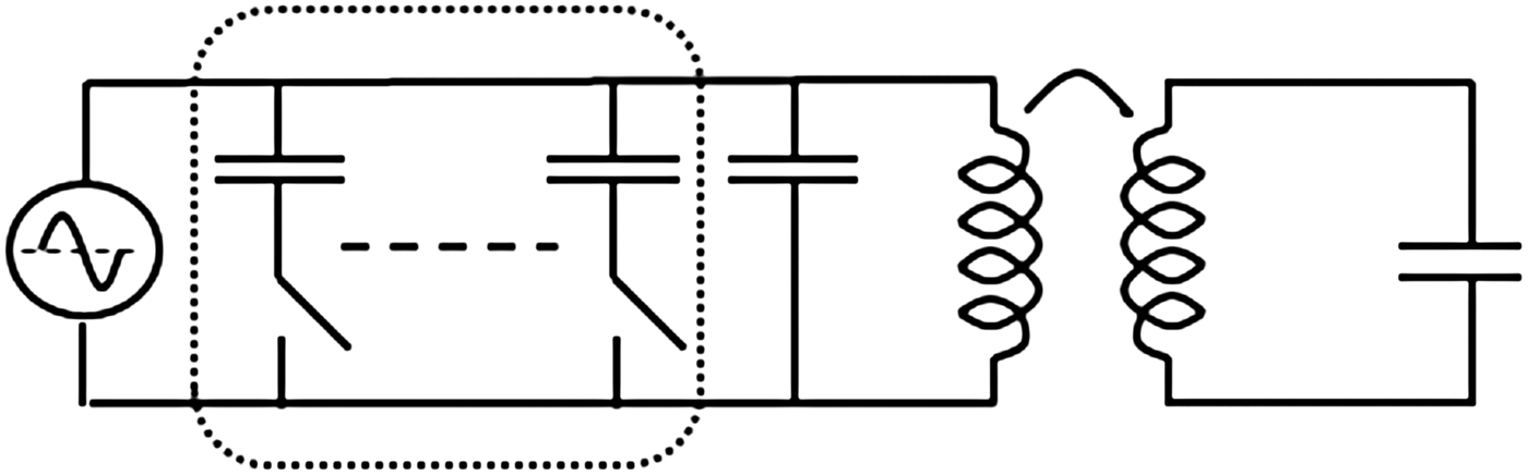
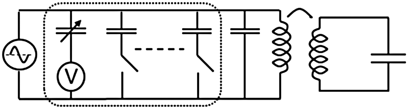
To provide dynamic tuning of the WPT system, different compensation techniques are used. Switchable capacitor arrays are proposed in [Reference Jung and Lee16, Reference Lee, Lim, Yang and Lim17, Reference Lee, Kwon, Li and Ghovanloo19] as shown in Fig. 4.
WPT system with switchable capacitor array (dotted-box).
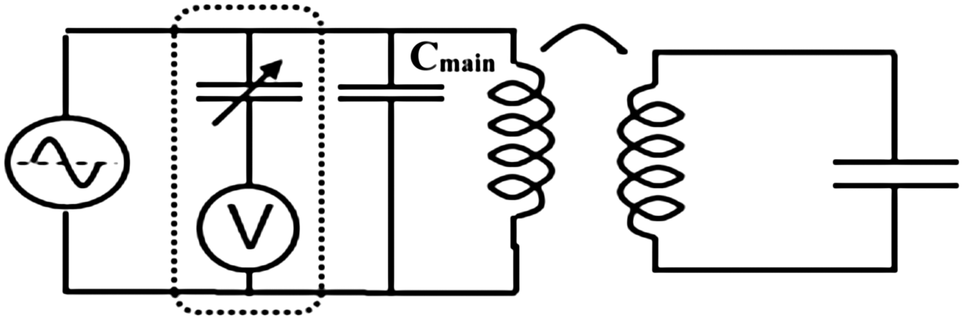
A diode-connected variable capacitor structure is used in [Reference Jung and Lee16, Reference Heebl, Thomas, Penno and Grbic18]. Here, Varactor structure based on a MOSCAP of Fig. 3 is utilized as shown in Fig. 5.
Varactor (dotted-box)-based WPT system.
In this circuit, C main is the main capacitor and it is directly connected to the primary self-inductor which plays a role in achieving high-Q value. Binary cap arrays or Varactors [Reference Buisman20, Reference Buisman, Cong, Zampardi and de Vreede21] will have lower-Q value compared with C main due to additional circuit components attached to them such as switches or DC bias voltages, etc.
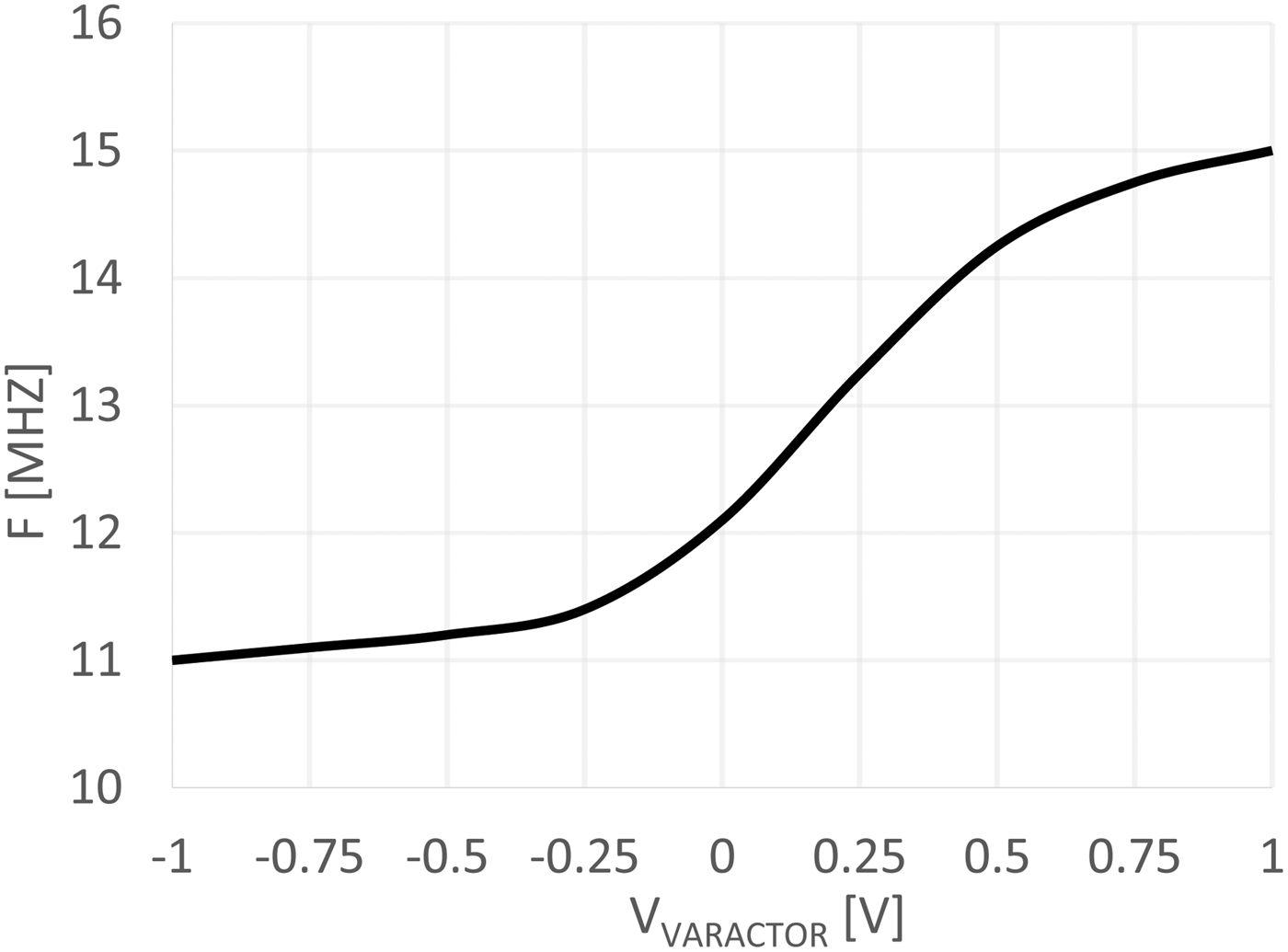
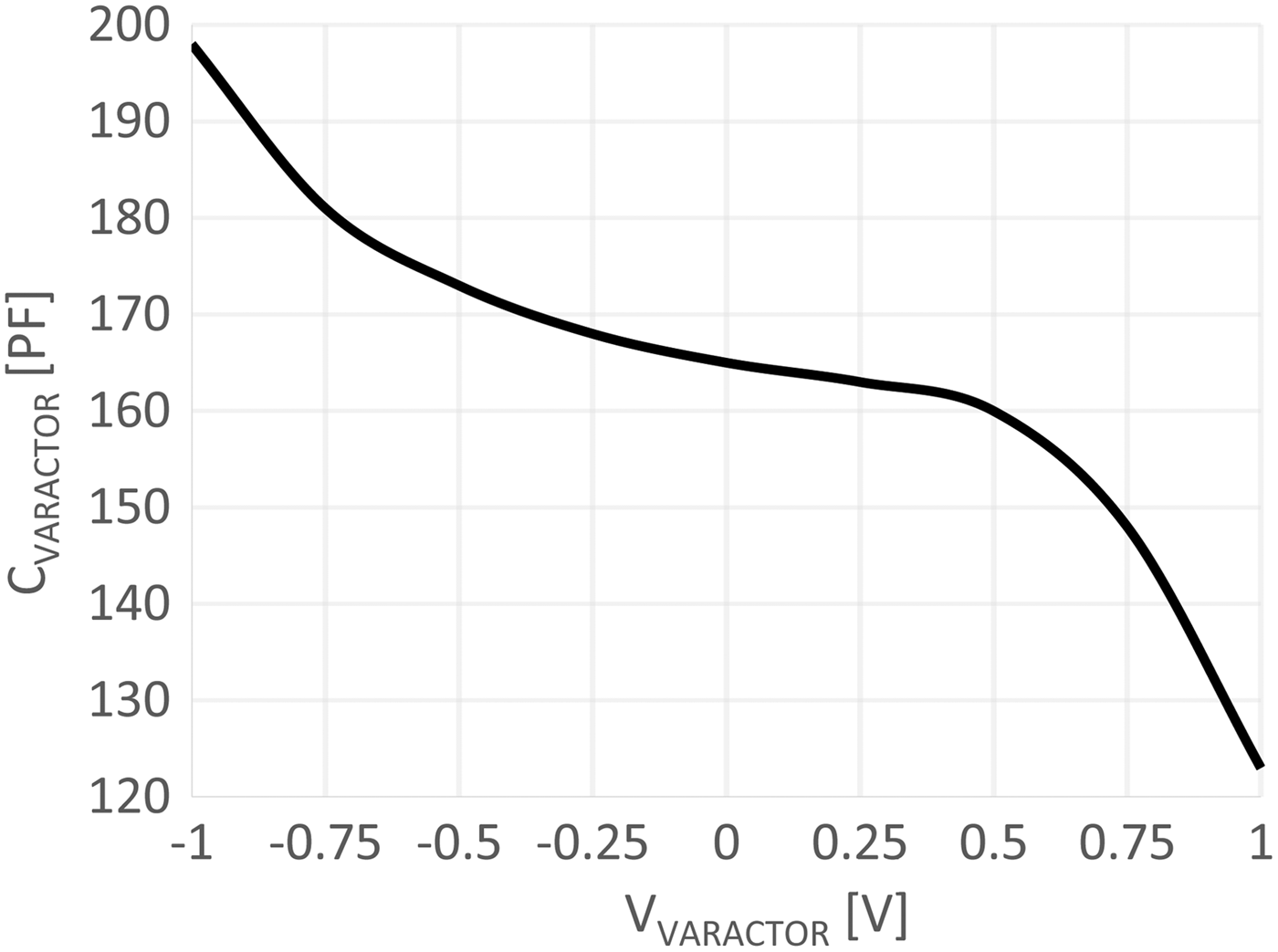
Tuning range of the Varactor in Cadence simulation results is shown in Fig. 6. The voltage bias (V) of the Varactor in the dotted box of Fig. 5 is varied from −1 to 1 V; hence, f resonance can be tuned accordingly from 11 to 14.9 MHz, where the target center frequency is 13.56 MHz. Figure 7 shows the range of MOSCAP from 120 to 200 pF when V is varied to tune the resonance frequency. This corresponds to tunability from −10% to +10% of nominal value the MOSCAP.
f resonance versus Varactor bias (V).
Capacitance of the MOSCAP (Varactor) versus Vbias.
At the same time, as seen in Fig. 6, the saturation happens when V is less than −0.5 V, or more than 0.7 V. Therefore, there is a need to increase tuning range using different architectures such as the hybrid capacitor structure shown in Fig. 8.
Hybrid resonance circuit (dotted-box) in WPT system.
The final proposed structure is shown in Fig. 8 where both Varactor and switchable cap arrays are used together for a hybrid model. In this model; while coarse tuning can be achieved by the Varactor section where V is changed to compensate for larger non-idealities of the resonance circuit, switchable capacitor array section can be used to provide fine tuning, so that smaller capacitors are used in the switchable capacitor array to minimize number of capacitors used.
Final total capacitor is equal to
 $${C_{total}} = {C_{main}} + {C_{switch}} + {C_{{\mathop{\rm var}} actor}}.$$
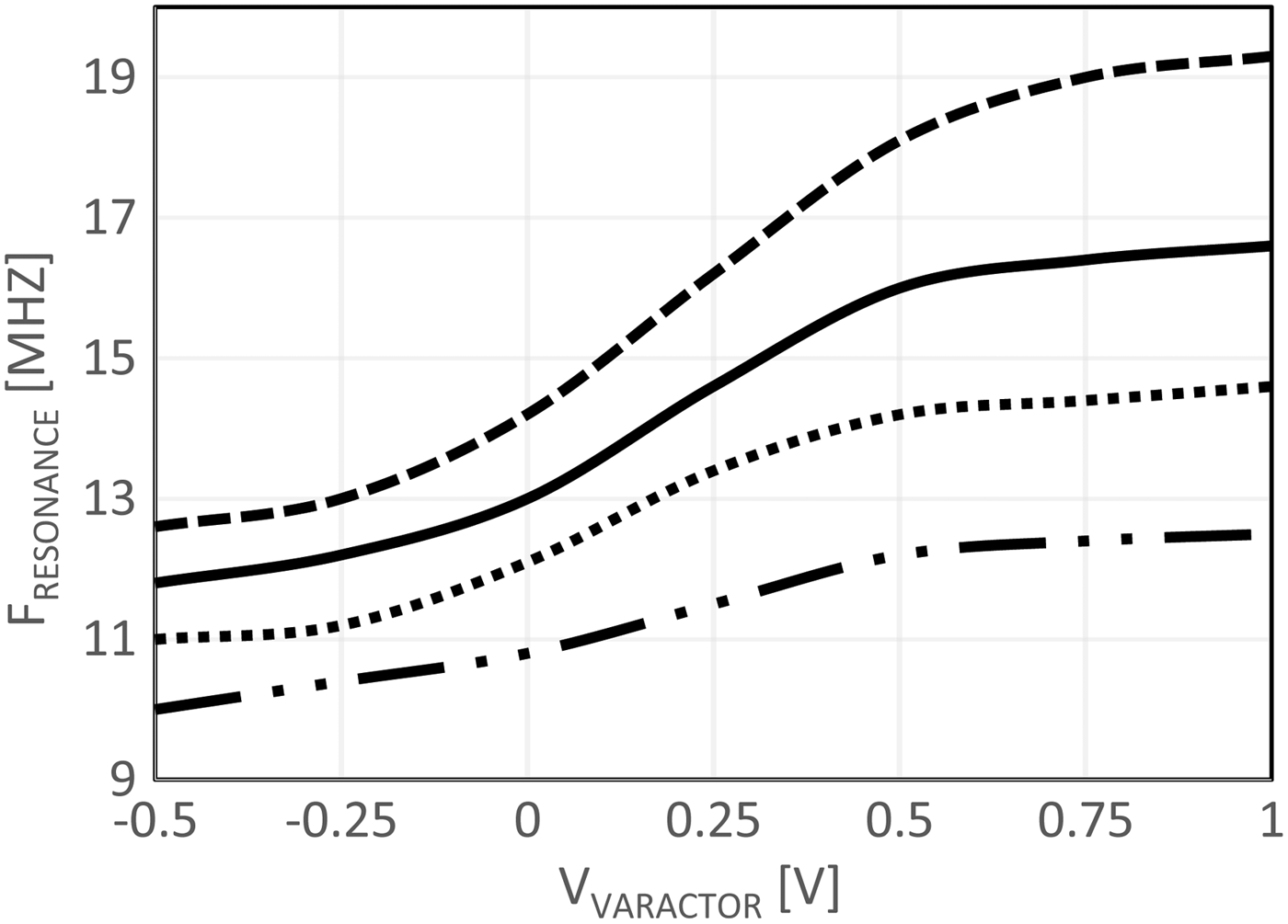
The hybrid architecture of Fig. 8 is simulated to show the extended range of tunability using both the switchable binary cap array as well as the Varactor. In this simulation, V of the Varactor is varied from −0.5 to 1 V and the switchable binary cap array is varied from 84 to 240 pF in four steps providing four separate curves in Fig. 9. The maximum frequency is increased up to 19.4 MHz (from 14.9 MHz of Fig. 6 when V = 1 V) and lower frequency is further pushed down to 10 MHz (from 11 MHz of Fig. 6V = −1 V). This will provide −/+35% of tunability range of the resonance frequency around 13.56 MHz.
Extended range of f resonance by varying both the binary cap array and the MOSCAP.
By using different options of binary cap array together with Varactor, all the values between upper and lower curves can be obtained. In Fig. 9, four different settings of binary cap array are used. As seen in Figs 6 and 9, tuning range by Varactor is a non-linear (not a straight-line) due to the nature of the MOSCAP. Using binary cap array provides finer steps, linear transitioning points, and extended range. Figure 10 shows the current signal transmitted from the transmitter antenna (I TX = 45 mApp) and current signal received at the receiver antenna (I RX = 5 mApp). Figure 11 shows voltage waveform at the transmitter antenna (V TX = 2 Vpp) and voltage waveform at the receiver antenna (V RX = 0.2 Vpp). At the same time, the resonant current through the Varactor is 20 mApp and the resonant current on the binary cap is 25 mApp. The power rating of the Varactor in this setup is 40 mW.
Transmitter and receiver current.
Transmitter and receiver voltage.
C) Detuning and simulation results
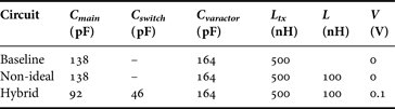
The values of circuit elements of the primary are shown in Table 1 for different schemes. As a baseline, an ideal case is considered where there are no losses in the circuit. To detune the circuit, an additional 100 nH is introduced for simulation purposes. This value represents about 20% deviation from the nominal antenna and chosen as an example. In reality, there will be so many detuning values possible due to varying distance and environmental effects between the transmitter and the receiver [Reference Dai and Ludois3, Reference Lu, Li, Ki, Tsui and Yue4].
Circuit element values of different primary structures.
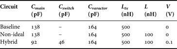
Different cap values are used to bring the circuit back to the resonant frequency. Figure 12 shows a simulation result where initially the primary (transmitter side of the system) is tuned to 13.56 MHz. After adding non-idealities in to the circuit, the transmitter power is deviated from the desired resonant peak to the left for the non-ideal case. The proposed hybrid structure is used to bring the resonant frequency back to 13.56 MHz, so that resonant peak of the transmitter aligns with that of the receiver.
Transmitted power of baseline (dashed), non-ideal (solid), and hybrid (dashed/dotted).
The received power signals of baseline, non-ideal and hybrid schemes in frequency domain when coupling coefficient (k) is equal to 0.1 is shown in Fig. 13. Received power is improved and it is only 0.12 dB away from the baseline when the power level is about −18 dB level.
Received power of baseline (dashed), non-ideal (solid), and Hybrid (solid with dots) when k = 0.1.
A different leakage inductance value (200 nH) is used for following simulations. In order to find the optimum value, both V (0.1–0.2 V) of the Varactor and also number (1–6) of binary capacitors are swept as seen in Fig. 14. It was observed that the largest received power is when V is equal to 200 mV and number of binary capacitors is 4, which is about 30 pF of binary cap value for this particular leakage inductance. With bigger leakage inductance, the received power by the proposed hybrid architecture is improved to more than 1 dB level as seen in Fig. 15.
Received power of Hybrid architecture when k = 0.1, L leakage = 200 nH versus V and number of binary cap.
Received power of Hybrid (k = 0.1, L leakage = 200 nH).
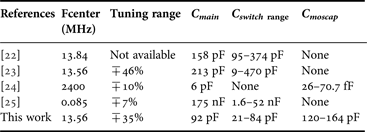
In Table 2, resonance tuning range and size of capacitors are compared [Reference Ogawa, Oodachi, Obayashi and Shoki22–Reference Saltanovs25]. It is noted that [Reference Sample, Waters, Wisdom and Smith23] tunes the system in both transmitter side as well as in the receiver side using the same size of capacitor array.
Comparison of capacitive tuning WPT systems.
V. CONCLUSION
Detuning of a WPT system is an important issue that affects overall power transfer efficiency. Dynamic tuning of these systems under various conditions is studied extensively in literature. In this paper, it is shown that Varactor and switch array capacitors can be used individually or together as a hybrid model to de-tune a WPT system. Varactor type has an advantage of saving layout area while switch array caps can provide fine tuning. Hybrid model can be used for the WPT applications in the MHz range to provide an optimum trade-off, where the quality is optimized using Cmain as a fixed capacitor. This architecture is successfully designed at 13.56 MHz. The tunability range of the resonance frequency is greatly extended around 13.56 MHz.