Scanning probes and the energy challenge
Meeting the energy needs of our maturing global civilization in an economically, environmentally, and geopolitically sustainable fashion is one of the most pressing technological challenges facing humanity today. We have heard the projections so often, sometimes we risk becoming complacent. Nevertheless, global energy consumption is on track to rise over 50% by 2035.1 Materials scientists have a critical role to play in meeting this challenge, and major research efforts are under way to develop new technologies with the potential to dramatically improve the way we transform, store, and use energy.
Scanning probe microscopy (SPM)Reference Bonnell2, Reference Meyer, Hug and Bennewitz3 is going to play a critical role in the search for new energy technologies for the reason that so many nascent energy technologies are based on nanostructured materials. For instance, organic solar cells require a large internal surface area that is currently achieved with a self-assembled nanostructured bulk heterojunction,Reference Groves, Reid and Ginger4 and nanoscale colloids are being used to fabricate inks for printing copper indium gallium selenideReference Guo, Ford, Hillhouse and Agrawal5 and copper zinc tin sulfide solar cells.Reference Guo, Ford, Yang, Walker, Stach, Hillhouse and Agrawal6 Quantum dots are also under intense study for use in potential solar cells,Reference Luque, Marti and Nozik7 and nanostructured electrodes are critical to efficient dye-sensitized solar cells.Reference Grätzel8 Strategies for energy harvesting based on artificial photosynthesis from biological or bio-inspired materials involve nanoscale control.Reference Davis, Morgan, Wrathmell, Axford, Zhao and Wang9
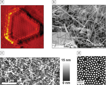
Nanostructured composites and superlattices are being studied as thermoelectric materials for converting waste heat to electricity,Reference Rao, Ji and Tritt10 and nanostructured catalysts are being developed for solar fuel generation,Reference Osterloh and Parkinson11 while metal nanostructures are being studied for enhancing light harvesting in both photovoltaic and photochemical energy conversion devices.Reference Atwater12 On the energy storage side, nanostructured electrodes are being used to increase capacity and improve stability of both batteriesReference Kim and Cho13 and super capacitors.Reference Simon and Gogotsi14 Nanostructured catalysts can be useful for the transformation of chemical products in a more energy efficient and environmentally friendly manner.Reference Haruta and Date15 SPM methods are making important contributions to energy-related materials technologies because of the unique opportunities that they offer to map nanoscale functionality such as surface potential, photoconductivity, catalytic activity, dielectric function, and even ion motion. The ability to image function on the nanoscale is being used to elucidate structure/function relationships in nanostructured materials for energy, often on working devices, and with exceptional resolution. Figure 1 illustrates a fraction of the wide variety of nanostructured materials currently being studied for energy applications, in which one might imagine using functional imaging to reveal local structure-function correlations.
Examples of the range of nanostructures that are currently being studied for use in solar cells, batteries, catalysts, thermoelectrics, and a host of other energy-related materials. (a) Scanning tunneling microscopy image of a MoS2 electrocatalyst on Au(111) (6 nm × 6 nm) (Reproduced with permission from Reference Reference Jaramillo, Jørgensen, Bonde, Nielsen, Horch and Chorkendorff41. ©2007, AAAS). (b) Scanning electron microscopy (SEM) image of a Si nanowire Li-ion battery anode (Reproduced with permission from Reference Reference Chan, Peng, Liu, McIlwrath, Zhang, Huggins and Cui42. ©2008, Nature Publishing Group). (c) Atomic force microscopy image of a nanowire organic solar cell (Reproduced with permission from Reference Reference Rice, Giridharagopal, Zheng, Ohuchi, Ginger and Luscombe43. ©2011, ACS). (d) An SEM image of electrochemically grown Bi2Te3–ySey nanowires of potential interest for thermoelectrics (Reproduced with permission from Reference Reference Martín-González, Snyder, Prieto, Gronsky, Sands and Stacy44. ©2003, ACS).

Scanning tunneling microscopy (STM) is the oldest technique in what is nowadays the broad field of SPM. Hence, after 25 years of routine application of atomic resolution STM, it is not surprising that properties determined from variants of STM have achieved high resolution as well. It is taken for granted that properties such as superconductor gap states and charge density waves can be mapped with atomic resolution. More surprising perhaps is the spatial resolution achieved while probing continuum properties. Resistance and capacitance can be mapped with 1–100 nanometer (nm) resolution,Reference Lanyi and Hruskovic16–Reference Freitag, Kalinin, Bonnell and Johnson18 while atomic and molecular resolution have been achieved for the work function and dielectric constant, respectively.Reference Bonnell19, Reference Brukman and Bonnell20
As highlighted by the examples on the following pages, recent advances apply these abilities to make measurements of complex properties in situations of relevance to energy devices. In situ SPM now probes device materials in the presence of both electric field and optical excitation, measures local electrochemistry in solution, and more.1, Reference Groves, Reid and Ginger4 For example, catalysis does not occur in a vacuum. New high pressure systems allow catalytic interactions to be probed under realistic environmental conditions, as described in the review by Besenbacher et al. Catalysis and electrochemistry can now be characterized in liquids, as summarized by Lai et al. Similarly, many photovoltaic devices involve the interaction of light with nanostructured materials to generate charge carriers, and O’Dea et al. review the many applications of SPM to understand both organic and inorganic thin-film photovoltaics. Lee et al. exploit local impedance probes to examine interactions in oxide fuel cells, lithium-ion batteries, and light harvesting proteins.
Not just surface topography
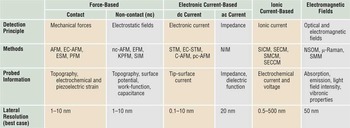
To a newcomer, the field of SPM can sometimes seem like a confusing alphabet soup of specialized techniques. The explosion of acronyms reflects the breadth and creativity of activity in this area. The precise control of the tip-surface junction became a platform for diverse property measurements. While it would be impossible to provide a comprehensive review of scanning probes in this issue, we try to provide the general reader with a high-level overview and some insight into the common vocabulary found in the feature articles that follow. Table I gives a concise summary of the popular techniques, many of which are featured in this issue of MRS Bulletin.
Overview of scanning probe microscopy-based techniques for probing functional properties.

AFM, Atomic force microscopy; EC-AFM, electrochemical atomic force microscopy; ESM, electrochemical strain microscopy; PFM, piezo force microscopy; EFM, electrostatic force microscopy; KPFM, Kelvin probe force microscopy; SIM, scanning impedance microscopy; STM, scanning tunneling microscopy; EC-STM, electrochemical scanning tunneling microscopy; C-AFM, conductive atomic force microscopy; pc-AFM, photoconductive atomic force microscopy; NIM, nanoimpedance microscopy; SICM, scanning ion-conductance microscopy; SECM, scanning electrochemical microscopy; SMCM, scanning micropipette contact method; SECCM, scanning electrochemical cell microscopy; NSOM, near-field scanning optical microscopy; SMM, near-field scanning microwave microscopy.
The invention of STM revolutionized (nano)science and founded the field of SPM.Reference Wiesendanger21 In brief, STM is based on the exponential distance dependence of the tunneling current between a conducting tip and sample. By laterally scanning the tip with respect to the sample, or vice versa, atomic resolution can be obtained in the tunneling current or in the height signal. In the former case, a feedback system is used to keep the tip-sample distance (tunneling current) constant. In scanning tunneling spectroscopy (STS), the feedback loop is briefly opened, enabling the local measurement of current-voltage characteristics.Reference Wiesendanger21
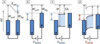
The field of SPM generalizes the approach of a tip-surface probe to an extensive range of interactions and, therefore, properties. In the following paragraphs, we give a brief introduction to scanning Kelvin probe microscopy (SKPM)Reference Nonnenmacher, O’Boyle and Wickramasinghe22 (also called Kelvin probe force microscopy [KPFM]) and electrostatic force microscopy (EFM),Reference Martin, Abraham and Wickramasinghe23, Reference Stern, Terris, Mamin and Rugar24 see also Figure 2. These techniques are two of the main workhorses for the local probing of functional properties and are intensively used for energy materials (see also the O’Dea et al. article). The more interested reader is referred to the extensive literature on this topic (e.g., Reference Reference Sadewasser and Glatzel25). The principle of SKPM and EFM is not unlike that of topographic atomic force microscopy (AFM) in the sense that an interaction force between the surface of interest and the apex of a sharp tip is probed in some way. The major difference is that AFM probes the surface topography via short range, Lennard-Jones-type potentials, whereas EFM and SKPM probe the surface potential via the Coulomb interaction.
Illustration of electrostatic force microscopy (EFM) and scanning Kelvin probe microscopy (SKPM). Dark blue rectangles indicate the metallic tip and sample (a–b) or substrate (c–d). The light blue regions in (c) and (d) indicate a semiconductor. The electrostatic force between the tip and sample is probed in EFM (a); nullification of this force in SKPM (b) enables quantitative surface potential measurements, which may be complicated by the presence of a semiconductor (c), causing interfacial dipoles or space charges (d). E vac, electric field in a vacuum; W surf, work function of sample surface; W tip, work function of tip; V SKPM, compensating bias in SKPM; IP, ionization potential; and EA, electron affinity.

Due to the long-range nature of the Coulomb force, truly “local” measurements in SKPM and EFM are challenging; nevertheless, atomic resolution has been obtained with SKPM, although this is the subject of some controversy.Reference Kitamura, Suzukia, Iwatsukia and Mooney26, Reference Enevoldsen, Glatzel, Christensen, Lauritsen and Besenbacher27 Like in AFM, EFM and SKPM signals can be extracted from either the interaction force itself or from the force gradient. Although these signals could, in principle, be probed in dc mode (cf. contact mode AFM), EFM and SKPM are always performed in ac (non-contact) mode, in which the tip oscillates with respect to the sample, as this gives a superior signal-to-noise ratio. For both techniques, an ac bias with frequency ω is applied to the tip or sample. Treating the tip as a simple harmonic oscillator, it is easy to derive that the Coulomb force between the tip and sample is proportional to dC/dz, with C being the tip-sample capacitance and z the tip-sample distance, and gives rise to tip oscillations at ω and 2ω. Similarly, the force gradient is proportional to d2C/dz 2 and causes an oscillating shift of the tip’s resonance frequency.Reference Sadewasser and Glatzel25 Since capacitance scales in the lowest order as C α 1/z, it follows that force gradient detection is least susceptible to (undesired) couplings between the sample and parts of the tip other than its apex. Hence, force gradient detection typically shows superior spatial resolution. By working at one of the cantilever resonances, detection is usually more sensitive.
The working principle of EFM and SKPM is explained in Figure 2. When two metals with different work functions W are connected (Figure 2a), an electric field (shown as a gradient in the vacuum level E vac) is created and exerts a force (and force gradient) on the tip. In SKPM, this force is nullified by applying a compensating bias V SKPM via a feedback system (Figure 2b); in EFM, this feedback is absent, and the force (gradient) itself is mapped. In the situation of Figure 2b, SKPM probes the work function difference W surf –W tip between the tip and the sample surface. Insertion of an ideal intrinsic semiconductor (characterized by its ionization potential IP and electron affinity EA) between the tip and sample (Figure 2c) has no effect on the SKPM signal. In the case in which an interfacial dipole layer exists between the substrate and semiconductor or when the semiconductor contains bulk uncompensated charges (Figure 2d), the SKPM signal changes: by nullifying the force on the tip, the feedback nullifies the electric field at the tip. Generally, SKPM probes the electrostatic potential of the sample and, in special cases (Figure 2b–c), statements about the sample work function or Fermi level can be made.
Probing more complex properties
SPM-based methods that probe dynamic material responses sometimes require multi-frequency excitation and detection. These methods include approaches to accessing piezoelectric and ferroelectric interactions, dielectric function, and ionic motion. Such properties are critical to several energy storage and conversion strategies.
One technique, important for piezoelectric materials used for information storage and energy harvesting, is piezoresponse force microscopy (PFM).Reference Gruverman, Auciello and Tokumoto28 PFM probes the electromechanical material response (i.e., a change in strain in response to an electronic stimulus). Here, a single frequency ac bias, V ac, is applied to a conductive SPM tip in contact with the sample surface. As a consequence of the piezoelectric effect, described by a linear relationship between the strain, S, and electric field, E, with the piezoelectric coefficient, d, as a proportionality constant, a change in strain is induced by the electric field. The dynamic strain change in response to the applied V ac can be detected as a surface oscillation with the same tip used to apply the electric field. Using lock-in techniques, the amplitude and phase of the sample response can be extracted, and information about the local piezoelectric strength and domain orientation can be mapped. In addition to domain imaging, PFM can be used to manipulate the domain orientation by applying a dc bias, V dc. Applications of domain manipulation include domain poling and measurements of local piezoelectric hysteresis. PFM has been widely used on various materials such as ceramics,Reference Buscaglia, Buscaglia, Viviani, Petzelt, Savinov, Mitoseriu, Testino, Nanni, Harnegea, Zhao and Nygren29 thin films,Reference Gruverman, Auciello, Ramesh and Tokumoto30 polymers,Reference Noda, Ishida, Kubono, Horiuchi, Yamada and Matsushige31, Reference Rodriguez, Jesse, Kalinin, Kim, Ducharme and Fridkin32 and biological samplesReference Kalinin, Rodriguez, Jesse, Thundat and Gruverman33 and has become a standard characterization technique that is commercially available.
A recent advancement of PFM is high-frequency PFM, where the contact resonance peak of the tip-sample system is utilized to achieve 100 times higher signal/noise ratios compared to off-resonance PFM. With this development came the need for multiple frequency excitation and detection because of ambiguities associated with the dependence of the contact resonance frequency on sample roughness and tip state that results in falsified information when single frequency methods are used. Currently, multiple frequency techniques are realized through dual ac resonance trackingReference Rodriguez, Callahan, Kalinin and Proksch34 and band excitation,Reference Jesse, Kalinin, Proksch, Baddorf and Rodriguez35 described in the article by Jesse et al. in this issue of MRS Bulletin. The use of multiple frequency techniques is not limited to PFM but can be applied to other non-contact SPM techniques as well.
The concept of PFM (i.e., the characterization of electromechanical sample properties) is not exclusively used for piezoelectric materials but can be applied to every sample system where a strain change can be induced by bias. This concept led to the development of electrochemical strain microscopy (ESM) for energy storage materials, including Li-ion batteriesReference Balke, Jesse, Kim, Adamczyk, Tselev, Ivanov, Dudney and Kalinin36, Reference Balke, Jesse, Morozovska, Eliseev, Chung, Kim, Adamczyk, Garcia, Dudney and Kalinin37 and solid oxide fuel cells.Reference Kumar, Ciucci, Morozovska, Kalinin and Jesse38 Here, the locally applied bias changes the local ion concentration (Li+ or O2‒), which results in a change in sample volume. For Li-ion battery materials, this can be up to 400% for Si anodes. With the development of ESM, it is possible to investigate the local ionic transport on relevant lengths scales of single microstructural elements down to 10 nm, which was not possible before.
Polarization is a complex property represented by the dielectric constant κ, which plays a major role in many materials in energy generation and storage systems. Dielectric polarization is inherent in the interaction of light with solids, the motion of ions in ionic materials, electrical charges trapped at interfaces, and dipoles in organic and biomolecules. Recent strategies to locally probe dielectric function involve light scattering from a tip-surface junction,Reference Nikiforov, Schneider, Park, Milde, Zerweck, Loppacher, Eng, Therien, Engheta and Bonnell39 second harmonic capacitance gradient detection in EFM, and scanning impedance microscopy and its variants.Reference Shao, Kalinin and Bonnell40 Impedance is defined as the (complex) ratio of a periodically varying applied voltage to the resulting current and is measured as a function of frequency. The combination of impedance with SPM allows the real and imaginary components of the dielectric function to be accessed with high spatial resolution. Fundamental processes such as charge trapping-relaxation, ion diffusion, and molecular dipole reorientation occur at different time scales which, in principle, can be distinguished with scanning impedance probes. In the article by Lee et al., applications in Nafion, as a proton exchange membrane for fuel cells, Li battery-based materials, and energy harvesting protein systems, are explored.
Future opportunities
The first generation of scanning probe microscopy (SPM) techniques—scanning tunneling microscopy, atomic force microscopy, and electrostatic and magnetic force microscopies—are now considered essential tools in materials characterization and are used routinely in basic and applied research as well as industry-based development. However, the potential of the second and third generation techniques may not be well known, partially due to the fact that the most advanced techniques are not yet available commercially. When they are commercially available, for example, as in the case of KPFM, they have a tremendous impact. As the articles in this issue illustrate, the solutions to our energy challenges demand the characterization of local functional properties. We hope that the reviews in this issue will inspire and enable many to exploit these tools in energy research.
From the perspective of fundamental research of SPM itself, it is an exciting time. Rather than standing on a maturity plateau after the first two decades, we are poised at the beginning of a new generation in SPM technology as we push the spatial resolution of functional probes to higher levels. These advances will in turn propel our fundamental understanding of energy-related materials and enable solutions to some of our most important energy challenges.
Acknowledgments
D.B. is grateful for support from the DoE Office of Basic Energy Science, Division of Materials Science DE-FG02-00ER45813, and the National Science Foundation NSEC DMR08-32802.