Introduction
Ultrafast lasers, which are pulsed lasers with pulse duration in the femtosecond (fs) or picosecond (ps) range, have gained wide acceptance over the past several years as a unique tool for advanced high-precision manufacturing. The ultrashort pulse duration and the high intensity on the target lead to complete ionization of the irradiated volume by nonlinear effects. Since the pulse duration is less than the heat diffusion time, the irradiated volume is ejected before any heat diffusion or thermal damage can take place, and consequently, side effects are significantly reduced as compared to longer pulses. The decreased side effects result in preserving the functionalities of the material and enable fine and accurate microfabrication processes such as drilling, cutting, engraving, and internal marking.
However, because of the non-thermal nature of the ablation process, the quantity of matter removed per laser pulse is relatively small, and many technology developments have taken place to ensure that the overall industrial process reaches a productivity scale sufficient for economic use. In particular, three fields have been key to the current development of industrial laser applications: Laser technology, ultrafast laser–matter interactions, and beam handling and delivery.
The average power of the laser is key for high-throughput industrial use. The first generation of ultrafast lasers, introduced in the early 2000s, had an average power of 1 W. Today, multiple technologies allow average laser power levels to reach between 100 W for industrial lasers and more than 1 kW in scientific proofs-of-principle experiments. Reference Eidam, Hanf, Seise, Andersen, Gabler, Wirth, Schreiber, Limpert and Tünnermann1–Reference Russbueldt, Mans, Weitenberg, Hoffmann and Poprawe3 The key feature is the capacity of the laser medium to dissipate the heat generated while under high-average-power operation.
Fiber lasers allow a high average power to be easily reached by distributing the heat along the fiber length. However, specific fiber geometries such as microstructured photonic crystal fibers are required to offer an energy per pulse sufficient for industrial applications. Reference Eidam, Hanf, Seise, Andersen, Gabler, Wirth, Schreiber, Limpert and Tünnermann1 On the other hand, thin disk lasers (i.e., lasers using a thin laser crystal as the active material for efficient heat dissipation) can provide both high energy and high average power, but the laser repetition rate is usually limited to a few hundred kHz. Reference Negel, Loescher, Voss, Bauer, Sutter, Killi, Ahmed and Graf2 Other approaches, such as the use of multipass slab geometries, also show significant potential. Reference Russbueldt, Mans, Weitenberg, Hoffmann and Poprawe3 Today, industrial lasers with power in the range of 100 W are commercially available from several manufacturers, with most of them operating with moderate pulse energies (typically <300 µJ) and high repetition rates (up to several MHz).
Yet, the average power of the laser alone is not sufficient to guarantee industrial productivity. Although the nature of the laser–matter interaction is virtually athermal in the sub-ps domain, heat accumulation occurs when the laser is operated at a high repetition rate, which can be detrimental to the process quality. High-speed beam handling becomes of paramount importance to maintain the quality of the process at high speeds.
In this article, we present two particularly elegant industrial solutions to this requirement: the use of diffractive optics for high-speed drilling of inkjet nozzles and hybrid high-speed scanners for applications in electronics packaging.
In addition, the non-thermal, ultrafast laser ablation regime has enabled the development of new industrial processes. In particular, the field of surface functionalization is especially active, as ultrafast laser processing has the potential to offer micro- or nanoscale surface structuring. We present two examples of battery optimization and semiconductor nanotexturing.
High-speed parallel drilling of inkjet nozzles
Today’s color inkjet printers are a widely used consumer and commercial product, with large annual sales and revenue for many companies. One of the key components of the inkjet printer is the inkjet nozzle plate. The inkjet nozzle plate is a thin foil containing hundreds to thousands of small holes, through which microscopic droplets of ink are ejected onto the paper to form text and graphics. These holes are designed to exacting specifications and uniformity to ensure the high printing quality expected from today’s inkjet printers. A high-precision manufacturing process based on ps laser ablation has been successfully developed for the production of inkjet nozzle plates. Reference Liu4
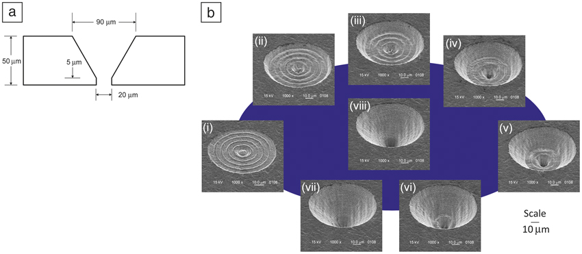
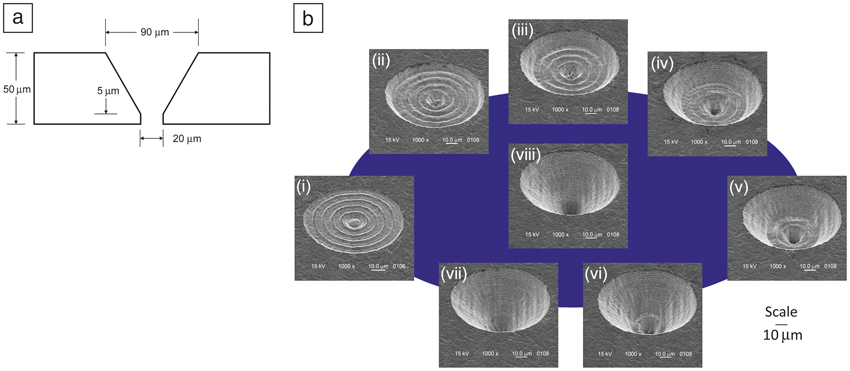
The inkjet nozzle geometry design is shown in Figure 1a. A drilling method called laser milling was developed to drill holes with adjustable tapered profiles, as shown in Figure 1b. A thin layer of material of thickness, Δh, is ablated by moving the laser spot in a spiral on the workpiece surface. The outer diameter of the spiral defines the diameter of the layer removed. A second layer is again ablated, but with the outer diameter D of the spiral reduced by an amount equal to ΔD = 2Δhtanα, where α is the desired taper half angle. This process is repeated a number of times until the desired depth is reached. By controlling the depth of each layer removed and the outer diameter reduction between successive spirals, the amount of taper of the milled hole can be precisely adjusted. The laser spot size used for milling the inkjet nozzle hole in Figure 1b had a diameter of 10 μm. After milling the tapered portion of the nozzle, the 20-μm-dia. straight exit hole was machined with trepanning, where the focused laser spot simply traced a circle a number of times (image viii in Figure 1b). Reference Liu4
(a) Geometry of inkjet nozzle hole in 50-μm-thick stainless-steel foil. (b) The laser milling process to drill holes with precise taper control. The process starts at the scanning electron microscope picture (i) and finishes at picture (viii). Reference Liu4
The laser milling development work showed that the best ablation results were obtained for relatively low laser fluences on the workpiece, approximately 1 J/cm2. With a 10-μm spot size, this translates 1 μJ/pulse. At this pulse energy level, a single inkjet nozzle hole takes more than one minute to finish. If the holes were drilled one at a time, the production cost would clearly be prohibitively high. On the other hand, the laser used produced 1 mJ/pulse at 1 kHz for an average power of 1 W, and if we had to drill one hole at a time, we would have wasted more than 99% of the available pulse energy.
The solution to this dilemma is parallel processing, using a custom-designed and fabricated phase-only diffractive optical element (DOE) as a “lossless” beam splitter. Reference Herzig5 Besides the obvious advantage of having a high-transmission efficiency, a DOE beam splitter is compact and easy to align as it is translationally invariant. Hundreds or even thousands of beams emerging from a single incident beam can be generated. The DOE splits beams into different angles of propagation.
To generate the desired inkjet nozzle pattern in a transverse plane, a custom f-θ telecentric scan lens of focal length f converts the angle θ of each beam emanating from the DOE beam splitter into a transverse location f × θ in the focal plane of the scan lens. The telecentricity of the scan lens makes all beams incident upon the workpiece normal to the workpiece, which is important to inkjet nozzle hole drilling. To generate a two-dimensional (2D) inkjet nozzle pattern, a 2D DOE with high efficiency and uniformity was designed and fabricated. Depending on the particular inkjet nozzle pattern, up to 400 beams were generated by the DOE. Reference Liu4
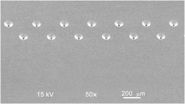
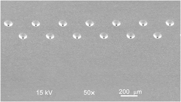
The final key element of the drilling system is an optical scanner to carry out the laser milling algorithm. Because each beam’s scan range was small—it only had to scan over a range of less than 90 μm—a high-resolution 2D piezo scan mirror was the best choice. A computer program was developed to implement the laser milling algorithm to drive the piezo scan mirror. Figure 2 shows the inkjet nozzle holes made by the process. Reference Liu4
Portion of inkjet nozzle plate made by parallel drilling with a diffractive optical element beam splitter, a piezo scan mirror, and a scan lens. Reference Liu4
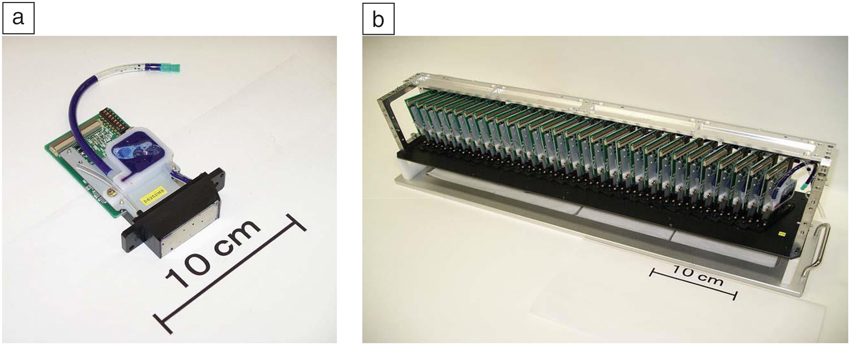
The ps laser drilling process and the system we describe are cost-competitive with other manufacturing methods. The system has been adopted for production use in a factory. Figure 3 shows the assembled inkjet head containing a nozzle plate, and the assembled line head with multiple inkjet heads that span the width of the print paper for high-speed industrial printing at a printing speed of 60 m/min. Reference Liu4
Inkjet printer components manufactured by picosecond (ps) laser processing. (a) Inkjet head with inkjet nozzle plate; the ps laser-drilled nozzle holes are in the front stainless-steel plate. (b) Assembled inkjet line head with multiple inkjet heads. Reference Liu4

High-speed ultrafast laser processing for electronic packaging
As consumer devices grow in functionalities and shrink in size, miniaturization of components and packaging have become the best opportunities for manufacturers to reduce cost and differentiate. Laser systems have been widely used for electronics packaging for decades due to their advantages in quality, speed, and capability to handle small features and brittle materials. As ultrafast laser technology matures, these new sources are playing increasingly important roles in the packaging industry for applications such as hole drilling, scribing/scoring, and cutting.
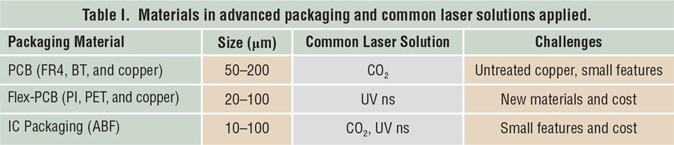
For example, VIAs (vertical interconnect accesses) are small holes drilled in electronic packaging materials to establish electrical connections in multilayer circuits. Table I summarizes some of the popular packaging materials, VIA size range, and the most commonly applied lasers. 6
Materials in advanced packaging and common laser solutions applied.
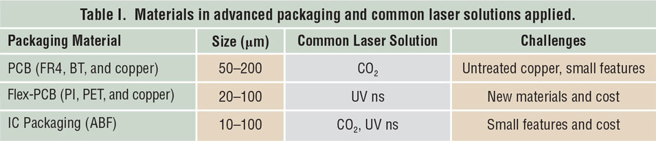
Note: PCB, printed circuit board; FR4, fire-retardant glass-reinforced expoxy laminate sheets used in PCB industry; BT, reinforced PCB substrates with bismaleimide-triazine resins; PI, polyimide; PET, poly(ethylene terephthalate); IC, integrated circuit; ABF, Ajinomoto buildup film; UV, ultraviolet; ns, nanosecond. 6
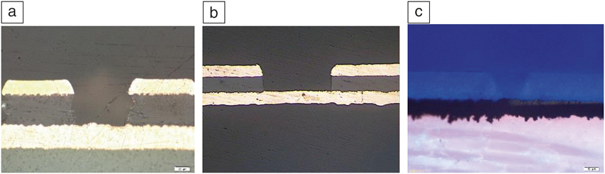
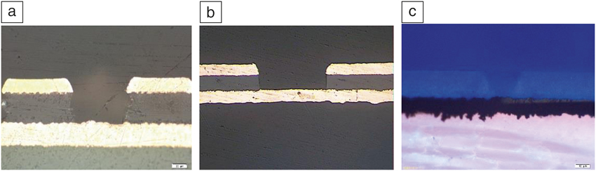
As VIA diameters shrink and new materials emerge, these traditional solutions start to face challenges of resolution, cost, and quality. For example, CO2 lasers become less capable at effectively removing untreated copper and for drilling features smaller than 40 µm in size. UV (ultraviolet) lasers are not efficient at processing some new materials (due to lack of absorption) and can introduce cost challenges. In contrast, ultrafast lasers have been shown to overcome the barriers of nonabsorption, multilayer stacks, and thermal damage, making them ideal alternatives for high-quality small features in electronics packaging applications. Reference Finn, Lin, Kleinert, Darwin and Zhang7 Figure 4 illustrates VIAs drilled in copper-clad printed circuit board (FR4), copper-clad polyimide, and solder-resist film, by using laser sources in the ps to fs regime. Reference Zhang8,Reference Zhang9 Benefiting from the high peak power, nonlinear absorption, and small achievable spot size, these ultrafast solutions offer advantages of minimal heat-affected zone, superior hole taper and sidewall quality, and small VIA capabilities that exceed the limits of their predecessors. Reference Chichkov, Momma, Nolte, Von Alvensleben and Tünnermann10
High-quality vertical interconnect access drilled with ultrafast lasers in (a) a printed circuit board (50-μm-top dia.), (b) copper-polyimide (50 μm), and (c) solder-resist film (25 μm).
As an industrial application, however, quality and capability benefits alone are not sufficient to trigger market adoption. Enabling high-process throughput and low average cost per feature (cost of ownership) are key to commercial success. The availability of high average power ultrafast lasers enables throughput scaling with lower potential cost and higher quality. The challenge is to apply such high power (greater than 50 W) while retaining the benefits of ultrafast laser–material interactions. In general, a sufficiently low pulse overlap (overlap of the laser spot diameter compared to the distance between adjacent laser pulses) of <50% is key to maintain high quality and avoid unfavorable effects such as heat accumulation, stress buildup, and plasma/plume shielding. Reference Bechtold, Hohenstein and Schmidt11
For traditional scanning equipment such as stages, rotary optics, and galvanometers, system acceleration (inertia related) and servo gain bandwidth (how fast in terms of frequency a system can respond to a command) pose strong limits in maximum beam scan speeds for next-generation features with decreasing sizes. As an example, a galvanometer with 2 kHz bandwidth is limited to approximately 30 kHz lasers while drilling a 50-µm-dia. hole with a 20-µm spot, under the 50% pulse overlap guideline. This restricts the selection of lasers and the maximum average power applicable, which counteracts the cost advantage brought by new laser developments at high repetition rates.
Inertialess scanners, such as acoustic optic (AOD) and electric optic deflectors, provide much higher bandwidth to enable laser processing at tens of MHz level under the same pulse overlap, but are limited by small scan fields (a few tens of laser spots) and are not suitable for large panel (> 500 × 600 mm) processing.
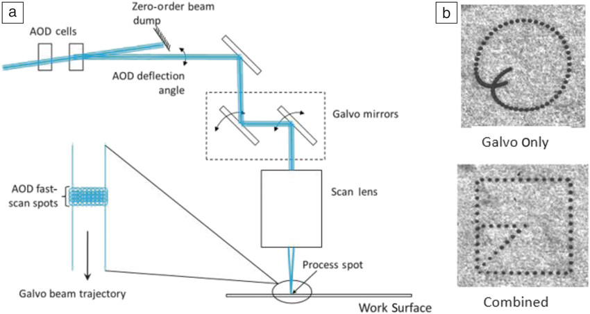
Recent system developments combine stages, galvanometers, and AODs into a coordinated tertiary architecture for high-bandwidth and large-field beam positioning. Reference Cutler, Pailthorp, Unrath, Richardson and Cable12 Figure 5 illustrates a schematic of such a beam-positioning technology. Two AODs are placed ahead of the galvanometers to enable rapid X/Y laser placement through the scan lens. In addition, the workpiece moves with 3D stages for long-stride low-frequency travel. Synchronized movements of these three component levels allow extremely fast local laser-beam speed and continuous motion over the entire range of stage travel. Benefiting from the wide bandwidth of the AOD scanners, this system can support up to a 15 MHz laser under similar conditions of 20 µm spot, 50% overlap. Furthermore, it enables up to 3 MHz pulse-to-pulse random access within the AOD field, which means the move time between subsequent laser spots can be as low as ∼300 ns compared to the ∼300 µs limit by galvanometers. This fast scanning speed greatly improves the system throughput and allows high-quality low-cost ultrafast machining with emerging high average power laser sources.
(a) A tertiary beam positioning system enabling extremely high-speed beam scan and high-power ultrafast laser processing. (b) 600 µm × 600 µm square pattern scanned at 5 m/s linear speed (top) with a galvanometer with 2 kHz bandwidth and (bottom) tertiary acoustic optical deflector (AOD) scanner with 1 MHz bandwidth. Reference Zhang8,Reference Zhang9

In addition to the high-speed beam manipulation, AODs also provide pulse-by-pulse energy control and fast rastering, which allows real-time width and depth control in the laser patterning, scribing, and dicing applications. Reference Zhang, Yang, Unrath and Orrick13 Combining the high-quality and flexible control, AOD-based tertiary laser scanning systems extend ultrafast machining to the high-megahertz domain, reaping the benefits of the shorter pulses, growing laser power, and ever-reducing photon cost.
Nanostructuring of silicon surfaces
Ultrafast laser-induced nanostructuring with the possibility of simultaneously modifying material properties has great potential to enable novel photonic applications. Reference Gattass and Mazur14 More specifically, ultrafast laser-induced nanostructuring of silicon (Si), which is by far the most widely used semiconductor with applications ranging from electronics to solar cells, can potentially be rewarding.
Ultrafast laser-induced periodic and quasiperiodic micro/nanostructures are perhaps among the most fascinating in terms of interactions with light. Reference Bonse, Krüger, Höhm and Rosenfeld15,Reference Vorobyev and Guo16 Two types of surface structures can be formed, depending on the laser wavelength (spatial size of the structures compared to the laser wavelength)—laser-induced periodic surface structures with low (coarse) and high (fine) spatial frequency features, depending on the pulse condition. The underlying physical formation mechanism of these structures is not yet fully understood.
There are two existing theories: (1) classical approach where pattern formation is explained by a spatially modulated energy deposition (“interference” pattern) theory; and (2) self-organization due to the ultrafast laser-induced instability at the surface and subsequent relaxation. Reference Vorobyev and Guo16 The classical approach is particularly insufficient to explain the formation of nanostructures much smaller than the laser wavelength. It should be noted that there is a great degree of freedom in tailoring different geometrical features of these structures. The most influential parameters are laser-pulse characteristics, energy, polarization, laser fluence, number of laser shots, and ambient pressure. Fs laser processing has been used to trigger the formation of Si micro/nanospikes. Reference Her, Finlay, Wu, Deliwala and Mazur17,Reference Shen, Carey, Crouch, Kandyla, Stone and Mazur18
Figure 6a shows a schematic of different nanostructure formation processes on the surface of Si. The evolving patterns from nanoripples to nanobeads to spikes are formed by changing process parameters. Reference Sarnet, Carey and Mazur19 Small laser-induced periodic structures are created on the surface after the first laser shots (Figure 6a[i]). These structures (Figure 6a[ii–iv]) transform into larger and more hydrodynamically stable beads (Figure 6a[v]) by applying higher energy densities and number of pulses. Due to the nonuniform absorption of laser light on the beads, they evolve into conical structures and spikes by continuing the process (Figure 6a[v–vii]).
Black silicon and its optical properties. (a) Schematic of formation process of different femtosecond (fs) laser-induced micro/nanostructures on Si by changing the laser-pulse characteristics (steps i–vii): Reference Sarnet, Carey and Mazur19 (i) Initiation of laser-induced periodic structures on the surface after the first laser shots. (ii–iv) Transformation process of laser-induced structures into larger beads (v) by applying higher energy densities and number of pulses. (v–vii) Evolving process of beads into conical structures and spikes due to the nonuniform absorption of laser light on the beads. (b) Scanning electron microscope image showing the surface morphology of black silicon, which corresponds to (vii) in (a), obtained by fs laser processing. (c) The absorption of fs laser processed Si (black Si) in the presence of different heavy chalcogens (sulfur [S], selenium [Se], tellurium [Te]) increased dramatically both below and above the bandgap, compared to that of crystalline Si. Reference Franta, Sher, Lin, Phillips and Mazur21 Note: IR, infrared; fs, femtosecond.

In addition to micro/nanostructuring, it is possible to simultaneously modify certain material properties with ultrafast lasers. Mazur and colleagues at Harvard University demonstrated that quasi-periodic micro/nanospikes (Figure 6b) with a thin doped layer at nonequilibrium levels could be obtained using fs-laser processing of Si in the presence of heavy chalcogens (e.g., S, Se, or Te). The optical hyperdoping process creates a “black silicon” surface with high and broadband absorption, in the visible and infrared. Reference Her, Finlay, Wu, Deliwala and Mazur17,Reference Sher, Winkler and Mazur20 The high absorption in black Si is attributed to both suppression of reflectance (due to geometrical effects) and doping (Figure 6c). Reference Franta, Sher, Lin, Phillips and Mazur21
Black silicon can be used to make high-sensitivity, Si-based photodiodes that perform well in both the visible and near-infrared regimes, where its performance approaches that of InGaAs. The fs-processed Si detectors show high gain and response at photon energies as low as 0.8 eV, which is a great improvement compared to that of standard Si photodetectors (1.1 eV). Reference Huang, Carey, Liu, Guo, Mazur and Campbell22
One should note that the two fs laser-induced processes, nanostructuring and doping, can be decoupled. Reference Lin, Mangan, Marbach, Schneider, Deng, Zhou, Brenner and Mazur23 Generally, increasing dopant concentration beyond the saturation limit is a challenging task. However, it has tremendous potential for improving the functionality of many devices. For example, many wide-bandgap semiconductors have low solid solubility and large ionization energies for at least one type of dopant. Reference Luo, Zhang and Wei24 Therefore, optical hyperdoping using fs lasers is an interesting and rewarding research topic by itself.
Ultrafast laser micro/nanostructuring of thick-film battery electrodes
For mobile applications as well as for electrical vehicles, lithium-ion batteries (LIBs) are essential for providing electrical energy. Reference Goodenough and Kim25–Reference Amatucci, Pasquier, Blyr, Zheng and Tarascon27 Thick-film electrodes, anodes, and cathodes in modern lithium-ion cells are complex multimaterial systems with defined material components, grain sizes, and porosities. State-of-the-art batteries with pouch cell geometry for high-power applications consist of up to 100 layers made of anode sheets, separator membranes, and cathode sheets that are stacked for achieving capacities of up to 40–60 Ah. The electrode materials with typical film thicknesses of approximately 50 µm are deposited (e.g., by tape casting) on 10–20-µm-thick aluminum (cathode) or copper (anode) current collectors. The footprint area of 52 Ah pouch cells can reach values on the order of 21 × 24 cm2. Reference Wood, Li and Daniel28
On the material level, commercial LIB can reach gravimetric energy densities of up to 600–700 Wh/kg. Due to the fact that a complete cell also consists of inactive materials such as metallic current collectors, separators, electrolyte, binder, and carbon black, gravimetric energy density on the cell level drops to values <150 Wh/kg. As calculated in Reference Reference Wood, Li and Daniel28, the total weight of a 52 Ah LIB in the pouch cell design is 1140 g, while the weight of the active material (lithium nickel manganese cobalt oxide [NMC]) is only 347 g. It is now an engineering challenge to reduce the gap between cell and material level. An increase in the cathode film thickness from 50 µm to 150 µm or 300 µm would lead to an increase in specific cell capacity of 22% or 30%, respectively, which is due to fewer inactive components (copper, aluminum, and separator) being required per cell. For example, a standard 52 Ah cell consists of 36 double-side coated anodes, two single-side coated anodes, 37 double-side coated cathodes (film thickness for each cathode sheet: 50 µm) and 39 separators. If the cathode film thickness is doubled to 100 µm (the anode film thickness will be doubled as well), then the number of electrode sheets can be halved. Thus, half of the amount of copper, aluminum, and separator material is required, which will reduce the weight of the cell and increase the specific cell capacity (Ah/g).
Coatings technologies and strategies for realizing thick-film composite electrodes are currently under development. Reference Singh, Kaiser and Hahn29 Nevertheless, due to limited lithium-ion diffusion kinetics and a worse wetting of thick-film composite electrodes with a liquid electrolyte, thick-film electrodes cannot be easily transferred to application. Laser materials processing can overcome these limitations. Reference Pfleging and Pröll30,Reference Mangang, Seifert and Pfleging31 Ultrafast laser ablation for patterning of LIB is a rather new technological approach. Reference Proll, Kim, Pique, Seifert and Pfleging32,Reference Smyrek, Proll, Seifert and Pfleging33 With direct structuring of thick-film electrodes, a new battery design concept for achieving large areal energy capacities and power densities can be realized. Reference Long, Dunn, Rolison and White34–Reference Oudenhoven, Baggetto and Notten36 The new 3D battery concept is not limited to the microbatteries that are used for technical approaches listed in Reference Reference Ferrari, Loveridge, Beattie, Jahn, Dashwood and Bhagat37. We can realize batteries that combine high power densities and high energy density at the same time.
In one study, laser processing of materials was performed using a micromachining workstation equipped with an ultrafast fiber laser operating at an average power of 20 W. The pulse duration could be tuned in the range of 350 fs to 10 ps. The laser system has a maximum pulse energy of 100 µJ at 1030 nm and a beam spatial quality of approximately1.3× the diffraction limit. The structuring process was carried out under ambient air. The ablated material was removed during the structuring process by an external exhaust, which was positioned directly in front of the sample. Reference Mangang, Seifert and Pfleging31,Reference Smyrek, Proll, Seifert and Pfleging33
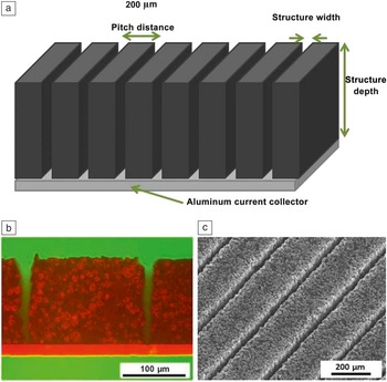
Thick films made of NMC-111 (LiNi1/3Mn1/3Co1/3O2) with thickness of 155 µm, 185 µm, and 210 µm were produced by tape casting. Reference Smyrek, Pröll, Rakebrandt, Seifert and Pfleging38 These film thicknesses are beyond the state of the art for high-power LIB (typical film thickness: 50 µm). Ultrafast laser ablation (pulse duration: 350 fs) was carried out to realize a periodic line pattern with a line-to-line distance of 200 µm ( Figure 7a ). Those electrodes were successfully tested regarding their high rate capability (i.e., for high-power application).
Laser structuring of NMC-111 thick-film electrodes. (a) Schematic view of the laser-generated pattern in thick-film NMC-111 electrodes. Scanning electron microscope image (b) (top view) and (c) (cross-section view); film thickness: 155 µm. Note: NMC, lithium nickel manganese cobalt oxide. Reference Pfleging, Mangang, Zheng, Smyrek and Pröll39

Figure 7b shows that due to ultrafast laser ablation, there is no debris formation and thermal damage such as melting of the composite electrode material. Reference Pfleging, Mangang, Zheng, Smyrek and Pröll39 Furthermore, due to the cold nature of fs-laser ablation, a high-aspect ratio of approximately 15 could be reached. Damage to the thin aluminum current collector could be avoided by careful adjustment of the laser and process parameters. A comparison of ns ablation and fs-laser ablation for structuring of NMC-111 was shown in Reference Reference Pfleging, Zheng, Mangang, Bruns and Smyrek40. For ns-laser radiation (pulse length 200 ns) the laser-beam energy is absorbed at the material surface and due to heat conduction, the temperature of the surrounding composite material increases. The poly(vinylidene difluoride) (PVDF) binder material for tape cast electrodes has a low decomposition temperature in the range of 250–350°C. Therefore, the PVDF binder matrix spontaneously evaporates and active particles are removed from the laser-beam interaction zone. Due to the thermal nature of the ns-laser ablation process, aspect ratios are significantly smaller than five and melting of active material particles might occur, especially for big NMC-particles, which are close to the laser irradiated zone. Ultrafast (fs, ps) laser ablation of electrode materials has a higher ablation efficiency than ns-laser ablation Reference Mangang, Seifert and Pfleging31 and due to the small feature size and high-aspect ratio (Figure 7b), only a small amount of active material is removed (<5%).
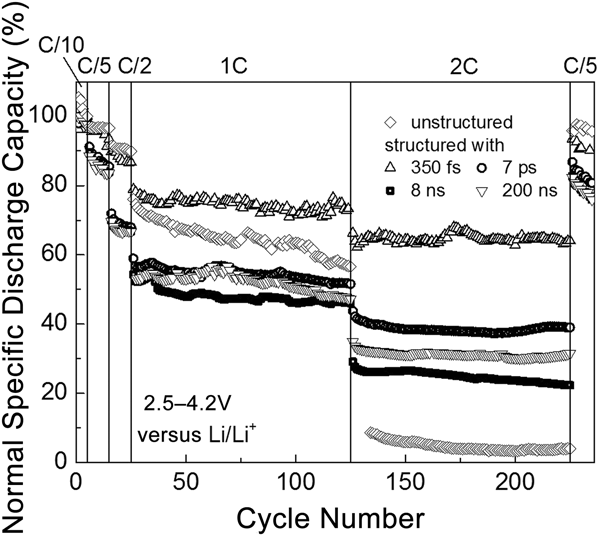
The electrochemical performance of LIB with laser structured thick-film lithium-iron phosphate electrodes was analyzed ( Figure 8 ) Reference Mangang, Seifert and Pfleging31 for different C-rates, meaning, C/2 or 2C battery discharging takes two hours or 30 minutes, respectively. Cells with unstructured thick-film electrodes reveal a strong decrease in capacity with increasing discharging current. This behavior is more pronounced with increasing film thickness. For cells with structured electrodes, this type of cell failure is avoided. Even for 2C, remarkable capacity retention for all film thicknesses could be achieved. This means high-energy and high-power LIB become possible at the same time.
Specific discharge capacity as a function of the cycle number for a cell with an unstructured lithium-iron phosphate (LFP) cathode and cells with LFP cathodes that were structured with different laser-pulse durations. Note: A “1C” or “C/5” rate means that the discharge current will discharge the entire battery in 1 or 5 h, respectively. For batteries with structured electrodes, cycle retention and specific capacity are significantly improved in comparison to batteries with unstructured electrodes. Reference Mangang, Seifert and Pfleging31 Note: fs, femtosecond; ns, nanosecond; ps, picosecond.
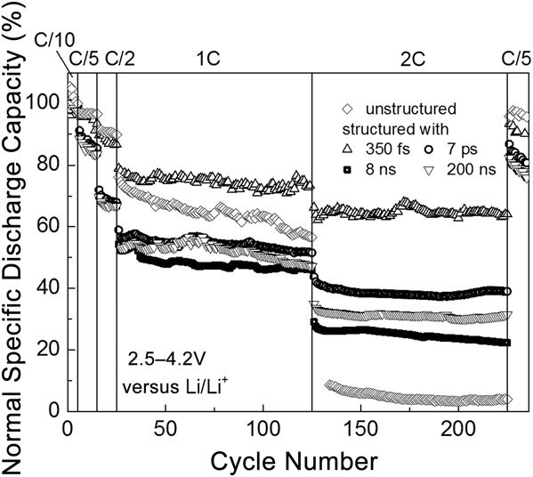
Ultrafast laser ablation of thick-film electrodes in LIB manufacturing offers great advantages for improving cell performance such as an increased battery lifetime and enhanced cycle retention for high-power and high-energy applications. The improvement of battery performance is due to an increase in lithium-ion diffusion kinetics. Reference Mangang, Seifert and Pfleging31 Furthermore, microcapillary structures down to the current collector lead to a tremendous improvement in wetting of the composite material with liquid electrolyte, which is essential for proper LIB operation. It is expected that with laser-generated microcapillary structures, higher flow rates in production lines can be achieved due to the avoidance of time-consuming cell storage accompanied by lower required storage capacities that is currently necessary to guarantee almost homogeneous electrolyte wetting. Due to spontaneous electrolyte wetting, a reduction in production failure also can be achieved. Furthermore, safety and production/yield issues improve with the use of completely wetted structured electrodes, which reduce the risk of failure and occurrence of thermal runaway as would be the case for incompletely wetted unstructured electrodes where inhomogeneous local current densities and hot spots may promote cell degradation. Current research is focused on process upscaling for large electrode footprint areas that will contribute to a significant decrease in manufacturing costs while maintaining or improving the overall battery performance and safety.
Refractive eye surgery
The unique features of ultrafast laser processing, which are the driving factors for new industrial applications, have also enabled new surgical procedures, especially in the field of refractive eye surgery. Ultrafast lasers bring precision, reliability, and safety to procedures that were previously performed manually by mechanical means.
The femto-LASIK procedure (laser-assisted in situ keratomileusis) allows changing the refractive power of the cornea to correct myopia, hypermetropia, and astigmatism. Reference Kymionis, Kankariya, Plaka and Reinstein41 The femto-LASIK process consists of three steps. First, a thin flap is cut inside the cornea by a fs laser. The flap is then lifted by the surgeon, exposing the corneal bed. A thin layer is ablated by an excimer laser, thereby modifying its curvature. After repositioning the flap, the curvature and the refractive power of the cornea have been modified. Newer procedures, such as small-incision lenticule extraction, Reference Shah, Shah and Sengupta42 which consists of the extraction of a lens from a cut inside the cornea by a fs laser, do not require the use of an additional excimer laser.
Cataract surgery can also be performed with an ultrafast laser. Reference Donaldson, Braga-Mele, Cabot, Davidson, Dhaliwal, Hamilton, Jackson, Patterson, Stonecipher and Yoo43 A cataract, a gradual opacification of the crystalline lens, can ultimately lead to blindness. In this procedure, a precise circular opening is cut in the capsule enclosing the lens (capsulorhexis). Fragmentation of the lens is then performed using a combination of laser and ultrasound. The lens debris are then extracted through laser-cut incisions, and an intraocular artificial lens is then inserted. Laser cataract surgery, in spite of limited reimbursement by insurers and public health systems, is currently undergoing rapid development.
More generally, ultrafast laser-based eye surgery offers high precision and reproducibility and is rapidly replacing more mature technology. New procedures are continuously being developed, for instance, in the treatment of glaucoma or the correction of presbyopia, and have the potential to improve the quality of life of millions of patients.
Conclusion
Commercial applications of ultrafast lasers benefit from parallel developments in three research and engineering communities, namely ultrafast laser–matter interaction, laser technology, and beam handling/delivery. Precise understanding of the laser–matter interaction processes creates new potential applications, such as surface nanostructuring in the case of “black silicon” or new high-energy/-power batteries. At the same time, laser technology advances continuously in terms of increasing the average power necessary to convert these research breakthroughs into industrial throughput and productivity. Finally, parallel processing or high-speed beam scanning allow us to take full advantage of the available powers, with examples ranging from applications in the printing industry to microelectronics packaging and eye surgery.
Acknowledgments
Karlsruhe Institute of Technology has received funding from the European Union’s Horizon 2020 Research and Innovation Program under the Marie Skłodowska-Curie Grant Agreement No. 644971. In addition, the support for laser processing of batteries by the Karlsruhe Nano Micro Facility (www.knmf.kit.edu/), a Helmholtz research infrastructure at KIT is gratefully acknowledged. R.S acknowledges support from the Swedish Research Council (VR) for his international postdoctoral grant.

Eric Mottay is President and CEO of Amplitude Systemes, France, a manufacturer of ultrafast lasers for science and industry, which he founded in 2001. He graduated from the Ecole Superieure d’Optique, Orsay, France, in 1985, and has since specialized in laser development and manufacturing. During his career, he developed and brought to the market numerous solid-state lasers. He is the author of numerous scientific papers and holds several patents in the field. Mottay can be reached by phone at +33 6 56464060 or by email at emottay@amplitude-systemes.com.

Xinbing Liu is Director of the Panasonic Boston Laboratory. He received his PhD degree from the University of Michigan in 1994. In 1998, he joined Electro Scientific Industries in Portland, Ore., as a senior R&D engineer, and worked on laser packaging technology for microelectronics industries. He then joined Panasonic Boston Laboratory as a project manager prior to becoming director in 2006. His research interests focus on developing technologies in picosecond lasers, laser manufacturing technologies, and micro-optics for Panasonic’s various products. He is a Fellow of SPIE and of the Laser Institute of America. Liu can be reached by phone at +1 617 577 1280 or by email at xinbing.liu@us.panasonic.com.

Haibin Zhang is the Director of Technology Development at Electro Scientific Industries, where he oversees new technology development, laser applications, and process development for the consumer and electronics laser equipment market. He received undergraduate degrees in physics and optical communications from Tianjin University, China, and a PhD degree in electrical and computer engineering from the University of Toronto, Canada. He has more than 15 years of experience in lasers, laser systems, and laser–material interactions. He has more than 30 patents and patent applications and is the author of more than 60 publications in the field of laser-based manufacturing. Zhang can be reached by phone at +1 503 671 5687 or by email at zhangh@esi.com.

Eric Mazur is the Balkanski Professor of Physics and Applied Physics at Harvard University, area dean of applied physics, and president of The Optical Society. An internationally recognized scientist and researcher, he leads a vigorous research program in optical physics and supervises one of the largest research groups in the Department of Physics at Harvard University. His research interests focus on spectroscopy, light scattering, the interaction of ultrashort laser pulses with materials, and nanophotonics. Mazur can be reached by email at mazur@seas.harvard.edu.

Reza Sanatinia is a postdoctoral fellow in applied physics at Harvard University. He received his PhD degree in physics (optics and photonics) from KTH Royal Institute of Technology, Sweden, in 2014. His research interests include nanophotonics, nanostructured semiconductors, and photovoltaics. His current research focuses on ultrafast laser–matter interactions at the nanoscale. He has authored or co-authored more than 25 publications in scientific journals and conferences. Sanatinia can be reached by email at sanatinia@g.harvard.edu.

Wilhelm Pfleging is Head of the Laser Materials Processing Group at Karlsruhe Institute of Technology, Germany. He has more than 20 years of experience in laser technology. His research interests include biological surfaces, microfluidics, and energy-storage systems. His current research focuses on the development of laser-assisted processes for advanced lithium-ion batteries. He has published more than 140 publications and has three patents granted and two patents pending. Pfleging can be reached by phone at +49 721 608-22889 or by email at wilhelm.pfleging@kit.edu.