I. INTRODUCTION
One-dimensional (1D) nanostructures have attracted considerable interest as potential building blocks and functional components in next generation nanoscale sensing, nanoelectromechanical systems (NEMS), circuits, and interconnect applications.Reference Lieber and Wang1 One-dimensional nanostructures can be quickly and reliably produced using bottom-up synthesis techniques. The reliable, reproducible, and robust integration of nanowires into systems and devices, however, remains a challenge. Postsynthesis steps have been developed for the purpose of manipulating and transferring 1D nanostructures into place.Reference Lieber and Wang1 These postsynthesis techniques tend to be complex often requiring numerous processing steps. These steps can be avoided by developing direct integration techniques where the nanostructures grow into place and form desired contacts in situ. The localized nanostructure synthesis approach, for example, could contribute to simplified 1D nanostructure-based device integration while providing a highly process-compatible solution. In this approach, bottom-up synthesis reactions are carried out on chip using a spatially confined heat source, which restricts the high-temperature exposure of the chip while permitting localized nanostructure growth and thus enabling site-specific nanostructure integration among various device components.Reference Englander, Christensen and Lin2, Reference Sosnowchik, Lin and Englander3 In this work, we consider localized heating realized upon the resistive heating of microscale line heaters. The range of material systems successfully realized using the localized heating approach has been largely limited to carbon nanotubesReference Englander, Christensen and Lin2, Reference Sunden, Wright, Lee, King and Graham4–Reference Englander, Christensen and Lin13 although the use of silicon nanowires has been demonstrated as well.Reference Englander, Christensen and Lin2, Reference Englander, Christensen and Lin13–Reference Kallesøe, Wen, Mølhave, Bøggild and Ross17 Here, we demonstrate for the first time the localized synthesis of germanium nanowires (GeNWs) on suspended microelectromechanical systems (MEMS) microbridges which serve as the microscale heaters. Due to its material properties and favorable synthesis conditions, interest in germanium as a building block and functional material for next generation nanoscale applications has flourished in recent years.Reference Jin, Yang and Jo18–Reference Adhikari, Marshall, Goldthorpe, Chidsey and McIntyre22 More specifically, synthesis temperatures for GeNWs are over 100 degrees lower than that of silicon nanowires and thus offer a distinct advantage. Additionally, germanium boasts higher electron and hole mobilities which may lead to faster electronic devices. The lower synthesis temperature is also well suited for the localized heating approach as the power input to the microbridge is reduced eliminating current runaway which is often noted with silicon microbridges at elevated temperatures.Reference Chui, Asheghi, Ju, Goodson, Kenny and Mamin23 While nanowires synthesized using standard bottom-up techniques have been well-characterized experimentallyReference Adhikari, Marshall, Chidsey and McIntyre19–Reference Adhikari, Marshall, Goldthorpe, Chidsey and McIntyre22, Reference Cui, Lauhon, Gudiksen, Wang and Lieber24–Reference Cho and Kamins30 and theoretically,Reference Tan, Li and Gosele31–Reference Wacaser, Dick, Johansson, Borgstrom, Deppert and Samuelson35 nanowires synthesized under temperature variations such as those realized in locally heated reactions have received very limited attention. The experimental setup for localized synthesis using MEMS microbridge-based heating introduces two independent temperature gradients during the synthesis process; a temperature distribution along the microbridge’s surface and a temperature gradient along the length of the growing nanowire between its base and its tip. While the former is an inherent property of resistive heaters of uniform cross section, the latter is enabled by our specific synthesis conditions. In this work, we also compare the localized synthesis results with established synthesis processes conducted in a uniform temperature environment and in so doing begin to consider the role and impact of the localized heat source and local temperature gradients on the resulting nanowires as well as the attributes of the localized synthesis process. This study therefore provides new insights to the vapor-liquid-solid (VLS) bottom-up synthesis process for GeNW synthesis. Additionally, this work contributes to the understanding of direct micro-nano integration processes and thus to advancing nanomanufacturing techniques.
II. EXPERIMENTAL METHODS
Our experimental setup is designed to accommodate both uniform temperature synthesis reactions and localized heating based synthesis reactions. We leverage VLS synthesis reactions in all experiments. All experiments are conducted within a low-pressure chemical vapor deposition (LPCVD) unit equipped with a 3-in.-diameter tubular synthesis chamber. In all of the experiments, the samples were placed in the same location within the synthesis chamber where fully developed flow conditions exist. We first established synthesis conditions for GeNWs in a uniform elevated temperature environment and use these conditions for all experiments. Based on satisfactory synthesis results, 40 sccm of germane (10% GeH4 in H2) and 100 sccm of hydrogen at a total constant chamber pressure of 80 Torr were selected as the synthesis parameters for this study and thus serve as the basis for comparison among the uniform temperature and the locally heated reactions. A sputtered gold thin film (2–3 nm thick) serves as the catalyst in all experiments and so the breakdown of the thin film into gold nanoparticle nucleation sites is determined by the conditions of the synthesis process. In all experiments, the chamber is purged with H2 prior to and following the synthesis step. The synthesis process time is varied from 1 to 30 min at which point the GeH4 supply is terminated and subsequently the chamber is allowed to cool in a H2 ambient. The time-dependent experiments are conducted to ensure that any synthesis time effects are captured. Due to the strong temperature dependence of the GeNW synthesis process,Reference Kodambaka, Tersoff, Reuter and Ross21, Reference Kamins, Li, Williams and Liu25, Reference Cho and Kamins30 the uniform temperature process is studied at constant temperature within the 230–350 °C temperature range. The temperature-dependent experiments are an important component in the analysis of the locally heated synthesis results. A single-crystal silicon substrate is used in all uniform temperature experiments.
Apart from the implementation of heating, identical synthesis conditions (40 sccm of 10% GeH4 in H2, 100 sccm of H2, and a total chamber pressure of 80 Torr) are maintained in the uniform elevated temperature and localized heating processes. For the localized process, suspended highly doped silicon and polysilicon microbridges are utilized as resistive heaters, which generate the thermal environment required for synthesis. A variety of microbridge geometries (2–15 μm thick, 4–5 μm wide, and 150–200 μm long) and designs have served as functional synthesis platforms. Additional information about microbridge design, fabrication, and characteristics is available elsewhere.Reference Englander, Christensen and Lin2, Reference Sosnowchik, Lin and Englander3, Reference Englander, Christensen and Lin13, Reference Englander, Christensen, Kim, Lin and Morris14 Using a vacuum feedthrough, power is supplied to individual microbridges inside the chamber to realize a localized temperature increase via resistive heating. The level of heating is regulated by the power input to the microbridge, which is evaluated based on the real-time current-voltage relation for the microbridge.Reference Englander, Christensen and Lin2 Power input required for the synthesis of GeNWs is reduced when compared to the power input required to achieve sufficient heating for the synthesis of silicon nanowires or carbon nanotubes.Reference Englander, Christensen and Lin2 This is consistent with the comparatively lower synthesis temperature required for the bottom-up synthesis of GeNWs. When compared with Englander et al. previous worksReference Englander, Christensen and Lin2, Reference Englander, Christensen and Lin13–Reference Englander, Christensen, Kim and Lin15 and our ongoing localized silicon nanowire synthesis work, we note a significant improvement in yield with locally synthesized GeNWs, which we attribute to the reduced temperature requirement and thus the elimination of current runaway and localized melting of the silicon microbridge. To maintain consistency with the uniform, elevated temperature processes, the microbridge temperature is increased prior to the onset of GeH4 flow. Sufficient microbridge heating is achieved within 5 min, and the microbridge experiences the H2 environment prior to GeH4 flow. The localized heating and thus the synthesis process is maintained for 15–20 min at which point the GeH4 supply is terminated and subsequently the power to microbridge is slowly reduced.
Our evaluation is focused on a comparative quantitative study of resulting nanowire geometry, nanowire growth rates, and nanowire quality. Nanowire geometry is assessed in terms of nanowire diameter, length, and taper. We define a taper as the change in nanowire diameter through the length of the nanowire and report a quantity which is measured in nanometers per micrometers. Nanowire quality is assessed in terms of nanowire kinking or the formation of sharp bends along the nanowire. We also address branching behavior in locally synthesized nanowires; a phenomenon that is never observed in our uniform temperature processes. The analysis presented here is based on measurements of over 400 individual nanowires. ImageJ software is used to perform the measurements.
III. RESULTS AND DISCUSSION
A. Synthesis results
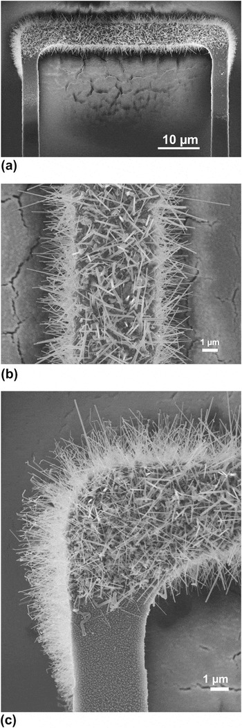
We first present the results of the localized synthesis of GeNWs as this is a first demonstration with this material system. The localized synthesis of GeNWs on a single-crystal silicon microbridge is seen in Fig. 1. GeNW growth covers approximately 50% of the microbridge’s surface. The presence of GeNWs is confirmed using elemental analysis. The resistive heating yields a parabolic temperature distribution along the length of the microbridge where the center of the structure experiences the highest temperature and anchor locations remain at room temperature. Interestingly, this experimental setup essentially enables multiple temperature-dependent synthesis reactions to be conducted within a single experiment. The extent of the growth region is determined by the local surface temperature where at sufficiently reduced temperatures the synthesis reaction can no longer take place. Since the GeNW growth in Fig. 1 is continuous throughout the high-temperature region, it can be concluded that at no point along the length of this microbridge is the surface temperature too high to support the reaction. Additional thermal effects and particularly the implications to the VLS mechanism are discussed in the following sections.
Localized germanium nanowire (GeNW) synthesis results. (a) Nanowire growth along approximately 50% of a single-crystal silicon microbridge. (b) A closeup view of the central region of the microbridge where the surface temperature is the highest; nonuniformity in both nanowire diameter and length is noted. (c) Nanowire growth at a corner location, a cooler location of the microbridge; the nanowire growth–no growth boundary along with nanowire kinking is observed. Nanowires synthesized at cooler locations of the microbridge are typically of smaller diameter than those synthesized at central, warmer locations of the microbridge.

As seen in Fig. 1 we note significant variations in nanowire diameter and length within a given growth region along the microbridge. For example, nanowire tip diameters range from 20–200 nm and lengths range from less than 1 to over 7 μm within a 2-μm-long region of the microbridge where fairly small changes in temperature are expected. No long-range or short-range nanowire organization is observed within the growth region. The larger diameter nanowires are typically the longer nanowires consistent with the reported increase in growth rates as a function of increasing nanowire diameter.Reference Dayeh and Picraux28, Reference Schmidt, Senz and Gosele34 In this work, we refer to the nanowire’s tip diameter rather than the base diameter due to changes in diameter along the length of the nanowire, which is a fairly prevalent result in GeNW synthesis. For this analysis, we also group nanowires by their diameter; small diameter nanowires are <100 nm in tip diameter and large diameter nanowires are >100 nm in tip diameter. The average diameter for the locally synthesized small diameter nanowires is 57 nm (standard deviation 20 nm), and the average diameter for the locally synthesized large diameter nanowires is 148 nm (standard deviation 33 nm). Regions of the larger diameter nanowires are typically but not exclusively situated at central regions of the microbridge where the temperature is higher [Fig. 1(b)]. The small diameter nanowires are abundant throughout but are prevalent at cooler regions of the microbridge as seen in Figs. 1(b) and 1(c). We compute a growth rate by dividing the total nanowire length by the total time that the germane precursor is present in the chamber. Overall, the locally synthesized nanowires exhibit a growth rate of 0.2 μm/min. More specifically, the small diameter nanowires exhibit at growth rate of 0.18 μm/min (standard deviation 0.09 μm/min), while the large diameter nanowires grow at a slightly higher growth rate of 0.25 μm/min (standard deviation 0.03 μm/min). Additionally, an individual nanowire’s growth rate depends on its location along the microbridge, which directly correlates to the surface or synthesis temperature. Along the surface of the microbridge, the highest growth rates are typically measured at central regions. Differences in growth rates, among the fastest and slowest growth regions, have been observed to range from 0.06 to 0.15 μm/min.
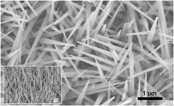
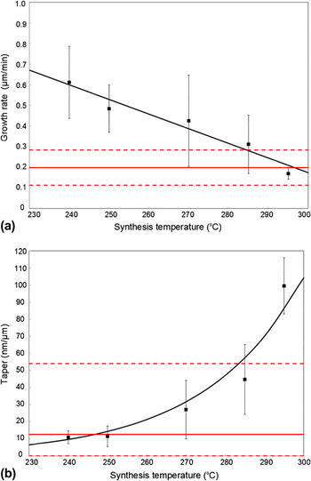
Figure 2 illustrates GeNWs synthesized following a 15-min-long synthesis process conducted at a uniform and constant chamber temperature of 285 °C and otherwise identical synthesis conditions to the localized experiments described above. Within a similar growth region to the one analyzed in the localized sample, great uniformity in nanowire diameter and length is noted. The average tip diameter is 63 nm (standard deviation 21 nm), and we note that the uniform temperature reactions yielded exclusively small diameter nanowires. We presume that the greater uniformity in nanowire diameter is in part due to the uniform conditions during which the thin gold film turns into nucleation sites for the synthesis reaction. The growth rate is strongly tied to the synthesis temperature and for the uniform temperature processes ranges from an average peak rate of 0.6 μm/min at 240 °C and is reduced to 0.17 μm/min at 295 °C. The decrease in growth rate at elevated temperatures is somewhat counterintuitive, however, the availability of the vapor phase reactant must be considered. We speculate that at and above germane’s thermal-decomposition temperature (∼280 °C),Reference Tamaru, Boudart and Taylor36, Reference Hall37 both axial (nanowire) and lateral (noncatalyzed) growth reactions are competing for the availability of germane; while at reduced temperatures, the incoming germane is completely available for nanowire synthesis hence contributing to higher growth rates. For uniform temperature reactions, we observe a weak correlation between growth rate and diameter. While similar observations have been made by others,Reference Ross29 our narrow diameter distribution could affect this finding as well. The data do suggest a linear relationship between growth rate and temperature as presented in Fig. 3(a). We superimpose the average growth rate for the locally synthesized nanowires onto this plot. Although, initial observations may suggest that the locally heated synthesis reactions should successfully take place above ∼280 °C, we present more complex relationships in the following sections.
Uniform temperature GeNW synthesis results. GeNW synthesis at 285 °C yields nanowires of highly uniform diameter, length, and taper. Significant tapering is evident in these nanowires; a behavior which is not prevalent with nanowires synthesized using a localized heating source. Inset illustrates uniformity across the sample.

Comparing uniform temperature and localized heating processes for GeNWs. Synthesis temperature is seen to affect both growth rate and the tendency for tapering. (a) A linear relationship between GeNW growth rate and synthesis temperature (black line) for uniform temperature processes. As the synthesis temperature increases, the axial nanowire growth rate is reduced. Growth rates for locally heated reactions are superimposed on the plot; the solid red line represents the average growth rate (considering all locations along the microbridge) and the dashed red lines represent the standard deviation of the data. (b) An exponential relationship between nanowire taper and synthesis temperature (black line) for uniform temperature processes. As the synthesis temperature increases, the nanowires exhibit increased taper values. Taper values for locally heated reactions are superimposed on the plot; the solid red line represents the average taper value (considering all locations along the microbridge) and the dashed red lines represent the minimum and maximum taper values measured.

B. Nanowire tapering
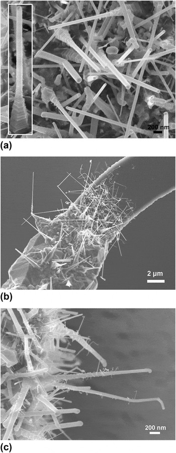
The thermal decomposition or noncatalyzed decomposition of germane is known to proceed at measurable rates above 280 °C.Reference Tamaru, Boudart and Taylor36, Reference Hall37 The noncatalyzed decomposition of germane is known to contribute to a characteristic taper that is commonly observed with GeNWs and as seen in Fig. 2.Reference Dayeh and Picraux28 In Fig. 3(b), we present the average taper value as a function of synthesis temperature for nanowires synthesized at uniform temperatures. We note a strong exponential correlation where large taper values are observed at the highest synthesis temperatures. An average taper value of 10.9 nm/μm is recorded for nanowires synthesized at 240 °C and this value increases nearly 10 times for nanowires synthesized at 295 °C. We superimpose the average taper value for nanowires synthesized in the locally heated environment onto the plot in Fig. 3(b). The average taper value for locally synthesized nanowires is 12.6 nm/μm, where ∼20% of locally synthesized nanowires exhibit no taper. In contrast to the growth rate comparison [Fig. 3(a)], the taper analysis suggests that localized synthesis reactions yield results consistent with synthesis temperatures below ∼280 °C. The locally heated synthesis processes further provide interesting insights to the tapering mechanism. Figure 4(a) illustrates partial tapering along locally synthesized nanowires where we suspect that the temperature requirements for noncatalyzed germane decomposition are met at the microbridge’s surface (T > 280 °C), but as the temperature along the length of the nanowire is reduced as it grows away from the surface, tapering ceases and a uniform diameter nanowire results. We hypothesize that the thermal gradient and more specifically the temperature drop through the length of the nanowire makes the local environment less suitable for the noncatalyzed thermal decomposition of germane thus halting this growth mode. Thus, the taper rate or the change in diameter is not necessarily constant along the length of the locally synthesized nanowires. Instead it appears that noncatalyzed germanium deposition takes place within certain proximity of the base (∼0.8 μm) where the temperature is sufficient. Tapered nanowires are typically observed in central regions of the microbridge suggesting a temperature threshold for noncatalyzed germanium deposition. Nontapered nanowires are typically located at cooler regions of the microbridge. Additionally, tapering in locally synthesized nanowires is visually different than the characteristic taper in the uniform synthesis environment. While the side walls of the uniform temperature synthesized nanowires are rather smooth and the taper rate is constant (Fig. 2), tapered portions of the locally synthesized nanowires are rougher and appear heavily faceted [Fig. 4(a)]. Reduced tapering leads to a uniform cross section along the length of the nanowire which could increase electron mobility efficiencyReference Xiang, Lu, Hu, Wu, Yan and Lieber38 and decrease the stiffness of the nanowire; both are favorable for integration and device applications.
Unique observations in locally synthesized GeNWs. (a) Noncatalyzed germanium deposition produces nanowires with a wide base which turn into uniform diameter nanowires as nanowires extend away from the microbridge’s surface; inset illustrates a 1.9-μm-long nanowire with a 450-nm-wide base and a tip diameter of 97 nm where the highly tapered region extends for 0.86 μm from the microbridge’s surface. (b) An illustration of the temperature window that supports localized GeNW synthesis along the surface of a curved microbridge: the nanowire growth region is bounded by germanium film-like deposition in high-temperature regions and no nanowire growth at low-temperature regions. Instances of branch formation, near the base of the nanowires, are observed as well. (c) A closeup view of nanowire branches growing along the surface of a main nanowire which originates at the microbridge’s surface. The branches do not extend to the tip of the main nanowire suggesting that nucleation sites and/or conditions for nanowire synthesis may only available within a particular proximity to the base.

C. Nanowire kinking
Kinking or sharp bends along the length of the nanowire have been attributed to a disturbance of the local equilibrium in the bottom-up synthesis reactions. More specifically, changes to the liquid alloy and/or changes at the liquid–solid interface brought upon by variations in either pressure or temperature are known to affect the synthesis results.Reference Madras, Dailey and Drucker27, Reference Wagner and Doherty39, Reference Tian, Xie, Kempa, Bell and Lieber40 The presence of kinks may have implications to defect formation within the nanowire,Reference Molhave, Wacaser, Petersen, Wagner, Samuelson and Boggild16, Reference Madras, Dailey and Drucker27, Reference Wagner and Doherty39, Reference Lee, Woo, Yang, Lee, Kim and Jo41 and thus it is important to study the conditions that contribute to their formation. As seen in Fig. 2, when synthesized in a uniform temperature environment, our nanowires do not exhibit any kinking or bending. However, the locally synthesized nanowires do exhibit significant kinking and bending. Since synthesis reactions take place at constant chamber pressure, we suspect that axial temperature gradients, formed between the microbridge surface and the tip of the nanowire, perpetuate this behavior. We determine a linear kinking density, which is defined as the number of sharp kinks along the length of the nanowire per micron of nanowire length. Additionally, we use the term length-to-first-kink as a measure of the distance away from the microbridge surface where a nanowire first kinks and its growth direction changes. As kink formation may also be due to end-of-process conditions, no nanowires which exhibit significant kinking in the vicinity of the nanowire tip (within 500 nm) contribute to this analysis. As a function of diameter, we note an increase in kinking density in the smaller diameter nanowires. This observation is illustrated in Fig. 1 as well as Figs. 4(a) and 4(b). The kinking density for locally synthesized small diameter nanowires ranges from no kinks to a maximum of 2.6 kinks/μm and an average of 1.0 kinks/μm (average value considers only kinked nanowires). The kinking density for locally synthesized large diameter nanowires ranges from no kinks to 1.1 kinks/μm with an overall average of 0.62 kinks/μm (average value considers only kinked nanowires). It is important to note that we observe no kinking in 54% of the locally synthesized large diameter nanowires while only 35% of the small diameter nanowires exhibit no kinking. We also note a correlation between nanowire diameter and the length to first kink. On average, the first kink for large diameter nanowires occurs at ∼2.4 μm away from the surface of the microbridge while the first kink in the small diameter nanowires occurs at ∼1.6 μm away from the surface of the microbridge. Molhave et al.,Reference Molhave, Wacaser, Petersen, Wagner, Samuelson and Boggild16 using a similar microbridge setup, noted kinking only on nanowires growing away from the microbridge, on outer surfaces, while for nanowires growing along the inner surfaces of the microbridge, where a more uniform temperature is maintained, no kinking was observed. We have not observed location-dependent kinking, but perhaps the shorter distance between the legs of the microbridge in Molhave et al. work’s contributes to improved temperature uniformity than with our microbridge design. Since the kinking and bending often appears near the free end of the nanowire, we may also infer that the end-of-process synthesis conditions could affect this result. Lee et al.Reference Lee, Woo, Yang, Lee, Kim and Jo41 have noted kinking at silicon nanowire tips under an imposed temperature gradient, but the thermal gradient was reversed from the setup in this work. Although in both the local and uniform temperature experiments the vapor phase reactant is terminated prior to cool down, the rate of cooling may play an important role. The furnace environment is heated and cooled at a rate of a few degrees per minute, while the microbridge can realize similar temperature changes within a few seconds. Ongoing experiments are designed to assess whether the time frame between the termination of germane flow, the presence of residual germane in the chamber, and the cool down of the microbridge affects nanowire bending and kinking near the tip.
D. Dynamics of locally heated synthesis reactions and nanowire branching
Bottom-up reactions for nanowire synthesis are known to be effected by a wide range of parameters. The temperature gradients associated with the localized heating regime introduce new aspects to the evaluation of the synthesis results. In this section, we utilize our observations along with findings from the literature to better characterize the localized synthesis process. The growth rate, for example, is typically affected by the synthesis temperature, pressure, nanowire diameter, and the overall dynamics of the VLS process.Reference Kodambaka, Tersoff, Reuter and Ross21, Reference Dayeh and Picraux28, Reference Ross29, Reference Chen and Cao32, Reference Dubrovskii and Sibirev42, Reference Chen and Cao43 As expected, we have noted growth rate variations as a function of location along the microbridge. Interestingly and in contrast to our uniform temperature processes, we do not observe an increase in growth rate at cooler regions of the microbridge. Variations in nanowire diameter and the axial temperature gradient along each nanowire are likely contributing to this observation and hinder a direct correlation among the samples. While conflicting reports are presented in the literature with respect to the correlation of a nanowire’s diameter with its growth rate,Reference Dayeh and Picraux28, Reference Ross29 we have noted a slight increase in growth rate with increasing diameter for locally synthesized nanowires. The role of gradually reduced temperatures at the tip with increasing nanowire length must also be considered when growth rates are examined. Both the kinking and tapering behavior described previously suggest a temperature change along the nanowire and the former provides an indication of changes at the nanocluster catalyst. This would suggest that growth rates in the locally heated reactions are impacted by the decreasing catalyst temperature as the catalyst moves away from the heated microbridge. Thus, a nonuniform growth rate, and more specifically, a decreasing growth rate with increasing nanowire length, is likely in place. We hypothesize that as a function of nanowire diameter, nanowire array density and synthesis conditions, there may be an upper limit on the length a nanowire may reach as the temperature at the tip may decrease sufficiently to terminate the reaction. Similar, although preliminary, observations have been reported for silicon nanowire synthesis.Reference Reguer and Dallaporta44 We are currently assessing this effect quantitatively.
Based on recent worksReference Kodambaka, Tersoff, Reuter and Ross21, Reference Adhikari, Marshall, Goldthorpe, Chidsey and McIntyre22, Reference Gamalski, Tersoff, Sharma, Ducati and Hofmann45 and our experimental synthesis temperature, our uniform temperature synthesis processes may be described by a subeutectic VLS mechanism. The germanium-gold eutectic temperature for bulk materials is 361 °C and thus our synthesis processes occur at bulk subeutectic temperatures. The current literature, however, points to melting point and potentially eutectic point depression for nanostructures, strong size-dependent phase behavior as well as evidence of a germanium–gold liquid catalyst at temperatures as low as 240 °C.Reference Kodambaka, Tersoff, Reuter and Ross21, Reference Ross29, Reference Gamalski, Tersoff, Sharma, Ducati and Hofmann45–Reference Sutter and Sutter47 These findings suggest that VLS synthesis could take place well below the specified eutectic temperature. VLS synthesis of GeNWs has been reported at up to 400 °C,Reference Kodambaka, Tersoff, Reuter and Ross21, Reference Cho and Kamins30 but our uniform temperature processes, at the conditions described above, have been successful only up to 300 °C. At elevated temperatures, we observe island formation and eventually the formation of a germanium thin film. Our uniform temperature processes are successful down to 240 °C; while at 230 °C, no GeNW synthesis is observed. The locally heated reactions do visually define thermal boundaries for nanowire growth. As seen in Fig. 4(b), we have observed germanium film-like deposition, rather than nanowires, locally along the microbridge at regions heated beyond the nanowire synthesis temperature and a fairly abrupt transition to nanowire growth at cooler regions of the microbridge and no growth at yet cooler regions. Thus an ideal temperature window for the synthesis reaction must exist. The comparisons to the uniform temperature synthesis reveal characteristics consistent with the 240–300 °C temperature range.
Instabilities in the nanowire synthesis reaction under localized heating conditions may be further inferred from evidence of branching, which like kinking is never observed in our uniform temperature processes. In fact, branching has yet to be reported with locally heated synthesis reactions in other material systems. Branching is defined by small diameter nanowires, which protrude laterally from a nanowire growing from the microbridge’s surface. The occurrence of branching requires nucleation sites along the length of the growing nanowire. Examples of branching are shown in Figs. 4(b) and 4(c). Branching behavior for VLS-synthesized microwires was first described by Wagner and DohertyReference Wagner and Doherty39 and this phenomena is closely tied with the formation of kinks. Similar to our observed nanowire kinking, nanowire branching appears to occur at various locations along the microbridge and yet is only observed for some of the nanowires. Wagner and Doherty attributed branching to nonisothermal VLS processes where a temperature drop induced a decrease in the volume of the liquid alloy, which was required to satisfy phase equilibrium. The process of the reduction in volume was then associated with the disintegration of the liquid alloy, which resulted in small droplets of the catalyst deposited along the length of the nanowire enabling the growth of nanowires, or branches, along the main nanowire. Others have observed the migration of gold from the liquid alloy as a function of synthesis temperature, as well as precursor availability and partial pressure.Reference Kawashima, Mizutani, Nakagawa, Torii, Saitoh, Komori and Fujii48–Reference Dhalluin, Desre, den Hertog, Rouviere, Ferret, Gentile and Baron50 Branching in our locally synthesized GeNWs is rarely observed for nanowires with diameters smaller than 40 nm. Nanowire branches are typically 15–20 nm in diameter and always smaller than the main nanowire. It is interesting to note that branching is typically confined to 60–70% of the total nanowire length or up to 2 μm away from the surface of the microbridge. For silicon nanowire synthesis, Gentile et al.Reference Gentile, David, Dhalluin, Buttard, Pauc, Hertog, Ferret and Baron49 reported that it is possible to significantly reduce gold diffusion from the catalyst by decreasing the synthesis temperature in situ. We suspect that with the reduction in tip temperature as a function of increasing nanowire length (∼10–20 degrees/μm within 2 μm from the microbridge’s surface), particularly at cooler regions of the microbridge, the tendency for gold diffusion is reduced thus reducing nucleation sites for branched growth in the proximity of the tip. However, we also observe a reduction in the main nanowire’s diameter which is consistent with some yet minor loss of the catalyst. Thus, it is also likely that gold nanoparticles are present throughout the length of the nanowires as is evident in Fig. 4(a). Therefore variations in supersaturation requirements as a function of catalyst size and temperature may explain the presence and absence of branching.Reference Sutter and Sutter47, Reference Dhalluin, Desre, den Hertog, Rouviere, Ferret, Gentile and Baron50, Reference Schwalbach and Voorhees51 The required supersaturation or germanium content has been shown to increase with decreasing catalyst diameter,Reference Schwalbach and Voorhees51 and a reduction in the size of migrated gold with increasing nanowire length is expected. Further, gold catalysts near the base of the nanowire are subjected to the synthesis conditions for longer time periods, enabling catalyst migration, coalescence, and sufficient opportunity for nanowire growth. We note, however, that in similar localized synthesis experiments with silicon nanowires, branching behavior is prevalent through the full length of the nanowire.Reference Redcay52 This observation may be explained by the higher temperatures required for silicon nanowire synthesis and the reported weaker dependence of the supersaturation requirement as a function of diameter for silicon nanowires.Reference Schwalbach and Voorhees51 Additionally, the absence of branching at regions of higher temperature, for example, at central regions of the microbridge [Fig. 4(a)], may be explained by the increase in supersaturation required for nucleation.Reference Adhikari, Marshall, Goldthorpe, Chidsey and McIntyre22, Reference Sutter and Sutter46, Reference Schwalbach and Voorhees51 In the future, the ability to control branching behavior can be useful in the self-assembly of three-dimensional nanowire-based networks.
IV. CONCLUSIONS
To conclude, we report on the synthesis of GeNWs using a localized heating technique to yield spatially confined synthesis regions and thus a viable method for direct nanowire integration. The localized synthesis reaction is compared to GeNW synthesis performed in uniform thermal environments under otherwise identical synthesis conditions. This work illustrates that the thermal environment affects the synthesis process dynamics and therefore the resulting nanowires. The implementation of locally heated bottom-up synthesis reactions introduces unique aspects to the synthesis process, which in turn contribute to unique findings but also trends of increased complexity. We note a reduction in growth rate and elevated kinking levels in locally synthesized nanowires when compared to nanowires synthesized in uniform temperature processes. We believe that the nanowires’ growth rate is not constant and instead decreases with increasing nanowire length. Additionally, we note a reduction in the nanowires’ tendency to taper along with a distinctive expression of the taper. Finally, we observe a unique branching behavior. This work offers new insights to the VLS mechanism, however, the effects of this heat source implementation on material and structural properties of the nanowires has yet to be assessed in depth. This work clearly illustrates that in order for localized VLS synthesis reactions to play a significant role in the fabrication and assembly of next generation nanowire-based systems and devices, we must fully understand synthesis process–nanostructure property relationships.
ACKNOWLEDGMENT
This work was completed with the support of the Florida State University’s start up funds.