Introduction
Subwavelength microlens is one of the emerging planar micro-optical devices with great potential in a variety of applications.[Reference Jahani and Jacob1–Reference Ye and Yi8] Among this field, high refractive index contrast nanostructures show great advantages in areas such as spectral modification of optical wave front.[Reference Chang-Hasnain2] These advantages have enabled the microlens to be designed in a scale ranging from micrometers to several millimeters with focus size less than a micrometer.
Based on the subwavelength nature of phase shifters, the physical realization of the microlens relies on nanofabrication techniques. To be specific, it can be either fabricated through reactive ion etching (top-down process) or deposition then lift-off (bottom-up process). Despite the difference in the process details, both of the two techniques have one common challenge that it is extremely difficult to fabricate structures with a high aspect ratio (e.g., a ratio higher than 5:1 thickness versus width). For planar grating lens that is designed under linearly polarized incidence (e.g., utilization of propagation phase,[Reference Chang-Hasnain2, Reference West, Stewart, Kildishev, Shalaev, Shkunov, Strohkendl, Zakharenkov, Dodds and Byren4] not Pancharatnam–Berry phase), the different phase shift is created by altering the effective refractive index. To achieve enough phase shift in visible wavelength with limited thickness (e.g., low aspect ratio), researchers have looked into high refractive index materials such as GaN[Reference He, Wang, Liu and Wang3] and TiO2.[Reference Wang, Miao, Tian, Guo, Zhang, Ren and Liu9] While high refractive index materials are enabling phase shifters more phase shift with comparatively low aspect ratio, their transmission may experience a significant drop.
To design an optimum planar microlens, one should either increase the phase coverage of low-index material nanostructures or increase the transmission of high-index material nanostructures. While the most effective way of increasing phase coverage of nanostructures is to increase its thickness (increase single-mode propagation length inside the structure). This idea may not be practical, as we already approaching the limit of current nanofabrication with 80 nm of feature size and 400 nm of thickness. Upon realizing this, we have to consider another direction as mentioned previously, which is to increase the transmission of high-index material nanostructures.
In this work, we have discussed possible transmission enhancement mechanisms and their feasibilities with the application of planar microlens. In addition, we have proposed the subwavelength-tapered nanostructure to enhance the transmission of TiO2 nanostructure as phase shifters of microlens under the linearly polarized light. The enhancement effect is then examined by numerical simulation [finite different time domain method (FDTD)] through the subwavelength micrograting lens in a two-dimensional (2D) domain.
Design and simulation results
The design of subwavelength micrograting lens follows a widely acknowledged phase-matching process.[Reference He, Wang, Liu and Wang3–Reference Fattal, Li, Peng, Fiorentino and Beausoleil6] Basically, the micrograting lens consists of a group of phase shifters (e.g., subwavelength nanogratings defined by a period and fill factor[Reference Chang-Hasnain2, Reference Duan, Zhou, Huang, Shang and Ren5]) that each of them will tune the phase of light (that pass through this phase shifter) based on its dimension and refractive index. To be specific, the phase profile of a typical focusing subwavelength-grating lens is governed by the equation:
 $$\phi \,(x) - \phi \,(0) = \displaystyle{{2\pi} \over \lambda} \left( {\sqrt {x^2 + f^2} - f} \right) = - \Delta \phi, $$
where λ is the incident wavelength, f is the designed focal length, x is the distance between the phase shifter and the center of the lens, ϕ (x) is the phase needed for this phase shifter, and ϕ (0) is the phase at the center of the lens. Δϕ is the phase difference created by the nanostructure at this location. For micrograting lens, necessary phase shifts [e.g., ϕ (x)] can be acquired through different subwavelength nanostructures (gratings) defined by a period and fill factor (also known as duty cycle[Reference West, Stewart, Kildishev, Shalaev, Shkunov, Strohkendl, Zakharenkov, Dodds and Byren4, Reference Duan, Zhou, Huang, Shang and Ren5]). In other words, the focusing subwavelength-grating lens is designed by selecting appropriate grating structures to fulfill the phase profile of a focusing lens [e.g., Eq. (1)].
To compare the phase shift and transmission of high-index and low-index nanostructures, we have chosen two materials, Si3N4 (refractive index 2.0) and TiO2 (refractive index 2.55), and conducted the study through 2D FDTD under the light incidence of 685 nm, as shown in Fig. 1. Nanostructures in Fig. 1 are defined by a period and fill factor (also known as duty cycle), and the dimensions presented here cover the most conventional phase shifter dimensions in a 2D domain. Perfect match layer is applied on the boundaries (both ends) of the incident direction to truncate the simulation area. Periodical boundary condition is applied (on other two boundaries) for the extension of grating during the creation of phase map. Sufficiently long time steps and sufficiently small grid size are utilized to ensure the precision of FDTD simulation. The refractive index of air is set as 1 and the phase shifter is mounted on a glass substrate with a refractive index of 1.5. The imaginary part of the refractive index is neglected.
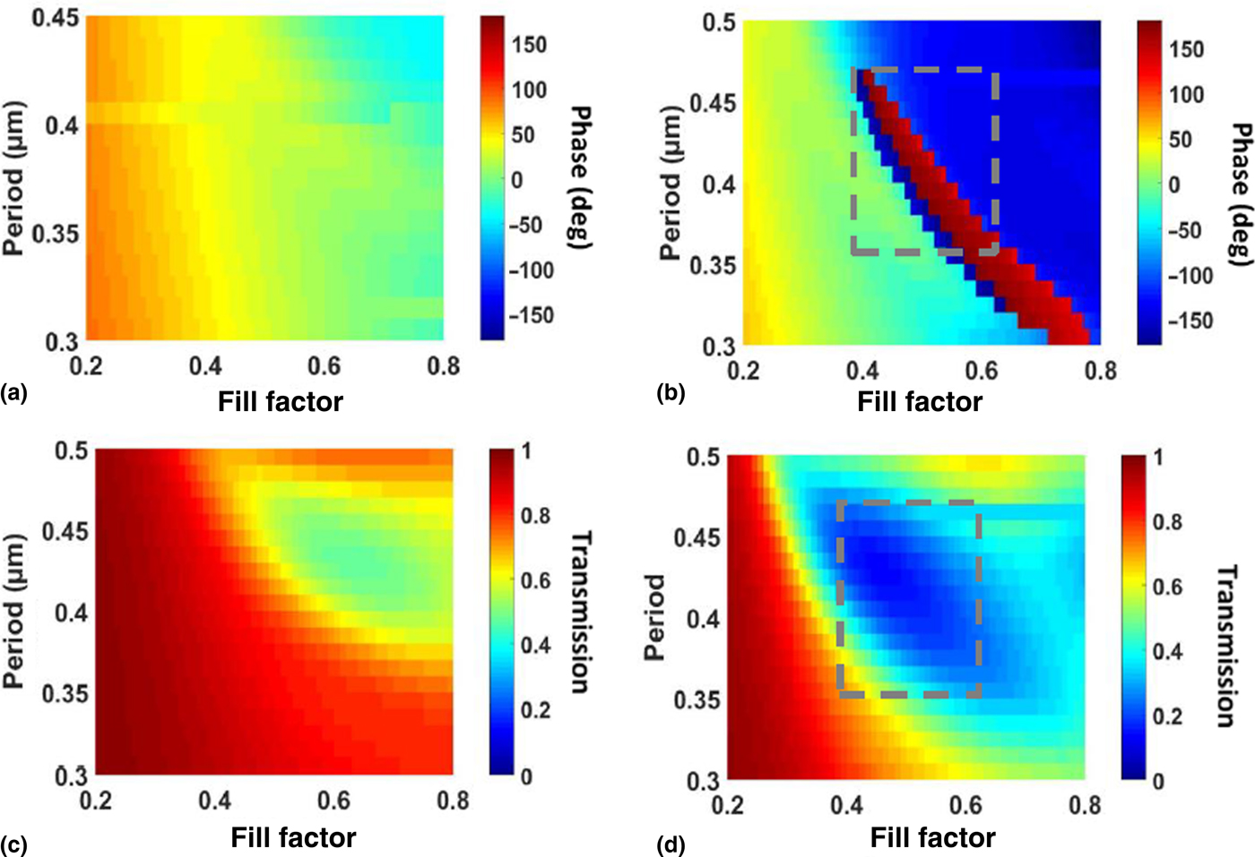
Phase diagrams and transmission for single phase shifters with a thickness of 400 nm. (a) Phase diagram for Si3N4 phase shifter. (b) Phase diagram for TiO2 phase shifter. (c) Transmission for Si3N4 phase shifter. (d) Transmission for TiO2 phase shifter. The thickness of all phase shifters is fixed at 400 nm and the incident wavelength is fixed at 685 nm.

As shown in Fig. 1(a) for a single Si3N4 phase shifter with a thickness of 400 nm, the phase can be shifted in a range of 68° (0.37π) with the variation of nanostructure dimensions (period from 0.3 to 0.45 µm, fill factor from 0.2 to 0.8). In comparison, TiO2 counterparts (in same dimensions) can cover all phase shifts (e.g., 360°), as shown in Fig. 1(b). The transmission rate for this group of TiO2 phase shifters can be as low as 20% [Fig. 1(d)], in sharp comparison with their Si3N4 counterparts with the transmission rate above 80% for most of the phase shifters shown in Fig. 1(c).
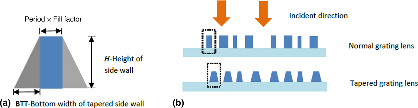
Moth eye is a subwavelength conical structure that is proved to have an enhancement effect on the transmission for high refractive index organic material (moth pupil).[Reference Asadollahbaik, Boden, Charlton, Payne, Cox and Bagnall10] A recent study has mimicked the moth eye with subwavelength tapered structures in a more microscopic scale to achieve giant light extraction for high refractive index devices such as scintillators.[Reference Pignalosa, Liu, Chen and Yi11] Even though the creation of a tapered structure has long been considered as a side effect of reactive ion etching and it is especially common during the etching of subwavelength microlens because a number of nanostructures (phase shifters) with a wide range of dimensions is etched at the same time, recent studies have achieved the controlled modification of a nanotapered structure through reactive ion etching.[Reference Pignalosa, Liu, Chen and Yi11, Reference Saffih, Con, Alshammari, Yavuz and Cui12] To describe the dimension of a tapered nanostructure, the taper ratio b is defined as b = BTT/H, as shown in Fig. 2(a), and a 2D illustration of normal grating lens versus tapered grating lens is shown in Fig. 2(b). Since the nanostructure with a tapered side wall is similar to a diminutive moth-eye structure, will its transmission be enhanced?
(a) Description of a phase shifter structure and taper ratio. (b) Illustration of a 2D cross-section of the normal grating lens and tapered grating lens. Example of one period is specified in dash blocks.

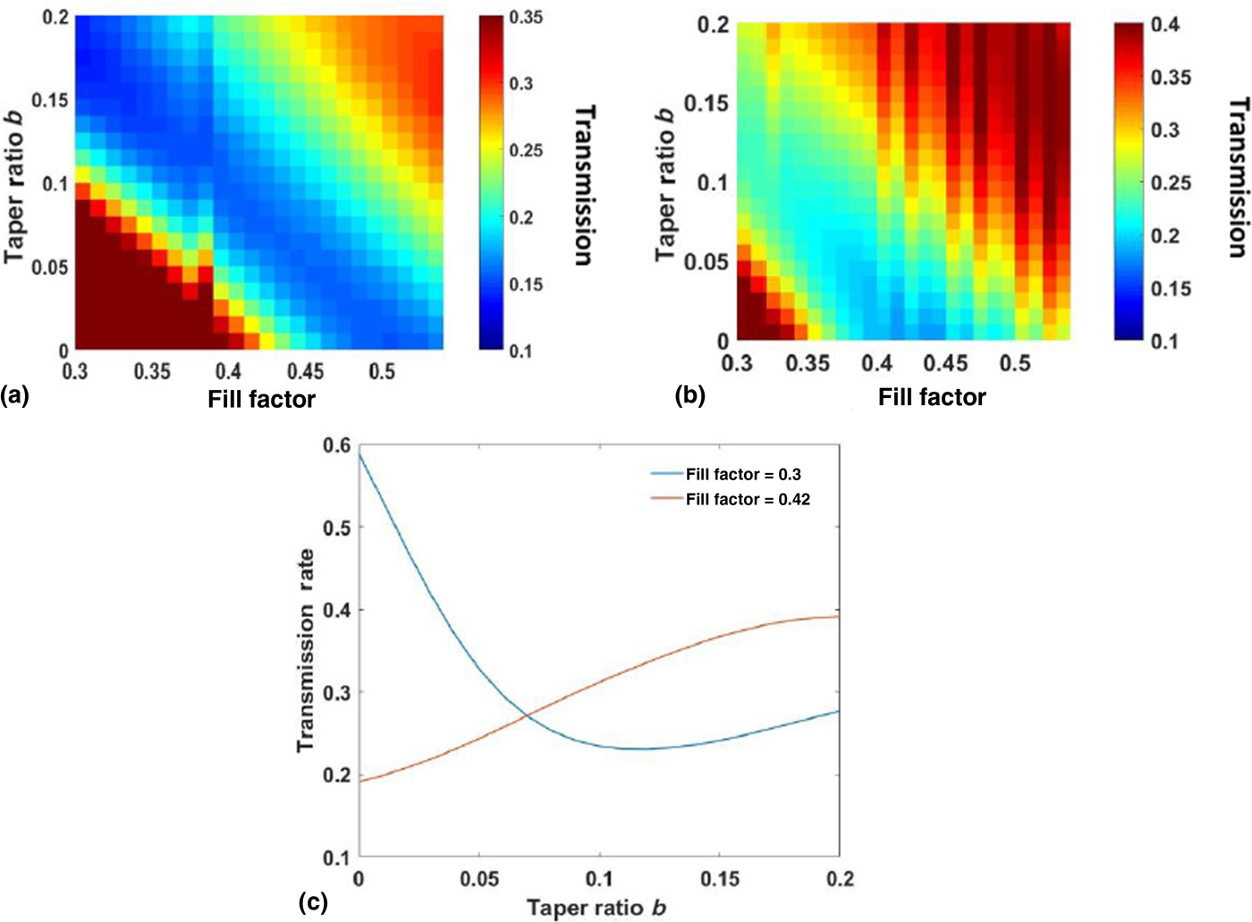
To answer this question, we pick the periods 400 and 450 nm (frequently used when designing microlens) and studied their transmission with varying fill factor and taper ratio, as shown in Fig. 3.
(a) Transmission of the TiO2 phase shifter with a period of 0.4 µm. (b) Transmission of the TiO2 phase shifter with a period of 0.45 µm. (c) Transmission versus taper ratio for phase shifter with a period of 0.45 µm and a fill factor of 0.3 and 0.42, respectively. The thickness of the nanostructures is fixed at 400 nm.

As can be observed in Figs. 3(a) and 3(b), the transmission of a nanostructure varies when its fill factor and taper ratio is altered. With the period of 0.4 µm, for a fill factor below 0.4, the transmission decreases with the increase of taper ratio. For the period of 0.45 µm, the same trend can be found when the fill factor is below 0.35 [Fig. 3(b)]. One example is drawn in Fig. 3(c) as the blue line. This is because for nanostructures with low fill factor, the major area is covered by air and their high transmission mainly results from low material density. The creation of taper structure on low fill factor nanostructures adds a major portion of the material to the original structure. As a result, the blocking effect caused by the addition of taper side wall plays a more significant role compared with the effect of transmission enhancement. On the other hand, for nanostructures with a fill factor larger than 0.45 [Fig. 3(a)], the transmission increases with the increase of taper ratio; and the same trend is found for a fill factor larger than 0.4 with a period of 0.45 µm [Fig. 3(b)]. This indicates that the taper enhancement effect dominates beyond this point (fill factor of 0.45) at the period of 0.4 µm. At this point, we can conclude that the tapered structure has a transmission enhancement effect when the fill factor exceeds a certain threshold. This is because the taper-blocking and taper-enhancement effects together affect the transmission of the tapered subwavelength nanostructure.
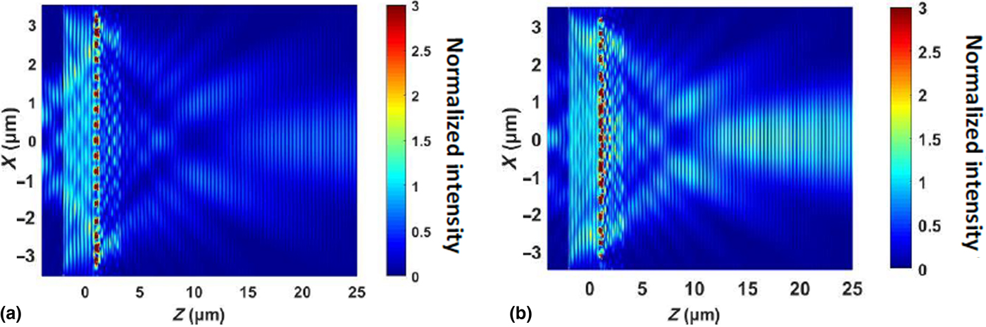
While we can achieve high transmission with high refractive index material (e.g., TiO2) in low fill factor area, we discovered that it is not possible to design a microlens with only low fill factor nanostructures. As mentioned at the beginning, the design of a planar microlens relies on a known phase-matching process, thus enough phase coverage is necessary in order to form a concentrating microlens. As shown in Fig. 1(b), the phase coverage is very small (<40°) for nanostructures with low fill factors (e.g., <0.4) in a range of periods. Furthermore, low fill factor is in another word high aspect ratio, which is challenging for either etching or lift-off process. To acquire enough continuous phase shift with less challenging nanofabrication for TiO2, one group of dimensions is specified in blocks in Figs. 1(b) and 1(d). A microlens with 17 phase shifters (NA = 0.2) is designed within this area whose field distribution is shown in Fig. 4(a) in 2D. The thickness of phase shifters is 400 nm, and the lens is mounted on a glass substrate with a thickness of 2 µm.
(a) Field distribution of normal TiO2 microlens. (b) Field distribution of a “tapered” TiO2 microlens. The intensity is normalized by incident intensity.

As shown in Fig. 4(a), the lens has a very weak focus, this is because most of its phase shifters have very low transmission (0.2–0.3). As a result, reflection becomes dominant, which can also be observed in Fig. 1(d). Instead of being a focusing lens, this lens becomes more of a reflector as the reflected power collected is about 64% of the incident power.
The good news is, based on our study, it is possible that these phase shifters’ transmissions be enhanced through the addition of tapered structure as all phase shifters utilized here show an increase of transmission with the growth of taper ratio.
To test the transmission enhancement of a tapered structure on microlens, a taper side wall [specified as gray in Fig. 2(a)] with b = 0.15 is added to every phase shifter of the microlens presented in Fig. 4(a). The field distribution of a taper-enhanced microlens is shown in Fig. 4(b). As can be observed for the tapered microlens, a focus is formed at approximately the same place with no tapered lens [Fig. 4(a)], while the intensity is increased by ~2.5 times. The reflected power is reduced from ~64% to ~38%, and the focus efficiency with 2 µm width (sensor is placed at the focus point with a width of 2 µm) is increased from 9% to 28%. This shows that the lens’ transmission is significantly enhanced by the tapered structure, which brings huge improvement of its focus property. Another point is one has to be aware that the addition of a tapered structure may bring extra phase shift to a nanostructure, which sometimes causes the significant destructive effect to the focus performance if not designed in the taper-resistant area.[Reference Ye and Yi13] For the design in Fig. 4(b), most of the tapered structure is “taper-resistant,” which means the extra phase introduced by a taper side wall is very small that may not cause a major phase mismatch.
This transmission enhancement effect is crucial for the optimization of subwavelength-grating lens in two aspects. (1) For linearly polarized incidence, considering high refractive index material with certain fill factor is necessary for the sake of large phase coverage, the addition of tapered side wall provides a spike on the phase shifter's transmission. (2) It is shown that the phase shifters with extensively low fill factor (e.g., <0.3) have a high sensitivity to fabrication defects (e.g., tapering), which results a drop of transmission, thus it is necessary to avoid nanostructures of low fill factor as long as the designed phase shifts are covered. In addition, acknowledging the taper transmission enhancement effect, the fabrication process of microlens can be more flexible as the acceptable taper ratio is increased.
Conclusion
In summary, it is numerically demonstrated that a nanoscale tapered structure can enhance the light transmission for phase shifters made from the high refractive material. A subwavelength-grating lens is designed to examine the transmission enhancement effect. As observed, the focus performance can be significantly increased by a tapered structure. This is due to the increased transmission of each independent phase shifter. This result is not only important for the optimization of the planar micrograting lens but also important for the design of micro–nanodiffractive optical devices utilizing materials with high refractive index.
Acknowledgment
The author would like to thank the University of Michigan and Demetra Energy for funding.