I. INTRODUCTION
Polymer dielectrics are an essential component for the realization of flexible field effect transistors (FETs).Reference Ponce Ortiz, Facchetti and Marks1–Reference Sirringhaus3 Common materials used for gate dielectrics in standard FET electronic devices such as SiO2 involve high temperature synthesis and are too brittle to be used in flexible devices. Polymer dielectrics, which can be incorporated into devices at low temperatures and by low cost techniques such as spin coating, offer a viable solution. Furthermore, polymer dielectrics have often shown advantageous effects on the device performances of solution processed organic field-effect transistors (OFETs), where the surface roughness of the dielectric is shown to play a critical role in determining the performance of the OFET.Reference Sirringhaus3 Although many research groups have made significant headway in this area as is highlighted in an insightful and thorough review from the Marks group in 2010,Reference Ponce Ortiz, Facchetti and Marks1 there are still many potential advantages to be explored. Previous examples of flexible dielectrics include poly(methylsilsesquioxane) (PMSQ),Reference Nagase, Hamada, Tomatsu, Yamazaki, Kobayashi, Murakami, Matsukawa and Naito4 poly(2-hydroxyethyl methacrylate) (PHEMA),Reference Yang, Hong, Jang, Chung, An, Choi and Park5 sol-gel silica,Reference Tan, Kulkarni, Cahyadi, Lee, Mhaisalkar, Kasim, Shen and Zhu6 organic capped TiO2 NPs,Reference Cai, Gan, Chan-Park, Bin Yang, Lu, Song, Li and Li Dong7 poly(vinyl alcohol) PVA and poly-4-vinylphenol (PVP) based dielectrics with high-k nanoparticle (NP) fillers BaTiO3Reference Schroeder, Majewski and Grell8,Reference Chon, Ye, Cha, Lee, Koo, Jung and Kwon9 and TiO2.Reference Chen, Chu, He, Yang and Lin10–Reference Yang, Hsu, Hwang and Chang12 There have also been recent developments in the use of supercritical fluids of ZrO2Reference Wei, You, Hendricks, Briseno and Watkins13 or incorporation of ZrO2 NPsReference Zirkl, Haase, Fian, Schön, Sommer, Jakopic, Leising, Stadlober, Graz, Gaar, Schwödiauer, Bauer-Gogonea and Bauer14–Reference Lee, Jeong and Moon16 for high-κ inorganic/organic composites. Even silk protein has been cleverly utilized as a dielectric material.Reference Wang, Hsieh and Hwang17 Most of these methods require a great deal of skill in chemical fabrication methods and can be tricky and difficult to reproduce for physicists and engineers who are not adequately trained in complex chemical synthesis routes. In this work we have developed a simple synthesis route for PMSQ loaded with MgO NPs, using a heated ultrasonic bath to mix with materials. The MgO NPs were incorporated into the synthesis of PMSQ based dielectrics to increase the dielectric constant of the material. We found that the PMSQ + MgO NP composite materials have similar spin-coating processing properties compared to the standard PMSQ, making this method extremely advantageous by the ease of reproducibility. Here, the dielectric constant is found to increase from 2.8 for raw PMSQ alone up to 3.4 for PMSQ + MgO NP composites loaded with 0.39 wt% of MgO, similar to κ = 3.9 for SiO2. To further increase the dielectric constant, PMSQ + TiO2 NP composite materials are also synthesized and tested. However the PMSQ + TiO2 NP materials were found to be unsuitable for device fabrication methods required to produce OFETs and other flexible electronic FETs. In this work, we describe the synthesis of PMSQ + MgO NPs via a simple route and show the successful application of this material as a dielectric layer for organic FETs. A PMSQ + MgO dielectric layer is compared to an SiO2 film as a functioning dielectric in a poly(3-hexylthiophene) (P3HT) OFET and is shown to have a similar device performance for our optimized devices.
II. EXPERIMENTAL METHODS
Poly(methylsilsequioxane) (PMSQ) NP composites are fabricated by adapting a method previously used by Ooi et al.,Reference Ooi, Ahmad, Aw, Gao and Travas-Sejdic18 for nonvolatile memory devices. To begin, the precursors trimethoxymethylsilane (MTS), butanol (n-BuOH) and deionized water are mixed at a volume ratio of 4:10:1. To incorporate, MgO NPs (Aldrich product 549649 NP sizes < 50 nm, Sigma-Aldrich Corporation, St. Louis, MO) are weighed out directly into the vial before adding the MTS, n-BuOH and DI water. The solutions are then sonicated for 6 or 8 h at 60 °C in a heated ultrasonic bath. After this, the solutions are left to age for varying lengths of time, ranging from 1 day to 1 week. The weight percentages of the MgO NPs were varied for 3 sets of samples with MgO-1 = 0.096%, MgO-2 = 0.29%, and MgO-3 = 0.386% respectively, see Table I. A further sample was made using identical methods with a 0.096% weight of TiO2 (DeGuassa P25 NPs ≈ 25 nm), TiO2-1. To investigate the structural properties of the PMSQ, Fourier transform infrared spectroscopy (FTIR) is performed using a Bruker Tensor 27 spectrometer (Bruker Corporation, Billerica, MA) in an attenuated total reflection (ATR) geometry. For all samples 1 drop of solution is placed on the diamond.
The wt% of MgO NPs loaded into the PMSQ composite materials with the resulting dielectric constants and calculated volume fractions.

To characterize the dielectric performance of our films, parallel plate capacitors are fabricated, where a highly doped silicon substrate (Si++ = 0.005 ohm cm) acts as the bottom electrode and a thin film of gold is deposited as the top contact. The dielectric layer of PMSQ or PMSQ + MgO NPs, mixed for 8 h, is deposited directly onto a clean silicon substrate by spin coating at 2000 rpm for 60 s. The top 50 nm thick gold contact was then deposited by thermal evaporation through a precision fabricated shadow mask from Osilla (Ossila Ltd, Sheffield, UK), with contact areas 2 × 4 mm. The capacitors were then characterized using an Agilent 4249A impedance analyzer (Agilent, Santa Clara, CA) using a purpose designed rig capable of coming into contact with our samples. The rig was calibrated using a commercially available capacitor and the setup was further tested using identically doped Si++/SiO2 (100 nm oxide thickness) samples with identical contact geometry to the PMSQ capacitors. The SiO2 layer was found to have a dielectric constant of 3.9, with high precision due to the use of the precise shadow mask, showing that the rig and electrode geometry was suitable for these measurements. The PMSQ and the PMSQ + MgO NP film thicknesses were measured by making scratches in the films and measuring the step height with a Veeco Dektak profilometer (Veeco, Plainview, NY) postimpedance measurements. Scanning electron microscopy (SEM) has also been used on the films, using an FEI NovaNanoSEM (FEI Company, Hillsboro, OR).
The OFETs performance is then investigated with the PMSQ + MgO NP dielectric films as the gate insulator region of the device. The semiconducting channel was made using poly(3-hexylthiophene) (P3HT) (American Dye Source Inc., ADS306PT, Baie D'Urfe, Quebec, Canada), a commonly used spin processable semiconductor for OFETs and organic photovoltaics, using a 10 mg/mL solution of P3HT in chloroform. The processing of the OFET is similar to the fabrication of the capacitors. To begin, a highly doped Si wafer (0.005 ohm cm) is cleaned and the PMSQ + MgO NP composite is spin coated at 2000 rpm for 60 s before annealing the films on a hotplate at 150 °C for 2 h. The P3HT semiconducting layer was then spin-coated at 2500 rpm for 40 s directly onto the annealed PMSQ + MgO NP layers. No P3HT annealing step was performed. A control sample was made with a Si/SiO2 substrate, whereby the P3HT layer was coated directly onto the clean SiO2 surface. The samples were then loaded into the Angstrom Engineering thermal evaporator (Angstrom Engineering, Kitchener, Ontario, Canada), where we deposited 50-nm thick gold contacts through an Osilla OFET shadow mask, see Fig. 1(a). The contact lengths are 4 mm and the inter-digitated channel widths are 40 μm. The devices were then tested in a field effect geometry using an Agilent 4156 C semiconductor parameter analyzer (Agilent, Santa Clara, CA) and a Rucker and Kolls probe station.
A schematic representation of the fabrication process for organic FETs. (a) A clean SiO2/Si substrate or Si substrates coated with PMSQ + MgO NP dielectric are initially prepared. P3HT is then directly spin coated onto the dielectric layer. Top contacts of 50 nm Au are then deposited by thermal evaporation through an Osilla FET shadow mask. (b) A clean SiO2/Si substrate is coated with 3/50 nm Cr/Au back gate electrodes by thermal evaporation through an Osilla gate electrode shadow mask. The PMSQ + MgO NP dielectrics are then spin coated and annealed directly above the gate electrodes. P3HT is then spin-coated before top contacts of 50 nm Au are deposited by thermal evaporation through an Osilla FET shadow mask. Due to the design of the shadow mask, the gate electrode aligns with the OFET channel. The channel lengths are 40 μm for all devices.

Further device experiments were done with PMSQ + MgO NP composite dielectrics, mixed for 6 h, with a slightly different device fabrication procedure being used, Fig. 1(b). Si/SiO2 substrates were cleaned and a back gate electrode was fabricated using the Osilla OFET back gate shadow mask. The contacts were fabricated in the Angstrom Engineering thermal evaporator, with Cr/Au 3/50 nm film thicknesses. The samples were then cleaned in acetone and IPA prior to being coated with PMSQ + MgO NP dielectrics, as described above. The P3HT layers were then deposited by spin coating at 2500 rpm for 40 s before being loaded into the evaporator and depositing 50 nm thick Au contacts using the Osilla FET mask, which aligns to the bottom gate electrode, see Fig. 1(b). A control sample with the standard Si/SiO2/P3HT OFET geometry was also made in parallel.
III. RESULTS AND DISCUSSION
A. Preparation and characterization of PMSQ + MgO composites
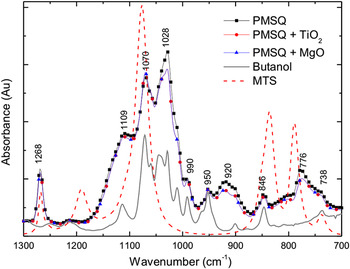
In the first instance, we have fabricated PMSQ, PMSQ + MgO-1 NPs and PMSQ + TiO2-1 by mixing in an ultrasonic bath at 60 °C for 8 h. The solutions were characterized using FTIR analysis in ATR geometry shown in Fig. 2, which presents the spectra for PMSQ (black squares), PMSQ + MgO NPs (red circles) and PMSQ + TiO2 NPs (blue triangles), along with n-BuOH (gray line) and MTS (dashed line), which are shown for comparison. The spectra show evidence of the PMSQ formation for the PMSQ and the PMSQ + NP samples, with small peaks at 920 and 776 cm−1 both being identified as PMSQReference Chuang, Sheen, Wei, Teng, Yen and Ma19 and larger peaks at 1268, 1109, and 1028 cm−1 which are not merely residual MTS and n-BuOH. The peaks at 1268 and 776 cm−1 represent the stretching vibrations of the Si–C from Si–CH3 group,Reference Chuang, Sheen, Wei, Teng, Yen and Ma19 with the sharp peak at 1268 cm−1 specifically indicating the presence of methyl group –CH3 for either MTS or PMSQ.Reference Chuang, Sheen, Wei, Teng, Yen and Ma19–Reference Liu, Xu, Li, Li, Ma and Zhang22 The peaks at 1109 and 1028 cm−1 represent the symmetrical and asymmetrical Si–O–Si backbone of PMSQ stretching vibrations respectivelyReference Chuang, Sheen, Wei, Teng, Yen and Ma19–Reference Liu, Xu, Li, Li, Ma and Zhang22 and indicate a branched ladder-like structure of PMSQ.Reference Chuang, Sheen, Wei, Teng, Yen and Ma19,Reference Chuang, Sheen, Wei, Teng, Yen and Ma20 Altogether, with the broad peak at 920 cm−1 from the Si–OH vibrations from PMSQReference Chuang, Sheen, Wei, Teng, Yen and Ma19–Reference Liu, Xu, Li, Li, Ma and Zhang22 and the presence of Si–O–Si, Si–OH and Si–CH3 characteristic peaks, the FTIR spectra clearly support the successful formation of a PMSQ polymer by this method. However, the relatively high intensity of the siloxane (Si–O–Si) peak at 1028 cm−1 compared with the peaks associated with a more ordered PMSQ at 1109 and 1070 cm−1 imply a lack of order in the polymer,Reference Chuang, Sheen, Wei, Teng, Yen and Ma19,Reference Chuang, Sheen, Wei, Teng, Yen and Ma20,Reference Liu, Xu, Li, Li, Ma and Zhang22 with the peak at 1070 cm−1 being directly attributed to an irregular/random network of PMSQ.Reference Chuang, Sheen, Wei, Teng, Yen and Ma19,Reference Chuang, Sheen, Wei, Teng, Yen and Ma20 As these spectra are taken only in the solution phase and not after the spin coating and annealing stage that our PMSQ and PMSQ + NPs would go through for device performance, we can only speculate on the final ordering of the PMSQ post anneal. It is possible that the thin films would show a more ordered structure upon thermal annealing as shown by other groups, with further cross-linking taking place and spatial confinement of the polymer due to the spin coating.Reference Nagase, Hamada, Tomatsu, Yamazaki, Kobayashi, Murakami, Matsukawa and Naito4,Reference Chuang, Sheen, Wei, Teng, Yen and Ma19,Reference Chuang, Sheen, Wei, Teng, Yen and Ma20,Reference Xiang, Zhang, Wang, Yu, Long, Zhang, Zhao and Xu23
FTIR spectra of the PMSQ (black squares), PMSQ + MgO NPs (red circles) and PMSQ + TiO2 NPs (blue triangles), along with n-BuOH (gray line) and MTS (dashed line).

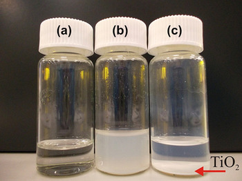
In the original work by OO et al.,Reference Ooi, Ahmad, Aw, Gao and Travas-Sejdic18 the PMSQ was left to age for 1 week prior to device fabrication. In the case of our PMSQ + MgO NPs, mixing the polymer in the vial for 8 h leads to the solution setting solid over the course of 48 h. Although the PMSQ and the PMSQ + NPs solutions all appeared similar to each other by FTIR analysis, immediately after cooling post synthesis, there is a visible difference between the raw PMSQ and the MgO loaded PMSQ and the PMSQ with TiO2. Shown in Fig. 3 is a photograph of the PMSQ vials after 2 days. The TiO2 loaded PMSQ does not maintain a uniform suspension after aging and the NPs appear to sink to the bottom of the vial. In contrast, the PMSQ + MgO NPs maintain an even suspension before setting solid. It is reasonable to assume that the MgO NPs are fully included in the PMSQ structure whereas the TiO2 are merely weekly suspended. Further evidence is in the setting of the solution in the vials, where the PMSQ + MgO NP suspensions form a solid gel at room temperature in the vial after several days. This shorter shelf-life can be attributed to the MgO NPs accelerating the aging of the polymer and may be due to an increase in the cross-linking, similar to other organic-inorganic hybrid materials.Reference Xiang, Zhang, Wang, Yu, Long, Zhang, Zhao and Xu23
A photograph of (a) PMSQ, (b) PMSQ + MgO-1 and (c) PMSQ + TiO2-1. The red arrow on (c) indicates the region of TiO2 NPs, which have sunk to the bottom of the vial.

To study the dielectric performance of the PMSQ and PMSQ + MgO NP films, sandwich electrode structures are fabricated as described in the experimental section. In the first instance, all samples were spin coated onto clean Si substrates at 2000 rpm for 60 s. The PMSQ and PMSQ + MgO NPs produced films with uniform appearance to the naked eye. In stark contrast, the PMSQ + TiO2 NP films looked rough to the naked eye and the resulting thicknesses were too low to accurately measure with the Dektak at approximately 25 nm. This is also the average size of the TiO2 NPs, indicating a poor suspension of TiO2 NPs in the polymer solution, which prevents good spin-coating. The PMSQ + TiO2-1 solution is no longer considered, as although the high dielectric constant of TiO2 is appealing for device applications, the lack of evidence for NP incorporation into the polymer matrix makes the material unsuitable. In contrast, the PMSQ and the PMSQ + MgO NP films were uniform and showed good capacitive behavior over a wide range of frequencies. The dielectric constant of the films can then be established from the impedance analyser by considering the relationship among dielectric constant (κ), capacitance (C) and the thickness of the film (d).
 $$\kappa = {{Cd} \over {{\rm{\varepsilon }}_0 A}}\quad,$$
where ε0 is the permittivity of free space and A is the area of the contact. The dielectric constant of the films, as a function of frequency out to 2 MHz, is shown in Fig. 4 alongside the dielectric constant of the SiO2 control sample. The dielectric constant of the SiO2 is found to be 3.9, verifying the calibration of the purpose-made rig. The dielectric constant of PMSQ was measured as 2.8, which is consistent with other work in the literature.Reference Xi, He, Xu, Ge, Meng, Jia and Yu24,Reference Ro, Kim, Theato, Gidley and Yoon25 The PMSQ + MgO NPs show a rising dielectric constant with increasing weight of added NPs, from MgO-1 = 2.9, MgO-2 = 3.2, and MgO-3 = 3.4, Fig. 4. We observed that the PMSQ + MgO NP films were extremely thick (1.8–2 μm), whereas the PMSQ films were around 750 nm coated under the same spin conditions. The PMSQ + MgO NP solutions were all highly viscous in comparison to PMSQ and, as discussed above, have a shorter shelf life. Therefore it was unsurprising that the films were considerably thicker. Additionally, the PMSQ and the PMSQ + MgO NPs were not 100% uniform as observed from Dektak profiling and several thickness measurements were made to determine the value of d to be used to calculate k. Care was taken to minimize the errors in the final value of k. There is clearly a need to fully investigate the surfaces of these films ideally with a high precision technique such as atomic force microscopy.
The dielectric constant of SiO2 (squares), PMSQ (circles), PMSQ + MgO-1 (upright triangle), PMSQ + MgO-2 (downward triangle) and PMSQ + MgO-3 (diamond), taken out to 2 MHz. Inset: The volume fraction of the MgO as calculated from the dielectric constants using the Maxwell-Garnett formula compared to the volume fraction of MgO as a percentage of the weight of the solution.

The percentage weight of NPs added initially was MgO-1 = 0.098%, MgO-2 = 0.29%, and MgO-3 = 0.39%; however during the heating and mixing stage, some of the solvent was evaporated off, resulting in a higher percentage weight of the NPs in the final solution. The NPs weight fractions, post 8 h mixing, were MgO-1 = 0.11%, MgO-2 = 0.32%, and MgO-3 = 0.44%, Table I. As the wt% is increased, the dielectric constant increases as expected. However, it is not yet known where the maximum loading point will lie, and it should be possible to further increase the wt% of MgO. If we were to assume that the NPs uniformly fill the PMSQ background as spherical particles,Reference Petrovsky, Manohar and Dogan26 we can make use of the Maxwell-Garnett formula,Reference Garnett27Eq. (2), where, εeff is the effective dielectric constant of the composite material, ε1 is the dielectric constant of the uniform spheres, here MgO is taken to be 9.8, and ε2 is the dielectric constant of the background material, in which case PMSQ = 2.8.
 $${{{\rm{\varepsilon }}_{{\rm{eff}}} - {\rm{\varepsilon }}_{\rm{2}} } \over {{\rm{\varepsilon }}_{{\rm{eff}}} \,{\rm{ + \,2\varepsilon }}_{\rm{2}} }} = x_1 {{{\rm{\varepsilon }}_{\rm{1}} {\rm{ - \,\varepsilon }}_{\rm{2}} } \over {{\rm{\varepsilon }}_{\rm{1}} \,{\rm{ + \,2\varepsilon }}_{\rm{2}} }}\quad.$$
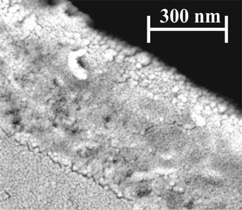
The remaining component of the Maxwell-Garnett formula is χ1, which is the volume fraction of the spheres. By taking the density of PMSQ to be 1.3 g/cm3 and MgO as 3.58 g/cm3, we can compare the volume fraction of MgO as a percentage of the weight of the solution and compare directly to the volume fraction of the MgO as calculated from the dielectric constants using the Maxwell-Granett formula,Reference Petrovsky, Manohar and Dogan26 shown in the inset of Fig. 4. Here we calculate volume fractions from the wt% of MgO as MgO-1 = 0.039, MgO-2 = 0.116, MgO-3 = 0.159, and via the Maxwell-Garnett method as MgO-1 = 0.025, MgO-2 = 0.1, and MgO-3 = 0.146 (see Table I). There is no reason to assume that the entire % weight of NPs would be equal to the volume fraction of the NPs in the dielectric media. The process of the initial polymer synthesis and mixing, as well as the process of spin coating the polymers, could have resulted in an unknown volume fraction of MgO. However, as we assume our measured dielectric constants to be correct and we find strong agreement from the calculated volume fraction and the measured volume fractions of these films, we can predict that the distribution of the NPs is highly uniform due to good initial mixing of the solutions. Further structural analysis of the as-spun films is ideal to verify these packing fractions, and to confirm that the MgO NPs do form uniform spheres within the PMSQ matrix. Figure 5 shows a backscattered SEM image of a cross-section of a film of PMSQ + MgO-3 mixed for 6 h and spun at 2000 rpm onto Si. The films are cleaved using a diamond pen and coated with the metal immediately prior to loading into the SEM. Imaging these insulating films is a challenge as there is little contrast on the sample surface and exposure to the beam damages the delicate polymer material which forms the bulk of the film. As can be seen in the image, the PMSQ + MgO-3 films are highly uniform and there is no strong evidence of NP clumping. Altogether the presented data are strong evidence of the uniformity of the films and hence their suitability for device applications.
A backscattered SEM image of a PMSQ + MgO-3 film mixed for 6 h and spin coated at 2000 rpm.

B. Application of PMSQ + MgO composites in OFETs
The main thrust of this work is to determine whether the PMSQ + MgO NP films function as the dielectric layers in transistors. In addition to the fabrication of the parallel plate capacitors, organic FETs are fabricated using P3HT dissolved in chloroform as the conducting channel. In Fig. 6, the output characteristics are shown for the devices, which were fabricated in the process shown in Fig. 1(a). Figure 6 shows the resulting transfer characteristic of P3HT transistors made on PMSQ + MgO-1, MgO-2, and MgO-3 in comparison to a control device made in the same batch with a SiO2 thickness of 300 nm. The devices with the PMSQ + MgO NP dielectric devices show significantly less gate voltage dependence than the SiO2 sample, however this is unsurprising given that the thickness of the SiO2 is 300 nm while the thickness of the PMSQ + MgO NP films approached 2 μm (as measured by Dektak). Importantly, it has been shown that the device fabrication procedure is compatible with the PMSQ + MgO NP material.
The transfer characteristics of OFETs fabricated on various dielectrics, including 300 nm SiO2, PMSQ + MgO-1, PMSQ + MgO-2 and PMSQ + MgO-3. The source drain voltage is −20 V for all devices.

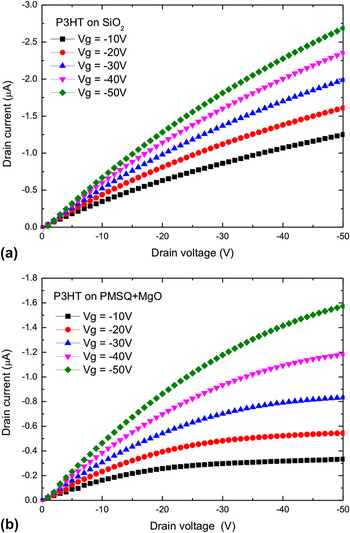
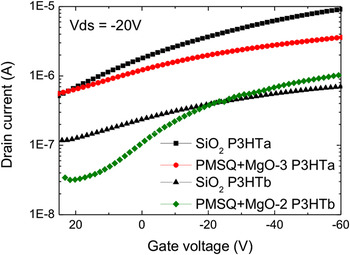
To optimize the performance of PMSQ + MgO NP composite films as dielectric films for OFETs, efforts have been made to reduce the final film thicknesses, by reducing the mixing time in the ultrasonic bath down to 6 h. This has produced PMSQ + MgO-2 and -3 NP films with thicknesses of 600–800 nm (measured by dektak), which is comparable to the pristine PMSQ. Shown are the output characteristics of a P3HT device on 300 nm SiO2 [Fig. 7(a)] and for a P3HT device with PMSQ + MgO-2 [Fig. 7(b)], the latter using the device fabrication scheme described in Fig. 1(b). All of our devices are fabricated and measured in air and no P3HT annealing step has been carried out. The current is higher in the SiO2 control sample in comparison to the PMSQ + MgO-2 NP dielectric device at a given Vds, and the polymer dielectric material shows signs of saturation at around −30 V Vg. In Fig. 8, the transfer characteristics of the P3HT on SiO2 control samples are shown alongside P3HT on PMSQ + MgO-2 and another optimized sample with PMSQ + MgO-3 NPs, both being held at −20 V Vds. There are two separate SiO2 control samples to indicate different batches of P3HT indicated as P3HTa and P3HTb on the graph respectively. All devices show clear p-type FET behavior, however, the device with the PMSQ + MgO-2 NP dielectric has the best performance, with the off current in the range of 10 s of nanoamps. The off current shown for the SiO2 dielectric control sample from the same batch of P3HT is one order of magnitude higher. As our devices are made and characterized in air, it is only meaningful to compare devices against each other from P3HT dissolved on the same day. Our OFET devices do not outperform the current state of the art in OFETsReference Sirringhaus3,Reference Tan, Kulkarni, Cahyadi, Lee, Mhaisalkar, Kasim, Shen and Zhu6,Reference Park, Kim, Graham and Reichmanis28,Reference Reséndiz, Estrada, Cerdeira, Iñiguez and Deen29 and the OFET device behavior could be improved by fabricating thinner P3HT layersReference Wei, You, Hendricks, Briseno and Watkins13,Reference Park, Kim, Graham and Reichmanis28,Reference Reséndiz, Estrada, Cerdeira, Iñiguez and Deen29 and use of a glovebox for sample preparation and measurements.Reference Ponce Ortiz, Facchetti and Marks1,Reference Sirringhaus3,Reference Pretl, Kroupa, Hamáček, Džugan, Řeboun and Čengery30 The use of PVP TiO2 NP dielectrics for P3HT channel devices had previously shown enhanced OFET performance, similar to our devices,Reference Yang, Hsu, Hwang and Chang12 however those devices used a different geometry with a top gate effectively encapsulating the P3HT layer and avoiding further water contamination during the measurements in atmosphere. They therefore achieved higher on currents. Switching to other channel materials, such as higher molecular weight P3HTReference Park, Kim, Graham and Reichmanis28 or an evaporated channel material such as pentacene,Reference Sirringhaus3,Reference Tan, Kulkarni, Cahyadi, Lee, Mhaisalkar, Kasim, Shen and Zhu6,Reference Chen, Chu, He, Yang and Lin10,Reference Wang, Hsieh and Hwang17 should also be compatible with this material. Our best bottom gate devices using PMSQ + MgO-2 P3HTb with no encapsulation compare well to those produced with an exposed pentacene channel and a 650 nm thick TiO2 NP film.Reference Cai, Gan, Chan-Park, Bin Yang, Lu, Song, Li and Li Dong7 As we suffer from extreme variability in our devices due to processing constraints, it would be useful to test these materials as dielectrics for more air stable channel materials such as carbon nanotubes or inorganic nanowire devices for flexible electronics.
The output characteristics of (a) a P3HT OFET on 300 nm SiO2 dielectric, and (b) on 700 nm thick PMSQ + MgO-2 NP dielectric at various gate voltages.

The transfer characteristics of P3HT devices with batch a, 300 nm SiO2 (squares) and PMSQ + MgO-3 NPs (circles), and batch b, 300 nm SiO2 (triangles) and PMSQ + MgO-2 NPs (diamonds). The source drain voltage is −20 V for all devices.

IV. CONCLUSION
The advantage of the PMSQ + MgO NP materials is in the ease of processing and the simplicity of the NP incorporation to raise the dielectric constant of the PMSQ material from 2.8 to 3.4. There is still the need to develop a fuller understanding of the processes during the mixing phase and the effects of the spin coating on the structure of the composite films. We have shown the PMSQ + MgO NP material to have robust processing compatible with solution processed P3HT OFETs.
ACKNOWLEDGMENTS
N. Plank would like to thank the FRST postdoctoral fellowship scheme, project number E1558 for funding. H. Zheng thanks the Victoria University and the Chinese Government joint Scholarship Scheme for Ph.D funding and S. Agarwal and N. Plank thank the Marsden fund, project number E1728. N. Plank would like to thank Dr. Ruth Knibbe of Industrial Research Limited for access to and training on the NovaNanoSEM.