Introduction
Owing to their outstanding electrical properties,[Reference Javey, Kim, Brink, Wang, Ural, Guo, McIntyre, McEuen, Lundstrom and Dai1, Reference Yao, Kane and Dekker2] single wall carbon nanotubes (SWNTs) have shown great potential in various electrical devices such as thin film transistors (TFTs), logic circuits (semiconducting), electrical interconnects, and transparent electrodes (metallic).[Reference Tans, Verschueren and Dekker3–Reference Wu, Chen, Du, Logan, Sippel, Nikolou, Kamaras, Reynolds, Tanner, Hebard and Rinzler6] TFTs made of SWNTs look especially promising. The non-uniform chirality of individual SWNTs, however, is an obstacle for uniform electrical properties along with short junctions and high contact resistance.[Reference Xu, Chen, Hu and Zhitenev7]
In recent years, two distinctive surface-assisted growth modes, serpentine[Reference Geblinger, Ismach and Joselevich8] and parallel growth,[Reference Kocabas, Hur, Gaur, Meitl, Shim and Rogers9,10] have been developed for SWNT alignment to prevent cross contacting between nanotubes. These two growth modes, depending on the flow direction of the carbon feed gas relative to the orientation of the atomic step edge of substrates, enable the fabrication of homogeneous SWNTs of the same type between two electrodes, and also provide a parallel array of SWNTs establishing multiple transport pathways. However, these methods do not concurrently provide the control over the density and the chirality of SWNTs on the channel of TFT. The high-density and purely semiconducting SWNTs are essential to make the electrical properties of SWNT-based TFTs statistically uniform.
Another issue related to SWNT-based electronic devices is the high contact resistance.[Reference Hu, Hecht and Grüner11–Reference Franklin and Chen13] Ohmic contacts in SWNT devices can lead to highly efficient device performance. Recently, Chen et al.[Reference Chen, Appenzeller, Knoch, Lin and Avouris14] reported reduced contact resistance by choosing metals with similar work functions as that of SWNTs. On the contrary, Woo et al.[Reference Woo, Duesberg and Roth15] demonstrated low contact resistance of SWNTs on a Pd electrode using a local point annealing method. However, these methods are difficult to implement because of the limitations in adapting the work function between two intrinsically different materials. Besides this attempt for reducing contact resistance, a fabrication method using carbon contacts of the SWNTs and multi-walled carbon nanotubes originated from the same graphene structure was reported.[Reference Austing, Lefebvre, Bond and Finnie16] In that sense, an all-SWNT device that uses the same material at both the source/drain electrode and channel is attractive not only because it offers low contact resistance, but also because it can operate as a highly transparent device.
Here we propose a simple process to simultaneously fabricate the electrodes and channel of a TFT device with SWNTs. In this process, the well-aligned SWNTs are grown as the channel material, whereas the network-type SWNTs are grown as source/drain electrodes. Although several groups have demonstrated all-SWNT-based TFTs by various methods,[Reference Hong, Du, Lan, Kim, Kim and Rogers17–Reference Jang, Jang, Lee, Suh, Baik, Hong and Ahn19] none have reported the simultaneous fabrication of SWNT channel and electrodes. The contact resistance between well-aligned SWNTs and network-type SWNTs is measured at various channel lengths and densities. The all-SWNT TFTs, as composed by simultaneous grown SWNTs, show low contact resistance (3.3 kΩ) and high mobility (161 cm2/V s). Moreover, it avoids the formation of residues caused by multiple transfer processes.[Reference Cao, Zhu, Lemaitre, Xia, Shim and Rogers18–Reference Cao, Hur, Zhu, Sun, Wang, Meitl, Shim and Rogers20] The all-SWNT TFTs are then transferred onto a transparent substrate where they demonstrate 80% transmittance in the visible wavelength range.
Results and discussion
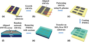
Figure 1 illustrates the overall fabrication process of the all-SWNT TFT. A detailed description for the fabrication process is given in the Experimental section and Supplementary material. During the CVD growth process, highly aligned SWNTs and network-type SWNTs are simultaneously grown in two regions: the aligned SWNTs in between the patterned Fe catalyst lines and the network-type SWNTs in the catalyst-patterned area [Figs. 1(a) and 1(b)]. To obtain a high density of SWNTs, the deposition rate of Fe was fixed below 3 Å/min. By controlling the growth conditions, the density of aligned SWNTs and network-type SWNTs could be varied from 0.65 to 2.5 and 19 to 32.5 SWNTs/μm, respectively. After patterning the SWNT device into smaller-sized units [Fig. 1(c)], the sample was transferred to a target substrate [Figs. 1(d) and 1(e)]. Finally, the transferred TFTs were subjected to an electrical breakdown process to selectively remove the metallic SWNTs in the channel region by applying a high voltage across the electrodes [Fig. 1(f)]. Owing to the execution of electrical breakdown process, Au was deposited on network-type SWNT electrodes to prevent oxidation and electrical burning of network-type SWNTs. After electrically removing metallic SWNTs in the channel, the Au was dissolved away by etchant (Fig. S1).
The fabrication procedures of an all-SWNT TFT: (a) preparation of patterned regions of Fe catalysts, (b) simultaneous growth of aligned and network-type SWNTs, (c) device isolation using O2 plasma, and (d–f) transfer process from quartz to SiO2/Si substrate.

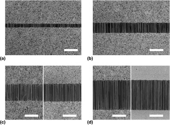
Figures 2(a)–2(d) show scanning electron microscope (SEM) images of four representative channel lengths from 0.5 to 48 µm comprising aligned SWNTs between network-type SWNT electrodes. These samples were all transferred onto an SiO2/Si substrate prior to imaging. In all images, the boundary between the electrodes made of network-type SWNTs (top and bottom) and the channel consisting of horizontally aligned SWNTs (middle) can clearly be identified. The density of aligned SWNTs can be controlled from ~1 SWNTs/μm [Fig. 2(c), left] to ~2.5 SWNTs/μm [Fig. 2(c), right]. Minimal cross linking among individual SWNTs in the channel is observed. Figure 2(d) presents images of network-type SWNTs showing two different densities (~19 SWNTs/μm: left, ~32.5 SWNTs/μm: right) in the electrodes.
SEM images of all-SWNT TFTs with different channel lengths and SWNT densities: (a) device with channel length of 8 µm and electrode density of ~19 SWNT/μm, (b) channel length of 12 µm and electrode density of ~19 SWNT/μm, (c) channel length of 20 µm and electrode density of ~1 SWNTs/μm (left) and ~2.5 SWNTs/μm (right), and (d) channel length of 48 µm and electrode density of ~19 SWNTs/μm (left) and ~32.5 SWNTs/μm (right). Scale bars are 20 µm.

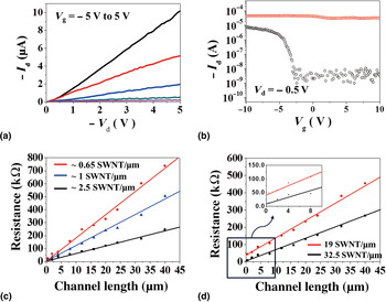
Figure 3(a) shows I–V curves measured for different gate biases (V g) from an all-SWNT TFT device after electrical breakdown. The source–drain current (I d) at V d = −5 V is 10 nA (V g = 5 V), which is four orders less current level compared with 200 µA observed before electrical breakdown. Also, I–V curves show the saturation behaviors in high bias (Fig. S2). A terraced drop of I d during the breakdown process was observed, suggesting that the metallic SWNTs become disconnected. However, the semiconducting SWNTs were also affected through the additional breakdown processes. I/V curve dependent on gate bias shows p-type behavior. This corresponds to the previous showing the p-type carbon nanotube field effect transistors without any doping.[Reference Tans, Verschueren and Dekker3, Reference Martel, Schmidt, Shea, Hertel and Avouris21, Reference Cui, Freitag, Martel, Brus and Avouris22] From the transfer curves [Fig. 3(b)], the on/off ratio after electrical breakdown was shown to be enhanced from 1.5 to 2410 and the field-effect mobility was about 161 cm2/V s which is consistent with previous results.[Reference Cao, Zhu, Lemaitre, Xia, Shim and Rogers18–Reference Cao, Hur, Zhu, Sun, Wang, Meitl, Shim and Rogers20]
(a) I–V characteristics of the all-SWNT TFT after electrical breakdown. Channel length and width is 12 and 100 µm, respectively. The density of SWNTs in channel and electrodes is ~2.5 and ~32.5 SWNTs/μm, respectively. (b) Transfer curve before (red) and after (black) the electrical breakdown at (a). The V d was −0.5 V. (c) On-state resistance as a function of channel length for aligned SWNT densities of 0.65 (red), 1 (blue), and 2.5 (black) SWNTs/μm. (d) On-state resistance as a function of channel length for network-type SWNT densities of ~19 SWNTs/μm (red) and ~32.5 SWNTs/μm (black). Inset shows the extrapolated resistance near zero channel length.

From the three different SWNT density groups of all-SWNT TFT devices [Figs. 2(c) and 2(d)], the channel resistances were measured according to the varying channel distance and shown in Fig. 3(c). As the density of SWNTs in the channel is increased from 0.65 to 2.5 SWNTs/μm, the slope of the linear fit of channel resistance is reduced. This means that the higher channel density of SWNTs can enhance the electrical performance of all-SWNT TFT. It is valuable to note that in all three different SWNT density groups the intercept points on the resistance axis were not changed. This implies that the data of our devices can be analyzed using a parallel circuit model. Based on the parallel circuit theory and the resistance variance along with the channel density and distance, an effective density of SWNTs in the channel at the density of 2.5 SWNTs/μm is evaluated to be ~0.28 SWNTs/μm after electrical breakdown. This suggests the need for more studies for the increment of the effective SWNT density on the channel to improve the electrical performance. Figure 3(d) shows the dependence of the total resistance on the density of the network-type SWNTs. As the SWNT density increases from 19 to 32.5 SWNTs/μm, the resistance decreases fivefold which might be due to the lower electrode resistance and more connections between network-type SWNTs and channel SWNTs. The network-type SWNTs in source/drain region showed a sheet resistance of 14 ± 0.8 kΩ/sq at a density of 32.5 SWNTs/μm and 49 ± 1.2 kΩ/sq at a density of 19 SWNTs/μm. This result implies that the current level of the device can be increased through increasing the density of SWNTs on both electrodes and channel.
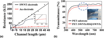
Figure 4(a) shows the comparison of the on-state resistance as a function of channel length measured from an all-SWNT TFT and a SWNT TFT without having applied electrical breakdown. From the intercept of the Y-axis shown in the inset, the contact resistance in the all-SWNT TFT is estimated to be ~3.3 kΩ, whereas in the conventional SWNT TFT it is ~7.6 kΩ. This result suggests that the all-SWNT TFT devices should have a significantly lower contact resistance compared with a conventional one, and provides a promising solution to the contact resistance problem in SWNT-based electronic devices. The all-SWNT TFT devices were transferred onto the PET substrate and measured the transmittance [Fig. 4(b)]. The transmittance of the fabricated TFT measured in the visible range between 350 and 800 nm was ~11% lower than the raw PET substrate and the average transmittance at 550 nm was 80%. The inset shows the optical image of transparent all-SWNT TFT device in which all processes were conducted at room temperature.
(a) On-state resistance as a function of channel length for SWNT TFTs using Au (red) and network-type SWNTs (black) as the electrode. Inset shows the extrapolated resistance near zero channel length. (b) Optical transmittance spectrum of PET (black) and PET supporting all-SWNT TFTs (red). Inset: the optical image of the transparent device.

Conclusion
This work demonstrates a new fabrication process for all-SWNT TFT devices with simultaneously grown channel and electrodes. Aligned SWNTs were grown as the channel material, whereas network-type SWNT layers were formed as electrodes. The all-SWNT TFT showed high mobility and low contact resistance compared with those of a conventional SWNT TFT device using metal electrodes. The higher density of SWNTs in the channel leads to a higher current level in the device without altering the contact resistance. A higher density of SWNTs in electrodes reduces the contact resistance. We also demonstrate the fabrication of a transparent all-SWNT TFT device with 80% transmittance in the visible range.
Acknowledgments
This work was supported by Basic Science Research Program through the National Research Foundation of Korea (NRF) funded by the Ministry of Education, Science and Technology (MEST) 2009-0066879, partially supported by Grant (2011-0031630) from the Center for Advanced Soft Electronics under the Global Frontier Research Program of the Ministry of Education, Science and Technology, Korea.
Supplementary materials
For supplementary material for this article, please visit http://dx.doi.org/10.1557/mrc.2012.12